Thermal and electronic transport characteristics of highly stretchable graphene kirigami
Abstract
For centuries, cutting and folding the papers with special patterns have been used to build beautiful, flexible and complex three-dimensional structures. Inspired by the old idea of kirigami (paper cutting), and the outstanding properties of graphene, recently graphene kirigami structures were fabricated to enhance the stretchability of graphene. However, the possibility of further tuning the electronic and thermal transport along the 2D kirigami structures have remained original to investigate. We therefore performed extensive atomistic simulations to explore the electronic, heat and load transfer along various graphene kirigami structures. The mechanical response and thermal transport were explored using classical molecular dynamics simulations. We then used a real-space Kubo-Greenwood formalism to investigate the charge transport characteristics in graphene kirigami. Our results reveal that graphene kirigami structures present highly anisotropic thermal and electrical transport. Interestingly, we show the possibility of tuning the thermal conductivity of graphene by four orders of magnitude. Moreover, we discuss the engineering of kirigami patterns to further enhance their stretchability by more than 10 times as compared with pristine graphene. Our study not only provides a general understanding concerning the engineering of electronic, thermal and mechanical response of graphene but more importantly can be useful to guide future studies with respect to the synthesis of other 2D material kirigami structures, to reach highly flexible and stretchable nanostructures with finely tunable electronic and thermal properties.
I Introduction
The two-dimensional form of sp2 carbon atoms,
so called graphene Novoselov et al. (2004); Geim and Novoselov (2007); Castro Neto et al. (2009),
is widely considered as a wonder material owing to its exceptional mechanical Lee et al. (2008),
thermal Balandin (2011) and electronic Castro Neto et al. (2009) properties.
Graphene in its single-layer and free-standing form exhibits
a unique combination of ultra-high mechanical and thermal conduction properties,
which include a Young’s modulus of about 1000 GPa,
intrinsic strength of about 130 GPa Lee et al. (2008)
and thermal conductivity of around 4000 W/mK Ghosh et al. (2010),
outperforming all-known materials.
These unique properties of graphene offer it as a promising candidate for
a wide-variety of applications such as simultaneously enhancing the thermal,
electronic and mechanical properties of polymer nanocomposites,
stretchable nanoelectronics, nanosensors, nanoresonators
and nanoelectromechanical systems (NEMS).
The great achievements by graphene, promoted the successful synthesis of
other high-quality 2D materials like hexagonal boron-nitride Kubota et al. (2007),
silicene Aufray et al. (2010); Vogt et al. (2012),
phosphorene Das et al. (2014); Li et al. (2014),
borophene Mannix et al. (2015),
germanene Bianco et al. (2013),
and transition metal dichalcogenides (TMDs) like MoS2 Radisavljevic et al. (2011).
An interesting fact about graphene lies in its unique ability
to present largely tunable and in some cases contrasting properties through
mechanical straining Guinea (2012); Metzger et al. (2010); Pereira and Castro Neto (2009); Barraza-Lopez et al. (2013); Guinea et al. (2010),
defect engineering Banhart et al. (2011); Lherbier et al. (2012); Cummings et al. (2014); Cresti et al. (2008)
or chemical doping Wehling et al. (2008); Lherbier et al. (2008); Wang et al. (2008); Schedin et al. (2007); Miao et al. (2012); Soriano et al. (2015).
Apart from the latest scientific advances during the last decade, Origami is an old Chinese and Japanese art with a simple idea of transforming a flat paper into a complex and elaborated three-dimensional structure through folding and sculpting techniques. This idea is well-explained in the Japanese word of Origami, which consists of “ori” meaning “folding”, and “kami” meaning “paper”. Kirigami (“kiru” means cutting) is another variation of origami which includes solely the cutting of the paper, and therefore that is different than origami which is achieved only by paper folding. As mentioned earlier, graphene presents exceptionally high mechanical strength and stiffness, but the stretchability of graphene is limited because of its brittle failure mechanism Lee et al. (2008); Zhang et al. (2014). For many applications such as those related to flexible nanoelectronics, the building blocks are requested to present ductile mechanical response and the brittle nature of graphene acts as a negative factor. Therefore, engineering of the graphene structure to enhance its ductility and more generally to provide tunable mechanical response can provide more opportunities for graphene applications. To address this issue and inspired by the ancient idea of kirigami, an exciting experimental advance has been recently achieved with respect to the fabrication of the graphene kirigami, through employing the lithography technique Blees et al. (2015). Experimental results confirmed the considerable enhancement in the stretchability and bending stiffness of graphene through applying the kirigami approach Blees et al. (2015). This experimental advance consequently raised the importance of theoretical investigations to provide more in-depth physical insight. Using classical molecular dynamics simulations, both mechanical Qi et al. (2014) and thermal conductivities Wei et al. (2016) of graphene kirigami were studied. In these investigations Qi et al. (2014); Wei et al. (2016), likely to the experimental set-up Blees et al. (2015), graphene films with only few linear cuts were investigated. However, in another amazing experimental study Shyu et al. (2015), kirigami approach with periodic and curved-cuts were employed for the engineering of elasticity in polymer nanocomposites. This recent experimental work on the polymer nanocomposites kirigami Shyu et al. (2015) films consequently highlights the possibility of fabrication of graphene kirigami structures with networks of curved cuts rather than few straight cuts (as it was proposed in the earlier investigation Blees et al. (2015)). Because of the complexities of such experimental set-ups, theoretical studies can be considered as promising alternatives to shed light on the properties of these structures. To the best of our knowledge, mechanical, thermal and electronic transport properties in graphene kirigami nanomembranes with periodic and curved cutting patterns have not been studied. This study therefore aims to explore the transport properties in the graphene kirigami with different cutting patterns using large scale atomistic simulations.
II Models and Methods
II.1 Graphene kirigami structural design
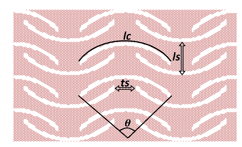
The graphene kirigami structures explored in this study were constructed by considering periodic boundary conditions such that they represent graphene films with repeating cuts Shyu et al. (2015). In order to describe our modeling strategy, in Fig.1, a sample of constructed molecular model of graphene kirigami is illustrated, along with the geometric parameters. The length of the cuts () is the first parameter that describes the graphene kirigami. The width of the cuts is accordingly changed to adjust the volume fraction of the removed materials form the graphene. In this work, we considered curved cuts which are defined by the curvature angle ( in Fig.1). This way, curvature angles of 0 and 180 degrees represent straight and half-circular cuts, respectively. The longitudinal ( in Fig.1) and transverse ( in Fig.1) spacing distances between two adjacent cuts are two other key parameters used to characterize the graphene kirigami structures. In our modeling, the cut length was considered as the main factor, which directly determines the system scale. Therefore by changing the cut length we scaled the other parameters of kirigami to keep the structural pattern comparable.
II.2 Stretchability and thermal transport properties
We employed classical molecular dynamics (MD) simulations to evaluate mechanical and thermal transport properties of graphene kirigami structures. The atomic interaction between carbon atoms was modelled using the Tersoff potential Tersoff (1988a, b) optimized by Lindsay and Broido Lindsay and Broido (2010). Among different possibilities for the modeling of graphene structures, the optimized Tersoff potential is highly efficient and can be used to simulate large scale systems. More importantly, it gives reasonable predictions of both thermal conductivity and mechanical properties of pristine graphene as compared with experimental results Xu et al. (2014); Mortazavi et al. (2016); Fan et al. (2015). In our classical MD simulations, we applied periodic boundary conditions along the x-y planar directions. The thickness of graphene kirigami nanomembranes was taken as 3.35 Å. We employed the equilibrium molecular dynamics (EMD) method to calculate the thermal conductivity of the graphene kirigami structures, using GPUMD Fan et al. (2016a), an efficient MD code fully-implemented on graphics processing units, to compute the thermal conductivity of large scale graphene kirigami structures. We calculated the heat flux vector with the appropriate form for many-body potentials as described in Fan et al. (2015):
| (1) |
where is the velocity of atom , is the position vector of atom , is the position vector from atoms to , and is the potential energy associated with atom . The thermal conductivity tensor can be acquired based on the Green-Kubo formula:
| (2) |
where is Boltzmann’s constant,
is the simulation temperature,
and is the total volume of the system.
Thermal transport in graphene kirigami nanomembranes is anisotropic,
and the thermal conductivities for a given sample
were calculated in both the longitudinal and transverse directions.
We note that when using the EMD method,
accurately predicting the converged thermal conductivity requires doing many
independent simulations and averaging them Schelling et al. (2002).
We remind that because of the use of an inaccurate heat-flux formula
for many-body interactions, the LAMMPS Plimpton (1995) implementation of the
EMD method significantly underestimates the thermal conductivity of graphene Fan et al. (2015).
Then, we evaluated the mechanical response of graphene kirigami structures by performing uniaxial tensile tests at room temperatures. In this case we used LAMMPS Plimpton (1995), a free and open-source package. As it was discussed in a recent study Mortazavi et al. (2016), we modified the inner cutoff of the Tersoff potential from 0.18 nm to 0.20 nm, which was found to accurately reproduce the experimental results for the mechanical properties of pristine graphene. The time increment of these simulations was set as 0.2 fs. Before applying the loading conditions, all structures were relaxed and equilibrated using the Nosé-Hoover barostat and thermostat method (NPT ensemble). For the loading condition, we increased the periodic size of the simulation box along the loading direction at every time step by an engineering strain rate of s-1. Simultaneously, in order to ensure the uniaxial stress condition, the stress along the transverse direction was controlled using the NPT ensemble Mortazavi et al. (2016). To report the stress-strain relations, we calculated the Virial stresses every 2 fs and then averaged them over every 20 ps intervals.
II.3 Electronic transport properties
The electronic and transport calculations, including electronic densities of states (DOS) per unit of surface () and Kubo-Greenwood conductivities (), rely on a well established real-space Kubo-Greenwood method D. Mayou and S.N. Khanna (1995); Triozon et al. (2002); Latil et al. (2004); Leconte et al. (2011); Lherbier et al. (2012); Uppstu et al. (2014). The electronic framework is based on a tight-binding (TB) Hamiltonian described by a - TB orthogonal model (one orbital per carbon atom) with interactions up to the third nearest neighbors (hopping terms are obtained as , with eV and Å ) Pereira et al. (2009); Lherbier et al. (2013). The Kubo-Greenwood approach combines a Lanczos recursion scheme to obtain the spectral quantities as the DOS Haydock (1980) and a Chebyshev polynomial expansion method to compute the time-dependent electronic diffusivity () through the evaluation of the time evolution operator , with the chosen time step. The total diffusivity is expressed as with and . Traces are evaluated by averaging on eight random phase wave packets () on large enough systems. More explicitely, for a given operator one has , where is the orbital over orbitals and is a random phase wave packet ( is a random angle). At short time, is linear in time with the slope being the average square velocity v. In the following, the considered graphene kirigami structures are constructed by repeating periodically a rectangular unit cell whose dimensions increases with the cut length ( 10, 20, 40, 80, and 160 nm). Because of this perfect periodicity, i.e. without the introduction of any stochastic disorder, the long time behavior of the diffusivity should be in the ballistic regime, i.e. a linear increase in time with the slope being v. These two ballistic regimes and its associated velocities (v and v) are in principle different. The short time velocity corresponds to the dynamics of charge at a small scale, i.e. graphene honeycomb lattice, while the long time velocity corresponds to the propagation associated to Bloch states of the periodic kirigami structure. However, to observe this second ballistic signature, the simulated time propagation has to be very long, especially for the large cuts, such that the periodicity effects at large scale become sufficiently significant. Actually, because of computing limitations this second ballistic regime is not always reached. In between these two ballistic regimes an intermediate regime should be observed and may include (pseudo) diffusive and/or localization regimes, that is a (slow increase) saturation of and/or a decrease of , respectively. These regimes correspond to the fact that at intermediate length scale, the electron wave propagation encounter scattering related to the presence of cuts and interferences related to these multiple scattering events. Similar transient phenomena was observed in a previous study on carbon nanotubes doped periodically with nitrogen atoms Khalfoun et al. (2015). The determination of mean elastic scattering times and paths ( and , respectively) is not easily practicable in systems containing two periodic patterns, which are in the present case the honeycomb and the kirigami lattices, because of the complex dynamics of charge carriers. Instead of characterizing the systems with the evaluation of and , it is preferable to describe the transport with a well-defined quantity which is the Kubo-Greenwood length-dependent conductivity (). Since the kirigami structures present anisotropy, it is also important to consider independently the two longitudinal components of the conductivity tensor ( and ). The former reads .
III Results and discussions
III.1 Thermal transport
We first study heat transport along the graphene kirigami films. Since in the EMD method periodic boundary conditions are applied and the systems are at equilibrium (no external heat-flux or temperature boundary conditions are applied), this method is much less sensitive to the finite-size effects as compared to the non-equilibrium molecular dynamics (NEMD) method Schelling et al. (2002) or the approach-to-equilibrium method (AEMD) Lampin et al. (2013). As discussed in a recent study Fan et al. (2016b), the EMD method predicts a thermal conductivity of 2900100 W/mK for pristine graphene at room temperature. In this case, a relatively small simulation cell size (with 104 atoms) is sufficient to eliminate the finite-size effects Fan et al. (2015). However, using the NEMD or the AEMD method, the thermal conductivity of graphene keeps increasing by increasing the sheet length and the thermal conductivity was found to not fully converge even up to 0.1 mm Barbarino et al. (2015). Interestingly, for the graphene kirigami structures with periodic cutting patterns, the EMD method can be used to evaluate the full thermal conductivity tensor by constructing a single sample of moderate size. Whereas using the NEMD or AEMD method the length dependency of the predicted thermal conductivity values should be assessed, which demands high computational costs associated with the modeling of several large samples, each with different lengths.
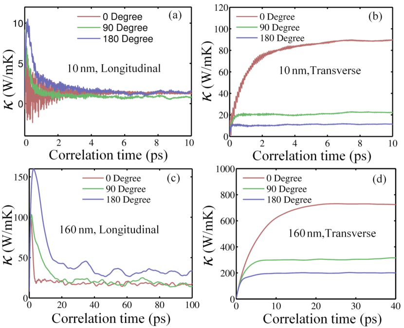
In Fig.2, typical EMD results for the calculated thermal conductivity
along the longitudinal and transverse directions are presented as a function of correlation time,
for graphene kirigami samples with cut lengths of 10 nm and 160 nm
at room temperature. In this case, the volume fraction of the cuts is 20%
and samples with curvature angles of
0∘, 90∘ and 180∘ for the cuts are considered.
For samples with larger cut length,
the predicted thermal conductivity values are considerably higher (see Fig.2).
As expected, along the longitudinal direction, since
the cut sections interfere directly with the phonon transport,
the thermal conductivity is much more suppressed as compared with the
transverse direction in which the cuts are basically parallel
to the heat transfer direction.
Moreover, based on our results along the longitudinal direction
for sample with small cut lengths, the effects of cuts curvature angle
on the thermal conductivity are small.
The running thermal conductivity in this direction also exhibits
a local peak at small correlation time,
which is a sign of pseudo diffusive transport and localization
caused by the combined honeycomb and kirigami lattices,
as in the case of electron transport (see the method section).
For the heat transfer along the transverse direction,
by increasing the curvature angle the thermal conductivity
decreases significantly,
which can be related to the increased obstruction
in the direction of the phonon transport.
In a recent investigation Fan et al. (2016b), a decomposition of the thermal conductivity of 2D materials into contributions from in-plane and out-of-plane phonons was introduced. For pristine graphene the out-of-plane and in-plane components of the thermal conductivity were predicted to be 2050 W/mK and 850 W/mK, respectively.
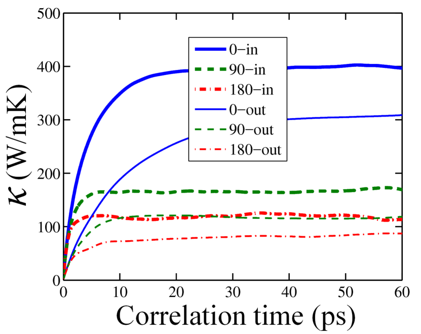
To gain more insight concerning the underlying mechanisms responsible for
the suppression of thermal conductivity along the graphene kirigami structures,
the calculated out-of-plane and in-plane thermal conductivity components
are compared in Fig.3 along the transverse direction
for graphene kirigami networks with 20% concentration of 160 nm long cuts.
In contrast to the thermal transport
in the pristine graphene, the in-plane phonons contribute more to the thermal conductivity
than the out-of-plane phonons in graphene kirigami structures.
For example, in the case of 0 degree cuts,
the in-plane and out-of-plane thermal conductivity components
are about 400 W/mK and 300 W/mK, respectively,
which are about 1/2 and 1/7 of the corresponding values in pristine graphene.
This clearly demonstrates that the suppression of out-of-plane phonons plays
the major role in the decline of the thermal transport along graphene kirigami films.
For the kirigami systems at atomic scale, the thermal transport is complicated since the phonons-cut scattering effects play the major role in the heat transport. However, by increasing the system size and approaching the mean-free-path of graphene the effect of phonon-cut scattering decreases. Consequently, for the kirigami structures with the large cuts in microscale the effective thermal conductivity approaches the diffusive heat transfer which can be studied on the basis of a continuum system that neglects the phonon scattering rates. Nonetheless, from continuum point of view, the effective thermal conductivity along kirigami structures is not trivial and to the best of our knowledge no analytical function exists to describe such a diffusive process. We therefore employed finite element (FE) modeling to evaluate the effective thermal conductivity of kirigami films at the diffusive limit. In this study, the FE simulations were carried out using the ABAQUS/Standard package. As for the loading condition, we applied positive (inward) and negative (outward) heat-fluxes on the two opposite surfaces along the direction in order to investigate the thermal conductivity. Since the thermal transport is investigated along periodic structures, on the boundary edges perpendicular of the heat-transfer direction the temperatures of every two opposite nodes should be equal which can be achieved by applying periodic boundary condition in the FE modeling. We calculated the temperature gradient along the heat transfer direction which was then accordingly used to compute the effective thermal conductivity on the basis of Fourier’s law Mortazavi et al. (2014). To count for atomistic effects which are related to the phonon-cut scattering rates, one can assume these cuts as resistors that scatter the phonons. In such a way, the effective thermal conductivity of kirigami films can be approximated by considering a series of line conductors (representing the graphene pristine lattices) that are connected by thermal resistors (representing the cuts). As discussed in an earlier study for the modeling of heat transfer in polycrystalline graphene Mortazavi et al. (2014), the effective thermal conductivity of such a system can be represented based on the first order rational curve. In order to simulate the effective thermal conductivity of graphene kirigami structures with larger cut lengths, we therefore extrapolated the EMD results for small cut lengths using the first order rational curve. In these cases, we considered that the thermal conductivity for the kirigami films with infinite cut lengths is equal to that based on our FE diffusive modeling.
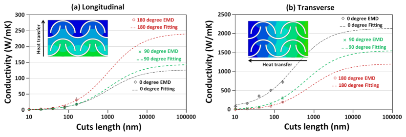
In Fig.4, the calculated effective thermal conductivities of graphene kirigami structures by the EMD method as a function of cuts length along the longitudinal and transverse directions are illustrated. Interestingly, the devised extrapolation technique can fairly well reproduce the trends acquired by the fully atomistic EMD modeling. This result suggests that combination of EMD and FE modeling can be used as an efficient approach to estimate and engineer the effective thermal conductivity of graphene kirigami structures for different cut lengths and curvature angles as well. We should also note that the thermal conductivity of graphene can be engineered by at least three orders of magnitude based on the kirigami approach. We remind that the thermal conductivity of highly defective graphene so called amorphized graphene was found to be around two orders of magnitude smaller than that of pristine graphene Mortazavi et al. (2016). Moreover, chemical doping was predicted to decline the thermal conductivity of graphene by around an order of magnitude Mortazavi and Ahzi (2012). This short comparison clearly highlights that the fabrication of graphene kirigami networks can be considered as a very effective method to tune the thermal transport properties in graphene-based nanostructures.
III.2 Stretchability
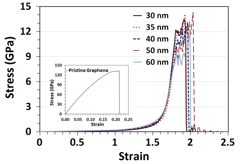
We next shift our attention to explore the mechanical response and stretchability of the graphene kirigami structures. As observed for thermal transport, due to the phonon-cut scattering effects the cut length plays the major role. In contrast, for the stretchability of the graphene kirigami, the deflection of the sheets and stress-concentration originated from the cuts are the main factor that should be taken into account. To investigate the effect of cut length on the stress-strain response, we considered different structures with linear cuts and with different cut lengths and the acquired results are illustrated in Fig.5. As compared with pristine graphene (Fig.5 inset), the stress-strain responses of graphene kirigami present different patterns. In pristine graphene, the applied strain directly results in increasing of the carbon atoms bond length and therefore the stress value increases considerably by increasing the strain. On the contrary for the considered graphene kirigami structures, up to high strain levels of 1, the stress value only slightly increases and remains very low which indicates that the structure elongates by deflection rather than the stretching of the carbon bonds. After the strain level of 1, the stress values start to increase but smoothly which implies that the deformation is yet achieved by the deflection but bond elongation is also happening. For the considered structures, at strain levels higher than 1.6 the stress values sharply increase which reveals that the deflection of the sheets contribute less and the stretching is achieved more by the bond elongation. Because of the limited stretchability of the carbon atoms bond, this step is limited and shortly after the structure reaches its failure point. At this stage, the stress concentration existing around the cut corners result in the local and instantaneous bond breakages thus causing instabilities and accordingly variations in the stress values. Around the cut corners, the bond breakages extend gradually and the rapture finally occurs when the two parts of the kirigami become completely detached by the crack coalescence. Since we considered the thermal effects by conducting the simulation at room temperature, the bond breakages present stochastic nature and therefore a sample present different stress-strain relations around the failure point by performing independent simulations with different initial velocities. In accordance with earlier observations Qi et al. (2014), our results depicted in Fig.5 also confirm that the stretchability of the graphene kirigami is convincingly independent of the cut length. This in an important finding and illustrates that the classical MD simulations can be considered as a promising approach for the design of graphene kirigami structures with optimized performance. Worthy to note that in this case, the finite element modeling are highly complicated mainly because of the existing severe out-of plane deflections and also stress-concentrations (that may cause singularity in the stress field). As it is clear for different samples, the variations for the maximum tensile strength is more considerable than the rupture strain of the graphene kirigami films. From an engineering point of view, the main goal to fabricate the graphene kirigami is to enhance the stretchability such that the values for the tensile strength are not critical. For the rest of our investigation, we considered the cut length of 40 nm and for each case we performed 4 independent simulations to provide the error-bars in our results.
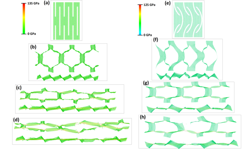
In Fig.6, the deformation process of two different graphene kirigami structures are depicted. The deformation is highly symmetrical which verifies the accuracy of our applied loading condition and also confirms that the our modeling results are representative of graphene kirigami structures with periodic pattern of cuts. Moreover, up to high strain levels the stretching is achieved by the sheets out-of plane deflections and transverse shrinkage and the stress values throughout the sample are negligible, though in the cuts corner due to stress concentration they may instantaneously reach high values (Fig.6(b) and Fig.6(f)). At higher strain levels around the failure, stress concentration increases around the cuts corner which initiate the spontaneous bond breakage (Fig.6(b) and Fig.6(f)), finally leading to the sample rupture (Fig.6(d) and Fig.6(h)). As it is clear, to design highly stretchable graphene kirigami, the solution is to enhance the deflection limit of the structures. In this regard, linear cuts are more favorable since they can deflect more than curved cuts. In addition, simple comparison based on Fig.6 results reveals that upon the stretching, the kirigami structure with linear cuts shrink more along the transverse direction in comparison with the curved cuts. To provide a general viewpoint concerning the engineering of the graphene kirigami mechanical response, we studied the effects of various design parameters. To this aim, we compared the rupture strain and tensile strength for different kirigami structures. The rupture strain is the key parameter which is representative of the stretchability of the graphene nanomembranes. The stress field in linear elastic fracture mechanics (LEFM) in a two dimensional solid for a straight crack can be described in terms of the mode I and II stress intensity factors. We should however emphasis that although our study is categorized as a large deformation problem, but the insight provided by the LEFM for small strain theory can be helpful to understand the underlying mechanism. The stress intensity factor for the arrangement of cracks in transverse direction can be computed using the standard fracture mechanics techniques, as follows:
| (3) |
Here is the cut length and is the sum of cut length and transverse spacing distance.
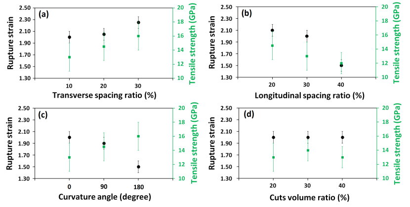
As illustrated in Fig.7(a), by increasing the transverse spacing ratio, both the rupture strain and the tensile strength increase. The increase in the maximum tensile strength is more considerable than the increase in the stretchability. The value of the stress near the cut tip decreases with increasing the transverse distance. Therefore, the larger the transverse spacing between the cracks, the less is the influence from the interaction of the near tip stress fields. According to Eq. 3, the stress-intensity factor decreases by increasing the transverse spacing distance due to suppression of the interaction of the stress fields of adjacent cuts. Consequently, by increasing the transverse spacing ratio the stress-concentration decreases and such that the tensile strength increases. Note that for a very high transverse spacing the graphene kirigami approaches to the graphene structure with few cracks inside, which yields to a failure strain lower than that of the pristine graphene. For the graphene kirigami accordingly there should be an optimum transverse spacing distance that maximizes the stretchability. The situation is opposite for the increase of longitudinal spacing ratio. Indeed, by increasing the longitudinal spacing the stretchability drops significantly. This is an expected trend because the stretchability of the kirigami structures is basically originated from the longitudinal spacing. By increasing the longitudinal spacing, the out-of-plane deflection decreases and the structure approaches to the graphene film with cracks. Regarding the cuts curvature angle, we found that the linear cuts present the highest stretchability as illustrated in Fig.7(c). For the linear cuts, the rupture strain is higher than the one for curved cracks due to the fact that the effective distance between two curved cuts becomes much smaller. Hence, for the curved cuts the film deflection decreases and additionally the crack path until coalescence is shorter and therefore the stretchability is not as high as for the linear cuts. Nonetheless, it has been shown by Karihaloo Karihaloo (1982), that the stress intensity factor for a curved crack compared to that of the straight crack of same length being positioned at the same location and subjected to far field stress is lower. Therefore by increasing the cuts curvature angle, the stress concentration decreases and such that the tensile strength increases. Interestingly, for the cuts volume fraction we found that it does not yield considerable effects neither on the stretchability nor on the tensile strength (see Fig.7(d)). Based on our brief parametric investigation, the transverse and longitudinal spacing ratios can be considered as the two main factors that could be optimized to increase both, stretchability and tensile strength. Our results also clearly confirm that the graphene kirigami structures can be stretchable by more than 10 times as compared with the pristine graphene.
III.3 Electronic structures
After having explored their thermal and mechanical properties, we now focus on the electronic structure properties of the graphene kirigami. First, the density of states (DOS) of various graphene kirigami structures are presented in Fig.8. The total widths/lengths of the large systems vary between 320 and 390 nm and are obtained by repeating the unit cells as illustrated in Figs.8(left panels). The total size of the system is large enough to ensure an accurate energy resolution within the Lanczos technique and also a rapid convergence of the average on random phase wave packets. Note that three different angles were considered for the cuts, =0, 90, and 180∘. For =0∘, the cuts are actually straight (Fig.8(a-d)), while for 90 and 180∘, the cuts are curved (Fig.8(f-i,k-n)). For each , five different cut lengths are considered, =10, 20, 40, 80, and 160 nm (the unit cells of the =160 nm systems are not shown in Fig.8).
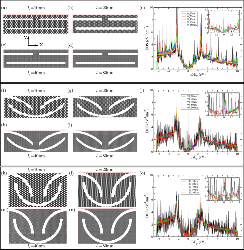
The DOS of the case =0∘, for different cut lengths are presented in Fig.8(e), while the DOS corresponding to =90 and 180∘ are depicted in Fig.8(j) and Fig.8(o), respectively. One recognizes easily the global shape of the graphene DOS corresponding to the and bands, i.e. a Heaviside function at the band edges ( point in graphene Brillouin zone (BZ)), two van Hove singularities ( point in the BZ), and a V-shape, i.e. a linear increase as a function of energy around the Dirac point ( point in the BZ). However, one also obviously notices the presence of many DOS sub-peaks which can be attributed to van Hove singularities typical of 1D systems, which appear because of the formation of connected nanoribbons generated by the cuts in graphene. The energy spacing between these 1D van Hove singularities is inversely proportional to the ribbon’s width. For very thin ribbons (10 nm cases, see for instance Fig.8(a)), the DOS is quite spiky and deviates considerably from the pristine graphene DOS, in particular close to the Fermi energy (Dirac point in graphene) where the DOS sub-structure is complex (see insets in Fig.8(e,j,o)). In particular, small energy gaps can appear as observed for instance for (90∘,10 nm) and (180∘,10 nm) while a more significant gap is observed for (0∘,20 nm) in the energy range [-0.2,+0.2] eV with a peak centered on the zero energy. However, when increasing the DOS recovers progressively the shape of pristine graphene DOS although residual oscillations coming from the 1D van Hove singularities are still present. Note that for =90 and 180∘, although the DOS become similar to graphene DOS, a non-negligible peak remains present around the Fermi energy (see for instance =80, 160 nm curves in the insets of Fig.8(j,o)). Those persistent peaks are originating from strongly localized states, most probably located close to the cut edges, similarly to what was observed for vacancies in graphene Cresti et al. (2013). Such localized states can affect the electronic transport and can possibly induce a transport gap in the corresponding energy window.
III.4 Electronic transport
Recently, Bahamon et al. discussed the electronic transport in 34 nm long and 10 nm wide 1D graphene kirigami structures with straight cuts using the Landauer-Büttiker formalism Bahamon et al. (2016). They observed that at this nanoscale size the 1D electronic transport is governed by resonant tunneling through coupled localized states acting as quantum dots. Upon moderate elongation (15%), the conductance profile is first degraded because of the decoupling of the states but it can revive at a larger elongation (30%).
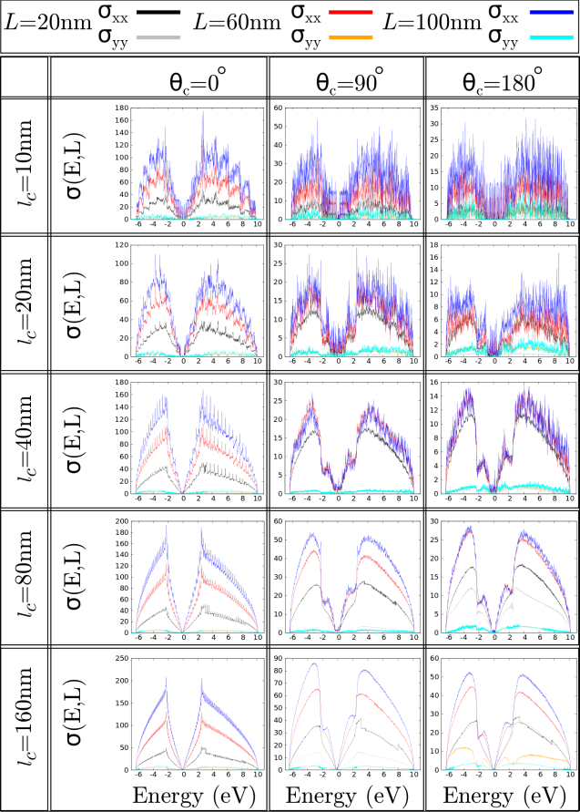
Here, the electronic transport properties of unstretched 2D periodic graphene kirigami are investigated using the real-space Kubo-Greenwood method. As discussed in the method section, the Kubo-Greenwood formalism allow us to describe the electronic diffusion and the associated conductivity. The diffusivity curves are presented in the supplementary information document. They illustrate the discussion conducted in the method section regarding the presence of the two-scale periodicity and its impact on the ballistic and intermediate diffusive/localized transport regimes. However, in order to gain more insight and obtain a more concrete picture of the electronic transport properties in these systems it is preferable to characterize them through the energy- and length-dependent Kubo-Greenwood conductivity . The longitudinal components of the conductivity tensor and have been calculated for three specific propagation length 20, 60 and 100 nm and are presented in Fig.9. One can immediately notice three points. First, it is clear that the conductivities along the Y direction (gray, orange and cyan curves) are much lower than the conductivities along the X direction (black, red and blue curves). Second, the increase of the cut angle from =0∘ to =180∘ (i.e. from left to right panels) decreases the overall conductivity profile in absolute values. Finally, the transition from a 1D nanoribbon-like to a 2D graphene-like electronic transport is clearly visible when going from small to large cut lengths (i.e. from top to bottom panels) as the 1D subbands structure is progressively smoothened out. The conductivities and are found to globally increase with propagation length although the increase is not really significant for which is maintained to low values. Actually for high cut angle and long cut lengths, displays a decreasing behavior synonym of localization effects. Note also that for the propagation length 100 nm is not reached at all energies because of the slow propagation velocities in this direction. As for thermal transport, these results demonstrate a strong anisotropy between the two principal electronic transport directions. Then, as noticed in the DOS, the presence of a band gap is clearly observed in the system =(0∘,20 nm). Interestingly, the general shape of for curved cuts is different from the =0∘ case. Indeed, the electron/hole regions (positive/negative charge carrier energies) exhibit two main peaks instead of only one. There is no particular features in the DOS that would help to explain this double peak structure. Actually, it is interesting to note that for =(180∘,160 nm) the conductivity curve exhibit a single peak structure at small propagation length (20 nm) before showing a double peak structure at longer propagation length (100 nm). Overall, a conductivity ratio 10–20 can be estimated.
IV Concluding remarks
Extensive atomistic simulations were conducted to explore the electronic and thermal transport as well as the stretchability of graphene kirigami structures. The properties of graphene kirigami structures were investigated using periodic patterns of linear and curved cuts. Equilibrium molecular dynamics (EMD) method was used to calculate the effective thermal conductivity of graphene kirigami structures at atomic scale. The thermal transport is found to be highly anisotropic and the phonons-cut scattering effect plays the major role in the heat transport. The effective thermal conductivity of graphene kirigami structures as a function of cut lengths was established by extrapolating the EMD results for small cut lengths to the estimation based on the finite element (FE) diffusive modeling. It was confirmed that the proposed combination of EMD and FE modeling can be accurately used to evaluate the effective thermal conductivity of graphene kirigami structures from nano to macro scale. Notably, our results suggest that the thermal conductivity of graphene can be engineered by more than three orders of magnitude based on the kirigami approach. Then the mechanical response of graphene kirigami structures were investigated by performing uniaxial tensile molecular dynamics simulations. Up to high strain levels, the kirigami structure elongates by out-of-plane deflection rather than bond stretching and thus the stress values remain negligible. The stress values later start to increase smoothly implying that bond elongation also occurs. Before the failure point, the stress values increase sharply and the existing stress concentrations around the cuts corner result in bond breakages and finally leads to the sample rupture. Consequently, the stretchability of the graphene kirigami was suggested to directly correlate to the out-of-plane deflection limit of the structure which can be improved by using the straight cuts with optimized transverse and longitudinal spacing ratios. Finally, electronic transport was investigated. The electronic density of states displayed series of van Hove peaks which are signature of one-dimensional confinement in case of graphene kirigami at the nanoscale. Band gaps can even occur in some cases, as well as transport gaps caused by strongly localized states especially in curved cuts. Finally, electronic conductivities are found to be highly anisotropic with a ratio of 10–20. Unfortunately, this electronic anisotropy is analogous to the thermal anisotropy which is in principle not in favor of thermoelectric applications. However, as discussed, the tunability of graphene kirigami properties is very large and therefore may open routes towards thermoelectric engeenering and new kinds of ultra thin NEMS with superior properties.
V Acknowledgements
B.M. and T.R. greatly acknowledge the financial support by European Research Council for COMBAT project (Grant number 615132). Z.F. and A.H. are supported by the National Natural Science Foundation of China (Grant No. 11404033) and the Academy of Finland through its Centres of Excellence Program (project no. 251748) and they acknowledge the computational resources provided by Aalto Science-IT project and Finland’s IT Center for Science (CSC). A.L., and J.-C.C. acknowledge financial support from the Fédération Wallonie-Bruxelles through the ARC entitled 3D Nanoarchitecturing of 2D crystals (No 16/21-077), from the European Union’s Horizon 2020 research and innovation programme (No 696656), and from the Belgium FNRS. Computational resources have been partly provided by the supercomputing facilities of the Université catholique de Louvain (CISM/UCL) and the Consortium des Équipements de Calcul Intensif en Fédération Wallonie Bruxelles (CÉCI) funded by the Fond de la Recherche Scientifique de Belgique (F.R.S.-FNRS) under convention 2.5020.11
References
- Novoselov et al. (2004) K. S. Novoselov, A. K. Geim, S. V. Morozov, D. Jiang, Y. Zhang, S. V. Dubonos, I. V. Grigorieva, and A. A. Firsov, Science 306, 666 (2004).
- Geim and Novoselov (2007) A. K. Geim and K. S. Novoselov, Nat Mater 6, 183 (2007).
- Castro Neto et al. (2009) A. H. Castro Neto, F. Guinea, N. M. R. Peres, K. S. Novoselov, and A. K. Geim, Rev. Mod. Phys. 81, 109 (2009).
- Lee et al. (2008) C. Lee, X. Wei, J. W. Kysar, and J. Hone, Science 321, 385 (2008).
- Balandin (2011) A. A. Balandin, Nat Mater 10, 569 (2011).
- Ghosh et al. (2010) S. Ghosh, W. Bao, D. L. Nika, S. Subrina, E. P. Pokatilov, C. N. Lau, and A. A. Balandin, Nat Mater 9, 555 (2010).
- Kubota et al. (2007) Y. Kubota, K. Watanabe, O. Tsuda, and T. Taniguchi, Science 317, 932 (2007).
- Aufray et al. (2010) B. Aufray, A. Kara, S. Vizzini, H. Oughaddou, C. Léandri, B. Ealet, and G. L. Lay, Applied Physics Letters 96, 183102 (2010).
- Vogt et al. (2012) P. Vogt, P. De Padova, C. Quaresima, J. Avila, E. Frantzeskakis, M. C. Asensio, A. Resta, B. Ealet, and G. Le Lay, Phys. Rev. Lett. 108, 155501 (2012).
- Das et al. (2014) S. Das, M. Demarteau, and A. Roelofs, ACS Nano 8, 11730 (2014).
- Li et al. (2014) L. Li, Y. Yu, G. J. Ye, Q. Ge, X. Ou, H. Wu, D. Feng, X. H. Chen, and Y. Zhang, Nat Nano 9, 372 (2014).
- Mannix et al. (2015) A. J. Mannix, X.-F. Zhou, B. Kiraly, J. D. Wood, D. Alducin, B. D. Myers, X. Liu, B. L. Fisher, U. Santiago, J. R. Guest, M. J. Yacaman, A. Ponce, A. R. Oganov, M. C. Hersam, and N. P. Guisinger, Science 350, 1513 (2015).
- Bianco et al. (2013) E. Bianco, S. Butler, S. Jiang, O. D. Restrepo, W. Windl, and J. E. Goldberger, ACS Nano 7, 4414 (2013).
- Radisavljevic et al. (2011) B. Radisavljevic, A. Radenovic, J. Brivio, V. Giacometti, and A. Kis, Nat Nano 6, 147 (2011).
- Guinea (2012) F. Guinea, Solid State Communications 152, 1437 (2012).
- Metzger et al. (2010) C. Metzger, S. Rémi, M. Liu, S. V. Kusminskiy, A. H. Castro Neto, A. K. Swan, and B. B. Goldberg, Nano Letters 10, 6 (2010).
- Pereira and Castro Neto (2009) V. M. Pereira and A. H. Castro Neto, Phys. Rev. Lett. 103, 046801 (2009).
- Barraza-Lopez et al. (2013) S. Barraza-Lopez, A. A. P. Sanjuan, Z. Wang, and M. Vanević, Solid State Communications 166, 70 (2013).
- Guinea et al. (2010) F. Guinea, M. I. Katsnelson, and A. K. Geim, Nat Phys 6, 30 (2010).
- Banhart et al. (2011) F. Banhart, J. Kotakoski, and A. V. Krasheninnikov, ACS Nano 5, 26 (2011).
- Lherbier et al. (2012) A. Lherbier, S. M.-M. Dubois, X. Declerck, Y.-M. Niquet, S. Roche, and J.-C. Charlier, Phys. Rev. B 86, 075402 (2012).
- Cummings et al. (2014) A. W. Cummings, D. L. Duong, V. L. Nguyen, D. Van Tuan, J. Kotakoski, J. E. Barrios Vargas, Y. H. Lee, and S. Roche, Advanced Materials 26, 5079 (2014).
- Cresti et al. (2008) A. Cresti, N. Nemec, B. Biel, G. Niebler, F. Triozon, G. Cuniberti, and S. Roche, Nano Research 1, 361 (2008).
- Wehling et al. (2008) T. O. Wehling, K. S. Novoselov, S. V. Morozov, E. E. Vdovin, M. I. Katsnelson, A. K. Geim, and A. I. Lichtenstein, Nano Letters 8, 173 (2008).
- Lherbier et al. (2008) A. Lherbier, X. Blase, Y.-M. Niquet, F. m. c. Triozon, and S. Roche, Phys. Rev. Lett. 101, 036808 (2008).
- Wang et al. (2008) X. Wang, L. Zhi, and K. Müllen, Nano Letters 8, 323 (2008).
- Schedin et al. (2007) F. Schedin, A. K. Geim, S. V. Morozov, E. W. Hill, P. Blake, M. I. Katsnelson, and K. S. Novoselov, Nat Mater 6, 652 (2007).
- Miao et al. (2012) X. Miao, S. Tongay, M. K. Petterson, K. Berke, A. G. Rinzler, B. R. Appleton, and A. F. Hebard, Nano Letters 12, 2745 (2012).
- Soriano et al. (2015) D. Soriano, D. V. Tuan, S. M.-M. Dubois, M. Gmitra, A. W. Cummings, D. Kochan, F. Ortmann, J.-C. Charlier, J. Fabian, and S. Roche, 2D Materials 2, 022002 (2015).
- Zhang et al. (2014) P. Zhang, L. Ma, F. Fan, Z. Zeng, C. Peng, P. E. Loya, Z. Liu, Y. Gong, J. Zhang, X. Zhang, P. M. Ajayan, T. Zhu, and J. Lou, Nature Communications 5, 3782 (2014).
- Blees et al. (2015) M. K. Blees, A. W. Barnard, P. A. Rose, S. P. Roberts, K. L. McGill, P. Y. Huang, A. R. Ruyack, J. W. Kevek, B. Kobrin, D. A. Muller, and P. L. McEuen, Nature 524, 204 (2015).
- Qi et al. (2014) Z. Qi, D. K. Campbell, and H. S. Park, Phys. Rev. B 90, 245437 (2014).
- Wei et al. (2016) N. Wei, Y. Chen, K. Cai, J. Zhao, H.-Q. Wang, and J.-C. Zheng, Carbon 104, 203 (2016).
- Shyu et al. (2015) T. C. Shyu, P. F. Damasceno, P. M. Dodd, A. Lamoureux, L. Xu, M. Shlian, M. Shtein, S. C. Glotzer, and N. A. Kotov, Nat Mater 14, 785 (2015).
- Tersoff (1988a) J. Tersoff, Phys. Rev. B 37, 6991 (1988a).
- Tersoff (1988b) J. Tersoff, Phys. Rev. Lett. 61, 2879 (1988b).
- Lindsay and Broido (2010) L. Lindsay and D. A. Broido, Phys. Rev. B 81, 205441 (2010).
- Xu et al. (2014) X. Xu, L. F. C. Pereira, Y. Wang, J. Wu, K. Zhang, X. Zhao, S. Bae, C. Tinh Bui, R. Xie, J. T. L. Thong, B. H. Hong, K. P. Loh, D. Donadio, B. Li, and B. Özyilmaz, Nature Communications 5, 3689 (2014).
- Mortazavi et al. (2016) B. Mortazavi, Z. Fan, L. F. C. Pereira, A. Harju, and T. Rabczuk, Carbon 103, 318 (2016).
- Fan et al. (2015) Z. Fan, L. F. C. Pereira, H.-Q. Wang, J.-C. Zheng, D. Donadio, and A. Harju, Phys. Rev. B 92, 094301 (2015).
- Fan et al. (2016a) Z. Fan, W. Chen, V. Vierimaa, and A. Harju, arXiv:1610.03343 [physics.comp-ph] (2016a).
- Schelling et al. (2002) P. K. Schelling, S. R. Phillpot, and P. Keblinski, Phys. Rev. B 65, 144306 (2002).
- Plimpton (1995) S. Plimpton, Journal of Computational Physics 117, 1 (1995).
- D. Mayou and S.N. Khanna (1995) D. Mayou and S.N. Khanna, J. Phys. I France 5, 1199 (1995).
- Triozon et al. (2002) F. Triozon, J. Vidal, R. Mosseri, and D. Mayou, Phys. Rev. B 65, 220202 (2002).
- Latil et al. (2004) S. Latil, S. Roche, D. Mayou, and J.-C. Charlier, Phys. Rev. Lett. 92, 256805 (2004).
- Leconte et al. (2011) N. Leconte, A. Lherbier, F. Varchon, P. Ordejón, S. Roche, and J.-C. Charlier, Phys. Rev. B 84, 235420 (2011).
- Uppstu et al. (2014) A. Uppstu, Z. Fan, and A. Harju, Phys. Rev. B 89, 075420 (2014).
- Pereira et al. (2009) V. M. Pereira, A. H. Castro Neto, and N. M. R. Peres, Phys. Rev. B 80, 045401 (2009).
- Lherbier et al. (2013) A. Lherbier, S. Roche, O. A. Restrepo, Y.-M. Niquet, A. Delcorte, and J.-C. Charlier, Nano Research 6, 326 (2013).
- Haydock (1980) R. Haydock, Computer Physics Communications 20, 11 (1980).
- Khalfoun et al. (2015) H. Khalfoun, A. Lherbier, P. Lambin, L. Henrard, and J.-C. Charlier, Phys. Rev. B 91, 035428 (2015).
- Lampin et al. (2013) E. Lampin, P. L. Palla, P.-A. Francioso, and F. Cleri, Journal of Applied Physics 114, 033525 (2013).
- Fan et al. (2016b) Z. Fan, L. F. C. Pereira, P. Hirvonen, M. M. Ervasti, K. R. Elder, D. Donadio, T. Ala-Nissila, and A. Harju, arXiv:1612.07199 [cond-mat.mes-hall] (2016b).
- Barbarino et al. (2015) G. Barbarino, C. Melis, and L. Colombo, Phys. Rev. B 91, 035416 (2015).
- Mortazavi et al. (2014) B. Mortazavi, M. Potschke, and G. Cuniberti, Nanoscale 6, 3344 (2014).
- Mortazavi and Ahzi (2012) B. Mortazavi and S. Ahzi, Solid State Communications 152, 1503 (2012).
- Stukowski (2010) A. Stukowski, Modelling and Simulation in Materials Science and Engineering 18, 015012 (2010).
- Karihaloo (1982) B. Karihaloo, Mechanics of Materials 1, 189 (1982).
- Cresti et al. (2013) A. Cresti, T. Louvet, F. Ortmann, D. Van Tuan, P. Lenarczyk, G. Huhs, and S. Roche, Crystals 3, 289 (2013).
- Bahamon et al. (2016) D. A. Bahamon, Z. Qi, H. S. Park, V. M. Pereira, and D. K. Campbell, Phys. Rev. B 93, 235408 (2016).
VI Supplementary information
VI.1 Electronic diffusivity
In order to display the complex dynamics of charge carriers taking place in the kirigami structures one discusses here the directional, energy and time dependent diffusivities. The diffusivities along the x direction () and along the y direction () are presented in Fig.10 for five selected energies -0.4, -0.2, 0.0, +0.2, and +0.4 eV with respect to the Fermi energy (). The top panels of Fig.10 correspond to =0∘, the middle panels to =90∘, and the bottom panels to =180∘. First, one notices that is systematically lower than by one or two orders of magnitude, indicating a clear anisotropy in the two transport directions. Second, the magnitude of the diffusivity is dependent on the energy which can be understood from the complex DOS containing numerous van Hove singularities and possible band gaps as observed in main text in Fig.8. Some diffusivity curves exhibit significant undulations which can introduced by the numerical derivatives of wave packet quadratic spreading (, ), in particular for long cut lengths 80 and 160 nm. In some cases, it even induces a negative value of the diffusivity because in the localization regime the saturating quadratic spreading is no more increasing monotonically and may slightly oscillate, i.e. has a small negative slope. This is a possible artifact of the calculation.
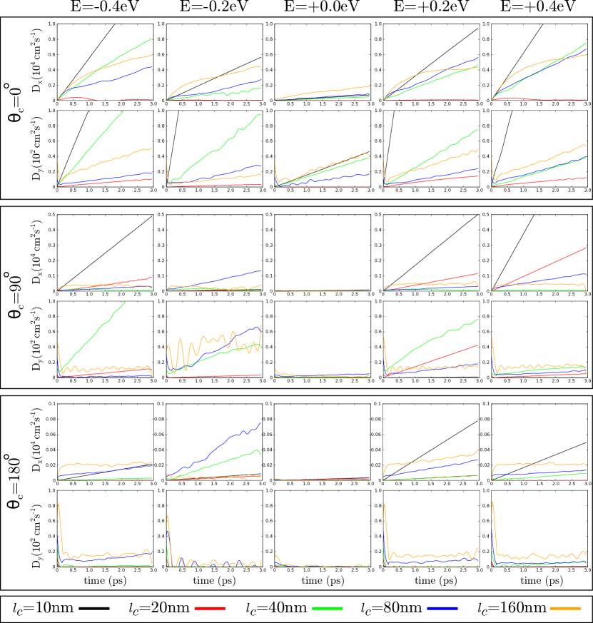
One also observes that the long time ballistic regime
discussed in the main text in section II
is easily observed for 10 nm (red curves)
but is not clearly obtained for the other systems.
For =(0∘,20 nm), the diffusivities
are found to be anomalously low compared to other systems.
However, this can be rationalized by the fact that a rather large band gap
with localized states were observed in the vicinity of the Fermi level
for this =(0∘,20 nm) graphene kirigami.
Some diffusivity curves display a diffusive regime i.e. a constant value of
(see for instance and of the
=(180∘,160 nm) for =-0.4, +0.2 and +0.4 eV),
which results from the scattering at the cut edges.
In other cases, a localized regime is observed i.e. a zero value of
corresponding to constructive quantum interferences in scattering loops
inducing localization of the wave packet.
However, as mentioned in main text in section II, at
longer propagation time the diffusivity
should finally recover a ballistic behavior
because of the periodicity.
Overall, Fig.10 demonstrates the complex transient regimes
that can be obtained in these graphene kirigami structures.