Spin circuit representation of spin pumping
Abstract
Circuit theory has been tremendously successful in translating physical equations into circuit elements in organized form for further analysis and proposing creative designs for applications. With the advent of new materials and phenomena in the field of spintronics and nanomagnetics, it is imperative to construct the spin circuit representations for different materials and phenomena. Spin pumping is a phenomenon by which a pure spin current can be injected into the adjacent layers. If the adjacent layer is a material with a high spin orbit coupling, a considerable amount of charge voltage can be generated via inverse spin Hall effect, allowing spin detection. Here we develop the spin circuit representation of spin pumping. We then combine it with the spin circuit representation for the materials having spin Hall effect to show that it reproduces the standard results in literature. We further show how complex multilayers can be analyzed by simply writing a netlist.
Spin pumping Silsbee et al. (1979); Mizukami et al. (2001a); *RefWorks:1306; *RefWorks:1304; *RefWorks:1307; *RefWorks:1308; *RefWorks:1309; *RefWorks:1310; Tserkovnyak et al. (2002a); *RefWorks:1041; Tserkovnyak et al. (2005); Costache et al. (2006); Ando et al. (2011), unlike charge pumping Brouwer (1998); *RefWorks:1324, injects a pure spin current into surrounding conductors. If the adjacent material possesses high spin-orbit coupling Kimura et al. (2007); Ando et al. (2008); Mosendz et al. (2010a); *RefWorks:813; Liu et al. (2011); *RefWorks:608; *RefWorks:758; *RefWorks:1341; *RefWorks:755; *RefWorks:1342; *RefWorks:1343), a considerable amount of charge voltage can be generated allowing the detection of spin current via inverse spin Hall effect (ISHE) Wang et al. (2006); Jiao and Bauer (2013); Azevedo et al. (2005); Saitoh et al. (2006). According to Onsager’s reciprocity Onsager (1931a); *RefWorks:1293; Jacquod et al. (2012), spin pumping and ISHE are the reciprocal phenomena Brataas et al. (2012) of spin momentum transfer Slonczewski (1996); *RefWorks:155; *RefWorks:7; *RefWorks:196 and direct spin Hall effect (SHE) Dyakonov and Perel (1971); *RefWorks:764; *RefWorks:1198; Murakami et al. (2003); *RefWorks:765; *RefWorks:902; Valenzuela and Tinkham (2006); Roy (2014), respectively and it gives us an alternative methodology to understand and estimate the relevant parameters in the system.
Kirchoff’s circuit laws (current and voltage laws, referred as KCL and KVL, respectively) have been ubiquitous in the development of the modern transistor-based technology and there are commercial programs for SPICE (Simulation Program with Integrated Circuit Emphasis), e.g., HSPICE hsp . In this way, an equivalent circuit is constructed based on the underlying physical governing equations for simplified understandings and the development of the complex designs Rabaey et al. (2003). For spintronic circuits, the voltages and currents at different nodes are of 4-components (1 for charge and 3 for spin vector) and the conductances are matrices ( basis). Such representations have been developed earlier e.g., for ferromagnet (FM), normal metal (NM), FM-NM interface, spin Hall effect (SHE) Brataas et al. (2006); Srinivasan et al. (2014); Hong et al. (2016).
Here, we construct the spin circuit representation of spin pumping. We deduce the 3-component version since spin pumping injects pure spin current (without any charge component) and show that it can reproduce the established expressions in literature for effective spin mixing conductance considering diffusive NM Tserkovnyak et al. (2005) and the inverse spin Hall voltage due to spin pumping Mosendz et al. (2010a); *RefWorks:813. We further employ such spin circuit for a complex structure of multilayers and show that it simply reduces to an equivalent circuit matching the mathematically derived expression in literature Harii et al. (2012). Furthermore, we show how to write a simple netlist to solve and derive the effective spin mixing conductance for complex structures.
The expressions of spin current due to spin pumping Tserkovnyak et al. (2002a); *RefWorks:1041; Tserkovnyak et al. (2005) and spin battery Brataas et al. (2002, 2006) due to a precessing magnetization can be written, respectively as
| (1) |
and
| (2) |
where (= ) is the complex (reflection) spin mixing conductance at the ferromagnet-normal metal (FM-NM) interface Brataas et al. (2000); *RefWorks:1040; Weiler et al. (2013).
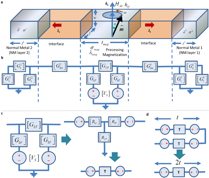
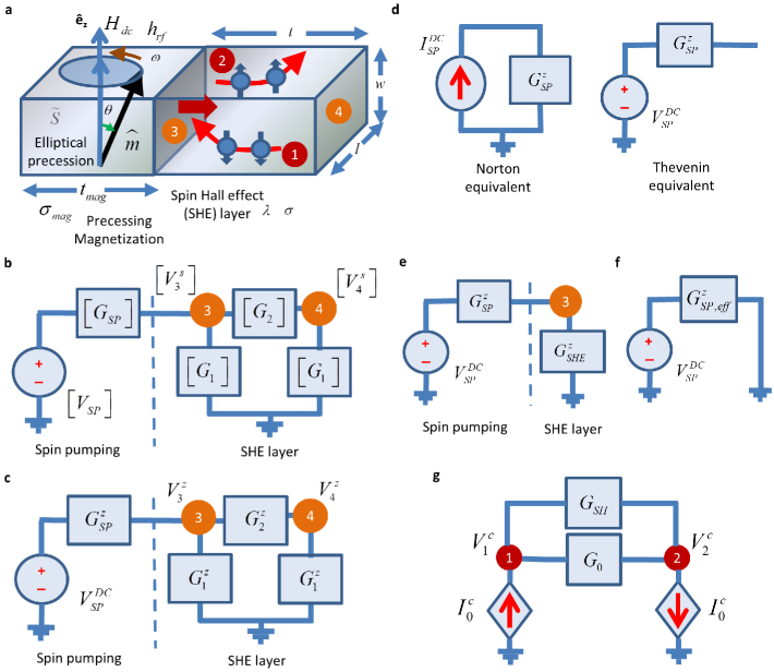
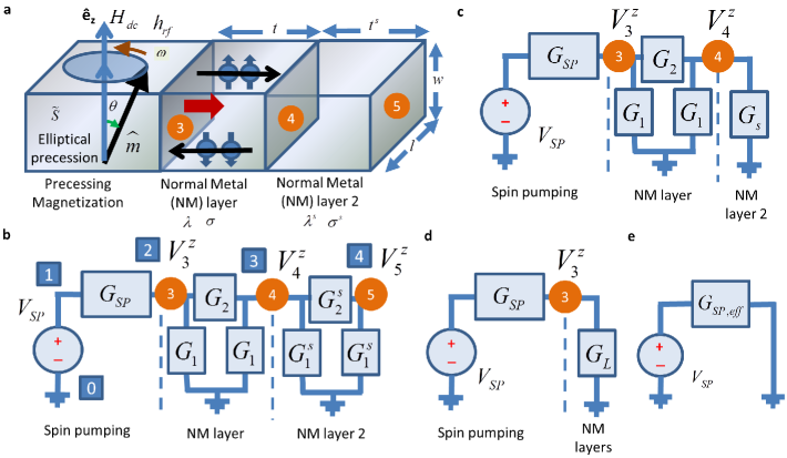
Figure 1 shows the spin circuit representation of spin pumping, with the conductances Imry and Landauer (1999); *RefWorks:1289; *RefWorks:1290 (after the necessary modifications Brataas et al. (2006); Srinivasan et al. (2014)) and spin voltage sources represented as follows.
| (3) |
| (4) |
| (5) |
| (6) |
and ,
where , , , , , , , ,
is the spin polarization of the FM, and are the FM-NM interface conductance and polarization, respectively, , , and are the spin diffusion length, conductivity, and thickness of the NM1(2) layer, respectively, , , and are the longitudinal spin diffusion length, conductivity, and thickness of the FM layer, respectively, and is the cross-sectional area.
The following points should be noted from the spin circuit representation of spin pumping in the Fig. 1: (1) We include the spin battery in the FM module since a magnet can be precessed without the connection of an NM module. (2) Figs. 1(c) and 1(d) explain (see the caption) that the spin battery appears at the interface only, which accords with the established physical concept in literature Tserkovnyak et al. (2005). (3) We consider the transverse components () of the conductances entirely at the FM-NM interface (), thus the transverse components of are . (4) We consider that the magnet is thick enough (compared to the transverse spin diffusion length , which is a few monolayers for the typical transition metals) so that the transmission spin mixing conductances are nearly zero, and thus we only consider the reflection spin mixing conductances Tserkovnyak et al. (2005). (5) For magnetic insulators Kajiwara et al. (2010); *RefWorks:992; *RefWorks:885; *RefWorks:1189; *RefWorks:991; *RefWorks:1017; *RefWorks:998, , , () represents the spin wave/magnon conductivity (diffusion length), and the transmission spin mixing conductances are exactly zero (i.e., the transverse components of and are exactly and , respectively).
Figure 2 shows the 3-component version of spin pumping and the generation of inverse spin Hall voltage in the transverse direction due to the symmetry involved in the system Mosendz et al. (2010a, b). The instantaneous spin pumping [Figure 2(b)] in matrix form can be represented by , where
| (7) |
| (8) |
, ( is the complex spin mixing conductance per unit area), is the frequency dependent elliptical precession factor due to thin magnetic film Ando et al. (2009), the components of
, , , and is the identity matrix.
The spin circuit representation of average spin pumping for a complete precession is depicted in the Fig. 2(c) with the voltage source (or the current source depicted in the Fig. 2(d)) represented by (). Thus . Note that first principles calculations and experiments have shown that the imaginary component of is negligible for metallic interfaces (i.e., ) Zwierzycki et al. (2005); Mosendz et al. (2010a); *RefWorks:813. , . From Fig. 2(d), . From Fig. 2(e), we get . Hence, we get
| (9) |
which matches the mathematical expression derived in literature Tserkovnyak et al. (2005). The above equation can be backcalculated to get the the bare spin mixing conductance with the inequality , since . Note that (and not the bare ) can be determined from the enhancement of damping in ferromagnetic resonance experiments Mosendz et al. (2010a); *RefWorks:813.
Figure 2(g) shows the charge circuit for the generation of inverse spin Hall voltage Hong et al. (2016) (), which also considers the conductance due to current shunting through the magnet, if it is metallic. The charge current sources in Fig. 2(g), depend on the spin potential difference between the nodes 3 and 4 in the Fig. 2(c) as , where , , and is the spin Hall angle Hong et al. (2016).
Applying KCL at node 1 of the charge circuit in Fig. 2(g), we get and hence
| (10) |
To calculate , we apply KCL at nodes 3 and 4 of the spin circuit in Fig. 2(c), and we get
| (11) |
where . From Equation (10), we get
| (12) |
which matches the mathematical expression derived in literature Mosendz et al. (2010a); *RefWorks:813.
Figure 3 shows spin pumping in two subsequent layers and the corresponding spin circuits to determine the effective spin mixing conductance of the whole structure. The spin conductance of the NM layer 2 in the Fig. 3(c) can be determined as where and the whole spin conductance of the two NM layers can be written as . Accordingly, we get
| (13) |
where and this expression matches the mathematical expression derived in literature Harii et al. (2012). For more complex multilayers, the analytical expression is tedious and this explains the prowess of the spin circuit approach. We can simply write a netlist (see the node numbers in squares in the Fig. 3(b)) as follows for the two layer case.
With a circuit solver, we can solve for (also the 3-component circuit in Fig. 2(b) and and the 4-component circuit in Fig. 1 can be solved in general) and using , we can determine the effective spin mixing conductance of the whole structure (shown in Fig. 3(e)) as
| (14) |
To summarize, we have developed the spin circuit representation of spin pumping and have shown that such representation accords to the established mathematical expressions in literature. Such circuits can be simply solved analytically and when more complex they can be solved programmatically to analyze and propose complex devices. We have not considered conductance for the interfacial Rashba-Edelstein effect at NM-NM interface Edelstein (1990); *RefWorks:1257; *RefWorks:1258 or any significant interfacial spin memory loss at FM-NM interface, on which (and also on spin diffusion length, spin Hall angle) there is controversy Fert and Lee (1996); *RefWorks:1042; *RefWorks:1316; *RefWorks:986; *RefWorks:1114; *RefWorks:1319; *RefWorks:1113; *RefWorks:1016; *RefWorks:983; *RefWorks:980. It needs to also carefully consider the low-thickness regime and the effect of magnetic proximity effect Huang et al. (2012); *RefWorks:1006; *RefWorks:1312; *RefWorks:1007; *RefWorks:988; *RefWorks:1323. The spin circuit presented here has immense consequence on the development of spintronic technology.
This work was supported by FAME, one of six centers of STARnet, a Semiconductor Research Corporation program sponsored by MARCO and DARPA.
References
- Silsbee et al. (1979) R. H. Silsbee, A. Janossy, and P. Monod, Phys. Rev. B 19, 4382 (1979).
- Mizukami et al. (2001a) S. Mizukami, Y. Ando, and T. Miyazaki, J. Magn. Magn. Mater. 226, 1640 (2001a).
- Mizukami et al. (2001b) S. Mizukami, Y. Ando, and T. Miyazaki, Jap. J. Appl. Phys. 40, 580 (2001b).
- Mizukami et al. (2002a) S. Mizukami, Y. Ando, and T. Miyazaki, Phys. Rev. B 66, 104413 (2002a).
- Mizukami et al. (2002b) S. Mizukami, Y. Ando, and T. Miyazaki, J. Magn. Magn. Mater. 239, 42 (2002b).
- Heinrich et al. (1987) B. Heinrich, K. B. Urquhart, A. S. Arrott, J. F. Cochran, K. Myrtle, and S. T. Purcell, Phys. Rev. Lett. 59, 1756 (1987).
- Urban et al. (2001) R. Urban, G. Woltersdorf, and B. Heinrich, Phys. Rev. Lett. 87, 217204 (2001).
- Platow et al. (1998) W. Platow, A. N. Anisimov, G. L. Dunifer, M. Farle, and K. Baberschke, Phys. Rev. B 58, 5611 (1998).
- Tserkovnyak et al. (2002a) Y. Tserkovnyak, A. Brataas, and G. E. W. Bauer, Phys. Rev. Lett. 88, 117601 (2002a).
- Tserkovnyak et al. (2002b) Y. Tserkovnyak, A. Brataas, and G. E. W. Bauer, Phys. Rev. B 66, 224403 (2002b).
- Tserkovnyak et al. (2005) Y. Tserkovnyak, A. Brataas, G. E. W. Bauer, and B. I. Halperin, Rev. Mod. Phys. 77, 1375 (2005).
- Costache et al. (2006) M. V. Costache, M. Sladkov, S. M. Watts, C. H. van der Wal, and B. J. van Wees, Phys. Rev. Lett. 97, 216603 (2006).
- Ando et al. (2011) K. Ando, S. Takahashi, J. Ieda, H. Kurebayashi, T. Trypiniotis, C. H. W. Barnes, S. Maekawa, and E. Saitoh, Nature Mater. 10, 655 (2011).
- Brouwer (1998) P. W. Brouwer, Phys. Rev. B 58, R10135 (1998).
- Büttiker et al. (1994) M. Büttiker, H. Thomas, and A. Prêtre, Z. Phys. B 94, 133 (1994).
- Kimura et al. (2007) T. Kimura, Y. Otani, T. Sato, S. Takahashi, and S. Maekawa, Phys. Rev. Lett. 98, 156601 (2007).
- Ando et al. (2008) K. Ando, S. Takahashi, K. Harii, K. Sasage, J. Ieda, S. Maekawa, and E. Saitoh, Phys. Rev. Lett. 101, 036601 (2008).
- Mosendz et al. (2010a) O. Mosendz, J. E. Pearson, F. Y. Fradin, G. E. W. Bauer, S. D. Bader, and A. Hoffmann, Phys. Rev. Lett. 104, 046601 (2010a).
- Mosendz et al. (2010b) O. Mosendz, V. Vlaminck, J. E. Pearson, F. Y. Fradin, G. E. W. Bauer, S. D. Bader, and A. Hoffmann, Phys. Rev. B 82, 214403 (2010b).
- Liu et al. (2011) L. Liu, T. Moriyama, D. C. Ralph, and R. A. Buhrman, Phys. Rev. Lett. 106, 036601 (2011).
- Liu et al. (2012) L. Liu, C. F. Pai, Y. Li, H. W. Tseng, D. C. Ralph, and R. A. Buhrman, Science 336, 555 (2012).
- Pai et al. (2012) C. F. Pai, L. Liu, Y. Li, H. W. Tseng, D. C. Ralph, and R. A. Buhrman, Appl. Phys. Lett. 101, 122404 (2012).
- Niimi et al. (2011) Y. Niimi, M. Morota, D. H. Wei, C. Deranlot, M. Basletic, A. Hamzic, A. Fert, and Y. Otani, Phys. Rev. Lett. 106, 126601 (2011).
- Niimi et al. (2012) Y. Niimi, Y. Kawanishi, D. H. Wei, C. Deranlot, H. X. Yang, M. Chshiev, T. Valet, A. Fert, and Y. Otani, Phys. Rev. Lett. 109, 156602 (2012).
- Niimi et al. (2014) Y. Niimi, H. Suzuki, Y. Kawanishi, Y. Omori, T. Valet, A. Fert, and Y. Otani, Phys. Rev. B 89, 054401 (2014).
- Laczkowski et al. (2014) P. Laczkowski, J. C. Rojas-Sánchez, W. Savero-Torres, H. Jaffrès, N. Reyren, C. Deranlot, L. Notin, C. Beigné, A. Marty, and J. P. Attané, Appl. Phys. Lett. 104, 142403 (2014).
- Wang et al. (2006) X. Wang, G. E. W. Bauer, B. J. van Wees, A. Brataas, and Y. Tserkovnyak, Phys. Rev. Lett. 97, 216602 (2006).
- Jiao and Bauer (2013) H. Jiao and G. E. W. Bauer, Phys. Rev. Lett. 110, 217602 (2013).
- Azevedo et al. (2005) A. Azevedo, L. H. Vilela-Leão, R. L. Rodríguez-Suárez, A. B. Oliveira, and S. M. Rezende, J. Appl. Phys. 97, 10C715 (2005).
- Saitoh et al. (2006) E. Saitoh, M. Ueda, H. Miyajima, and G. Tatara, Appl. Phys. Lett. 88, 182509 (2006).
- Onsager (1931a) L. Onsager, Phys. Rev. 37, 405 (1931a).
- Onsager (1931b) L. Onsager, Phys. Rev. 38, 2265 (1931b).
- Jacquod et al. (2012) P. Jacquod, R. S. Whitney, J. Meair, and M. Büttiker, Phys. Rev. B 86, 155118 (2012).
- Brataas et al. (2012) A. Brataas, Y. Tserkovnyak, G. E. W. Bauer, and P. J. Kelly, “Spin pumping and spin transfer,” in Spin Current, Vol. 17, edited by S. Maekawa, S. O. Valenzuela, E. Saitoh, and T. Kimura (Oxford University Press, 2012) pp. 87–135.
- Slonczewski (1996) J. C. Slonczewski, J. Magn. Magn. Mater. 159, L1 (1996).
- Berger (1996) L. Berger, Phys. Rev. B 54, 9353 (1996).
- Sun (2000) J. Z. Sun, Phys. Rev. B 62, 570 (2000).
- Stiles and Zangwill (2002) M. D. Stiles and A. Zangwill, Phys. Rev. B 66, 14407 (2002).
- Dyakonov and Perel (1971) M. I. Dyakonov and V. I. Perel, Sov. Phys. JETP Lett. 13, 467 (1971).
- Hirsch (1999) J. E. Hirsch, Phys. Rev. Lett. 83, 1834 (1999).
- Zhang (2000) S. Zhang, Phys. Rev. Lett. 85, 393 (2000).
- Murakami et al. (2003) S. Murakami, N. Nagaosa, and S. C. Zhang, Science 301, 1348 (2003).
- Sinova et al. (2004) J. Sinova, D. Culcer, Q. Niu, N. A. Sinitsyn, T. Jungwirth, and A. H. MacDonald, Phys. Rev. Lett. 92, 126603 (2004).
- Sinova et al. (2015) J. Sinova, S. O. Valenzuela, J. Wunderlich, C. H. Back, and T. Jungwirth, Rev. Mod. Phys. 87, 1213 (2015).
- Valenzuela and Tinkham (2006) S. O. Valenzuela and M. Tinkham, Nature 442, 176 (2006).
- Roy (2014) K. Roy, J. Phys. D: Appl. Phys. 47, 422001 (2014).
- (47) HSPICE, Circuit simulation software, Synopsys, www.synopsys.com.
- Rabaey et al. (2003) J. M. Rabaey, A. P. Chandrakasan, and B. Nikoliç, Digital Integrated Circuits (Pearson Education, 2003).
- Brataas et al. (2006) A. Brataas, G. E. W. Bauer, and P. J. Kelly, Phys. Rep. 427, 157 (2006).
- Srinivasan et al. (2014) S. Srinivasan, V. Diep, B. Behin-Aein, A. Sarkar, and S. Datta, “Modeling multi-magnet networks interacting via spin currents,” in Handbook of Spintronics, edited by Y. Xu, D. D. Awschalom, and J. Nitta (Springer Netherlands, Dordrecht, 2014) pp. 1–49.
- Hong et al. (2016) S. Hong, S. Sayed, and S. Datta, IEEE Trans. Nanotech. 15, 225 (2016).
- Harii et al. (2012) K. Harii, Z. Qiu, T. Iwashita, Y. Kajiwara, K. Uchida, K. Ando, T. An, Y. Fujikawa, and E. Saitoh, Key Eng. Mater. 508, 266 (2012).
- Brataas et al. (2002) A. Brataas, Y. Tserkovnyak, G. E. W. Bauer, and B. I. Halperin, Phys. Rev. B 66, 060404 (2002).
- Brataas et al. (2000) A. Brataas, Y. V. Nazarov, and G. E. W. Bauer, Phys. Rev. Lett. 84, 2481 (2000).
- Brataas et al. (2001) A. Brataas, Y. V. Nazarov, and G. E. W. Bauer, Eur. Phys. J. B 22, 99 (2001).
- Weiler et al. (2013) M. Weiler, M. Althammer, M. Schreier, J. Lotze, M. Pernpeintner, S. Meyer, H. Huebl, R. Gross, A. Kamra, J. Xiao, Y. T. Chen, H. Jiao, G. E. W. Bauer, and S. T. B. Goennenwein, Phys. Rev. Lett. 111, 176601 (2013).
- Imry and Landauer (1999) Y. Imry and R. Landauer, Rev. Mod. Phys. 71, S306 (1999).
- Landauer (1957) R. Landauer, IBM J. Res. Dev. 1, 223 (1957).
- Buttiker (1988) M. Buttiker, IBM J. Res. Dev. 32, 317 (1988).
- Kajiwara et al. (2010) Y. Kajiwara, K. Harii, S. Takahashi, J. Ohe, K. Uchida, M. Mizuguchi, H. Umezawa, H. Kawai, K. Ando, and K. Takanashi, Nature 464, 262 (2010).
- Heinrich et al. (2011) B. Heinrich, C. Burrowes, E. Montoya, B. Kardasz, E. Girt, Y. Y. Song, Y. Sun, and M. Wu, Phys. Rev. Lett. 107, 066604 (2011).
- Castel et al. (2012) V. Castel, N. Vlietstra, J. B. Youssef, and B. J. van Wees, Appl. Phys. Lett. 101, 132414 (2012).
- Kapelrud and Brataas (2013) A. Kapelrud and A. Brataas, Phys. Rev. Lett. 111, 097602 (2013).
- Sun et al. (2013) Y. Sun, H. Chang, M. Kabatek, Y. Y. Song, Z. Wang, M. Jantz, W. Schneider, M. Wu, E. Montoya, B. Kardasz, B. Heinrich, S. G. E. te Velthuis, S. H., and A. Hoffmann, Phys. Rev. Lett. 111, 106601 (2013).
- Zhou et al. (2013) Y. Zhou, H. Jiao, Y. Chen, G. E. W. Bauer, and J. Xiao, Phys. Rev. B 88, 184403 (2013).
- Wang et al. (2014) H. L. Wang, C. H. Du, Y. Pu, R. Adur, P. C. Hammel, and F. Y. Yang, Phys. Rev. Lett. 112, 197201 (2014).
- Ando et al. (2009) K. Ando, T. Yoshino, and E. Saitoh, Appl. Phys. Lett. 94, 152509 (2009).
- Zwierzycki et al. (2005) M. Zwierzycki, Y. Tserkovnyak, P. J. Kelly, A. Brataas, and G. E. W. Bauer, Phys. Rev. B 71, 064420 (2005).
- Edelstein (1990) V. M. Edelstein, Solid State Commun. 73, 233 (1990).
- Sánchez et al. (2013) J. C. R. Sánchez, L. Vila, G. Desfonds, S. Gambarelli, J. P. Attané, J. M. D. Teresa, C. Magén, and A. Fert, Nature Commun. 4, 2944 (2013).
- Zhang et al. (2015a) W. Zhang, M. B. Jungfleisch, W. Jiang, J. E. Pearson, and A. Hoffmann, J. Appl. Phys. 117, 17C727 (2015a).
- Fert and Lee (1996) A. Fert and S. F. Lee, Phys. Rev. B 53, 6554 (1996).
- Kovalev et al. (2002) A. A. Kovalev, A. Brataas, and G. E. W. Bauer, Phys. Rev. B 66, 224424 (2002).
- Nguyen et al. (2014) H. Y. T. Nguyen, W. P. Pratt, and J. Bass, J. Magn. Magn. Mater. 361, 30 (2014).
- Feng et al. (2012) Z. Feng, J. Hu, L. Sun, B. You, D. Wu, J. Du, W. Zhang, A. Hu, Y. Yang, and D. M. Tang, Phys. Rev. B 85, 214423 (2012).
- Rojas-Sánchez et al. (2014) J. C. Rojas-Sánchez, N. Reyren, P. Laczkowski, W. Savero, J. P. Attané, C. Deranlot, M. Jamet, J. M. George, L. Vila, and H. Jaffrès, Phys. Rev. Lett. 112, 106602 (2014).
- Liu et al. (2014) Y. Liu, Z. Yuan, R. J. H. Wesselink, A. A. Starikov, and P. J. Kelly, Phys. Rev. Lett. 113, 207202 (2014).
- Chen and Zhang (2015) K. Chen and S. Zhang, Phys. Rev. Lett. 114, 126602 (2015).
- Zhang et al. (2015b) W. Zhang, W. Han, X. Jiang, S. H. Yang, and S. S. P. Parkin, Nature Phys. 11, 496 (2015b).
- Zhang et al. (2013) W. Zhang, V. Vlaminck, J. E. Pearson, R. Divan, S. D. Bader, and A. Hoffmann, Appl. Phys. Lett. 103, 242414 (2013).
- Boone et al. (2015) C. T. Boone, J. M. Shaw, H. T. Nembach, and T. J. Silva, J. Appl. Phys. 117, 223910 (2015).
- Huang et al. (2012) S. Y. Huang, X. Fan, D. Qu, Y. P. Chen, W. G. Wang, J. Wu, T. Y. Chen, J. Q. Xiao, and C. L. Chien, Phys. Rev. Lett. 109, 107204 (2012).
- Lu et al. (2013) Y. M. Lu, Y. Choi, C. M. Ortega, X. M. Cheng, J. W. Cai, S. Y. Huang, L. Sun, and C. L. Chien, Phys. Rev. Lett. 110, 147207 (2013).
- Lim et al. (2013) W. L. Lim, N. Ebrahim-Zadeh, J. C. Owens, H. G. E. Hentschel, and S. Urazhdin, Appl. Phys. Lett. 102, 162404 (2013).
- Yang et al. (2014) Y. Yang, B. Wu, K. Yao, S. Shannigrahi, B. Zong, and Y. Wu, J. Appl. Phys. 115, 17C509 (2014).
- Zhang et al. (2015c) W. Zhang, M. B. Jungfleisch, W. Jiang, Y. Liu, J. E. Pearson, S. G. E. te Velthuis, A. Hoffmann, F. Freimuth, and Y. Mokrousov, Phys. Rev. B 91, 115316 (2015c).
- Caminale et al. (2016) M. Caminale, A. Ghosh, S. Auffret, U. Ebels, K. Ollefs, F. Wilhelm, A. Rogalev, and W. E. Bailey, Phys. Rev. B 94, 014414 (2016).