Ultralow Energy Analog Straintronics Using Multiferroic Composites
Abstract
Electric field-induced magnetization switching in multiferroics holds profound promise for ultra-low-energy computing in beyond Moore’s law era. Bistable nanomagnets in the multiferroics are usually deemed to be suitable for storing a binary bit of information and switching between the two stable states allows us to process digital information. However, it requires to process continuous analog signals too for seamless integration of nanomagnetic devices in our future information processing systems. Here, we show that it is possible to harness the analog nature in the magnetostrictive nanomagnets, contrary to writing a digital bit of information. By solving stochastic Landau-Lifshitz-Gilbert equation of magnetization dynamics at room-temperature, we demonstrate such possibility and show that there exists a transistor-like high-gain region in the input-output characteristics of the magnetostrictive nanomagnets in strain-mediated multiferroic composites. This can be the basis of ultra-low-energy analog and mixed signal precessing in our future information processing systems and it eliminates the requirement of using charge-based transistors.
Index Terms:
Analog signal processing, energy-efficient design, multiferroics, nanomagnets.I Introduction
The invention and development of traditional charge-based transistor electronics has been a story of great success [1], however, fundamental limits hindrance the further progress [2]. In quest of energy-efficient computing, electron’s spin-based counterpart, so-called spintronics, has been widely studied in the context of nanomagnets [3, 4, 5, 6, 7, 8, 9, 10, 11, 12]. Nanomagnets with two stable states separated by an energy barrier are usually envisaged by the spintronics community for non-volatile binary switching [6]. While switching the magnetization direction between its two stable states allows us to process information digitally (encoded as 0 and 1) [6, 13, 14], it requires to perform analog signal processing [15] using the inherently bistable nanomagnets for seamless integration of nanomagnetic devices on a chip. The analog signal processing capability is sometimes fundamentally necessary too, e.g., while processing natural signals that are attenuated in the environment and it needs amplification before further processing in digital domain [15]. Such voltage gain is also necessary for error resiliency in digital integrated circuits [16].
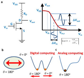
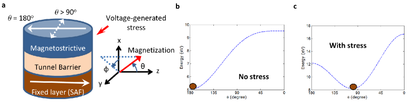
Figure 1a depicts the basic notion of processing analog signals using traditional transistors [15]. When the input voltage is higher than the threshold voltage, a significant amount of current starts to flow and when a sufficient input voltage is applied, the current saturates. While the high- and low-state encapsulate a binary bit of digital information, the transition region in between is gradual but has a high slope, where we can bias a continuous analog input voltage and generate an output voltage with a voltage gain. Figure 1b shows the potential landscape of a nanomagnet with two anti-parallel stable states storing a binary bit of information and . For digital computing, we need to switch the magnetization between these two stable states. However, for analog computing, we select one potential well to operate by making the potential landscape monostable since we want to restrict abrupt switching from one stable state to another. This is depicted in the Fig. 1c with a monostable potential well.
Recently, it is shown that electric field induced magnetization switching in strain-mediated multiferroic composites, i.e., a piezoelectric layer strain-coupled with a magnetostrictive nanomagnet [17, 18, 19], dissipates a miniscule amount of energy of 1 attojoule (aJ) in sub-nanosecond switching delay at room-temperature [6, 20, 21, 22, 23, 24]. Also, the Landauer limit of energy dissipation [4] can be achieved in these magnetostrictive nanomagnets [25]. The induced stress anisotropy in magnetostrictive nanomagnets has been experimentally demonstrated too [26, 27, 28, 29, 30, 31, 32]. With voltage generated stress in a magnetostrictive nanomagnet, the potential landscape of the nanomagnet can be modulated and thereby here we show that it is possible to harness the analog signal processing capability [33, 34, 35]. By solving stochastic Landau-Lifshitz-Gilbert equation [36, 37, 38] of magnetization dynamics in the presence of room-temperature thermal fluctuations, we show that a continuous rotation of magnetization is possible and a transistor-like high-gain region in the input-output characteristics of these multiferroic composite devices can be achieved [33, 34, 35]. A voltage gain of 50 can be achieved while dissipating only 0.1 aJ/cycle at 1 GHz frequency.
Being able to perform analog signal processing too using these multiferroic devices will facilitate seamless integration of nanomagnetic devices in the same manufacturing process on chips and will eliminate transistors as supporting devices. Therefore, this is key to the success of building energy-efficient technology based on these multiferroic devices.
II Model: Solution of stochastic Landau-Lifshitz-Gilbert (LLG) equation of magnetization dynamics in the presence of thermal fluctuations
We adopt the standard spherical coordinate system (see Fig. 2a) to solve the stochastic LLG equation of magnetization dynamics. The magnets are lying on the - plane, and is the out-of-plane direction. In standard spherical coordinate system, is the polar angle and is the azimuthal angle.
First, we will consider that a magnetostrictive nanomagnet on which an effective magnetic field is exerted from the fixed layer in an magnetic tunnel junction (MTJ) structure (see Fig. 2a). This structure is used to explain the concepts behind the continuous rotation of magnetization in the magnetostrictive nanomagnet with the application of stress. There is a high gain region in the stress versus the mean orientation of magnetization, where we can bias an AC signal. Therefore, stress is time-dependent in the formulation.
Then we will consider a dipole-coupled structure between the magnetostrictive nanomagnet in a multiferroic composite and the free layer of an magnetic tunnel junction (see Fig. 3a). This is a more complicated and realistic design since read unit (magnetic tunnel junction) and write unit (multiferroic composite) are separated here so that the best materials for the magnetostrictive and free layer nanomagnets can be utilized.
II-A A magnetostrictive nanomagnet with an effective field from a fixed layer
Figure 2a shows a single-domain magnetostrictive nanomagnet, on which an effective field is exerted from the fixed layer (synthetic antiferromagnetic (SAF) layer [39]). This is the case for which continuous rotation of magnetization with stress is shown by solving stochastic LLG simulation.
We can write the total energy of the polycrystalline magnetostrictive nanomagnet as the sum of three energies – the shape anisotropy energy, the stress anisotropy energy, and the anisotropy energy due to an effective field from the fixed layer in the direction (see Fig. 2a) – as follows:
| (1) |
where
| (2) | ||||
| (3) | ||||
| (4) | ||||
| (5) |
is the saturation magnetization, is the Stoner-Wohlfarth switching field [40], is the out-of-plane demagnetization field [40], is the mth () component of the demagnetization factor, which depends on the dimensions of the nanomagnet [41] (), is the volume of the magnetostrictive nanomagnet, is the magnetostriction coefficient of the magnetostrictive nanomagnet [40], is the stress at time , and is the effective field exerted by the fixed layer.
Note that a negative product will favor alignment of the magnetization along the minor axis (-axis) and according to our convention, in a material having positive (Terfenol-D i.e., TbDyFe, Galfenol i.e., FeGa), a sufficiently high compressive stress that can overcome the in-plane shape-anisotropic barrier will rotate the magnetization toward the in-plane hard axis (, ). In Fig. 2c, note that the minimum energy position is not exactly , which is due to the effective field exerted from the fixed layer on the magnetostrictive nanomagnet to make the potential landscape monostable (see Fig. 2b).
The magnetization M of the nanomagnet has a constant magnitude but a variable direction, so that we can represent it by a vector of unit norm where is the unit vector in the radial direction in spherical coordinate system represented by (,,). The other two unit vectors in the spherical coordinate system are denoted by and for and rotations, respectively.
The effective field and torque acting on the magnetization due to gradient of potential landscape can be expressed as
| (6) | ||||
| (7) |
where
| (8) |
The effect of random thermal fluctuations is incorporated via a random magnetic field
| (9) |
where () are the three components of the random thermal field in Cartesian coordinates. We assume the properties of the random field as described in Ref. [38]. The random thermal field can be written as [38]
| (10) |
where is the dimensionless phenomenological Gilbert damping parameter, is the gyromagnetic ratio for electrons, , is proportional to the attempt frequency of the thermal field, is a Gaussian distribution with zero mean and unit variance, is the Boltzmann constant, and is temperature.
The thermal field and corresponding torque acting on the magnetization can be written, respectively as
| (11) | ||||
| (12) |
where
| (13) | ||||
| (14) |
The magnetization dynamics under the action of the torques and is described by the stochastic Landau-Lifshitz-Gilbert (LLG) equation [36, 37, 38] as follows.
| (15) |
Solving the above equation analytically, we get the following coupled equations of magnetization dynamics for and :
| (16) |
| (17) |
We need to solve the above two coupled equations numerically to track the trajectory of magnetization over time, in the presence of thermal fluctuations.
The energy dissipated in the nanomagnet due to Gilbert damping can be expressed as , where is the time period when the input signal is active and is the power dissipated at time per unit volume given by
| (18) |
Thermal field with mean zero does not cause any net energy dissipation but it causes variability in the energy dissipation by scuttling the trajectory of magnetization.
Initial fluctuation of magnetization.– When the magnetization direction is exactly along the easy axis, i.e., ( or ), the torque acting on the magnetization given by Equation (7) becomes zero. That is why only thermal fluctuations can deflect the magnetization vector exactly from the easy axis. Considering the situation when , from Equations (16) and (17), we get [22]
| (19) |
| (20) |
From the Equation (20), we notice clearly that the thermal fluctuations can deflect the magnetization exactly from the easy axis since the time rate of change of is non-zero in the presence of thermal fluctuations. Note that does not depend on the component of the random thermal field along the -axis, i.e. , which is a consequence of having -axis as the easy axis of the nanomagnet. However, once the magnetization direction is even slightly deflected from the easy axis, all three components of the random thermal field along the -, -, and -direction would come into play.
II-B A magnetostrictive nanomagnet magnetically coupled with a free layer with an effective field exerted from a fixed layer
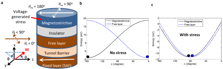
Figure 3a shows a magnetostrictive nanomagnet lying on the - plane and it is dipole coupled with the free layer in an MTJ. The strong dipole coupling makes the potential landscapes of both the nanomagnets monostable as shown in the Fig. 3b. The fixed layer can exert an effective field on the free layer, however, that is not necessary to make the potential landscape of the magnetostrictive nanomagnet monostable, as required for the case in Fig. 2a. Such magnetically coupled design has been presented in Ref. [42] in the context of separating read and write units for digital computing purposes, however, as depicted in the Fig. 1, there is difference in the potential landscapes of the nanomagnets for analog computing.
The magnetization () of the magnetostrictive (free layer) nanomagnet has a constant magnitude but a variable direction, so that we can represent it by a vector of unit norm () where is the unit vector in the radial direction in spherical coordinate system represented by (,,). The other two unit vectors corresponding to the polar angle and the azimuthal angle are and , respectively. We will use the subscripts and to denote any parameter for the magnetostrictive nanomagnet and the free layer nanomagnet, respectively.
While there are two nanomagnets (magnetostrictive and free layer) having a dipole coupling between them (see Fig. 3a), stress is generated only on the magnetostrictive nanomagnet. Hence we have additional stress anisotropy to consider for the magnetostrictive nanomagnet. Also, we consider that the fixed layer in general exerts an effective field on the free layer. The potential energies of the single-domain polycrystalline magnetostrictive nanomagnet and the free layer nanomagnet can be expressed, respectively, as
| (21) |
and
| (22) |
where
| (23) | ||||
| (24) | ||||
| (25) |
| (26) | ||||
| (27) | ||||
| (28) |
| (29) |
where is the saturation magnetization of the magnetostrictive (free layer) nanomagnet, is the Stoner-Wohlfarth switching field [40] for the magnetostrictive (free layer) nanomagnet, is the out-of-plane demagnetization field [40] for the magnetostrictive (free layer) nanomagnet, is the component of the demagnetization factor for the magnetostrictive (free layer) nanomagnet along -direction, which depends on the nanomagnet’s dimensions [40, 41], () is the volume of the magnetostrictive (free layer) nanomagnet, is the magnetostrictive coefficient of the single-domain magnetostrictive nanomagnet [40], is the stress on the magnetostrictive nanomagnet at time , and is the effective field exerted by the fixed layer on the free layer, and is the center-to-center distance between the nanomagnets.
Note that the product of magnetostrictive coefficient and stress needs to be negative in sign so that the generated stress-anisotropy can beat the shape-anisotropy to rotate the magnetization of the magnetostrictive nanomagnet. As the magnetization of the magnetostrictive nanomagnet rotates upon application of stress, the magnetization of the free layer nanomagnet does also rotate due to the dipole coupling between the nanomagnets. An effective field is exerted from the fixed layer on the free layer to keep the respective orientations of the magnetostrictive nanomagnet and the free layer intact, i.e., when stress is removed, the magnetostrictive nanomagnet should be pointing to and free layer’s magnetization should be pointing to (see Fig. 3b).
We can write the LLG equations for the individual nanomagnets following the Equation (15), and we will also use the corresponding terms in the Equations (13) and (14) and for the magnetostrictive (free layer) nanomagnet, as the phenomenological damping parameter of the magnetostrictive (free layer) nanomagnet, and . After solving the two LLG equations, we get the following coupled equations for the dynamics of and :
| (30) |
| (31) |
and the following coupled equations for the dynamics of and :
| (32) |
| (33) |
where
| (34) |
| (35) | ||||
| (36) |
The magnetization dynamics of the two nanomagnets represented by the Equations (30), (31), (32), and (33), are coupled through the dipole coupling [see Equation (29)]. These coupled equations are solved numerically to track the trajectories of the two magnetizations over time.
The individual internal energy dissipation in the magnetostrictive nanomagnet and the free layer due to Gilbert damping and , respectively can be expressed following the prescription in Equation (18). We sum up these two internal energy dissipations and to get the total energy dissipation in the nanomagnets. Since the magnetizations of the two magnetically coupled nanomagnets rotate quite concomitantly, a single time period when the input signal is active is sufficient.
Initial fluctuations of the magnetizations.– When the magnetization direction of the magnetostrictive nanomagnet and the free layer’s magnetization are exactly along and , respectively (Fig. 3b), the torque acting on the magnetizations become zero. That is why only thermal fluctuations can deflect the magnetization vector from this lockjam. For the magnetostrictive nanomagnet, when , we can derive the following:
| (37) |
| (38) |
Similarly, for the free layer, when , we can derive the following:
| (39) |
| (40) |
From the Equations (38) and (40), we notice clearly that the thermal fluctuations can deflect the magnetizations exactly from their respective easy axis since the time rate of change of and is non-zero in the presence of thermal fluctuations. The sign of the rates of change of and are in the opposite direction, which signify that decreases from and increases from with random thermal fluctuations, facilitating the rotation of the magnetically coupled magnetizations. Note that does not depend on the component of the random thermal field along the -axis, which is a consequence of having -axis as the easy axis of the nanomagnet. However, once the magnetization direction is even slightly deflected, all three components of the random thermal field along the -, -, and -direction would come into play.
It should be pointed out that the orientations of the magnetostrictive nanomagnet and the free layer are not exactly along and , due to thermal fluctuations. The mean deflection of the magnetizations due to room-temperature (300 K) thermal fluctuations, when no stress is applied, is . This is a bit lower than that of the case for Fig. 2b (mean deflection of magnetization around is ), due to the strong dipole coupling between the magnetostrictive nanomagnet and the free layer in Fig 3 for the same dimensions of the nanomagnets. On the contrary, such strong magnetic dipole coupling can help reducing the dimensions of the nanomagnets.
III Material parameters and device dimensions
The magnetostrictive nanomagnet is made of polycrystalline Terfenol-D and it has the following material properties – saturation magnetization (): 8105 A/m, Gilbert damping parameter (): 0.1, Young’s modulus (Y): 80 GPa, magnetostrictive coefficient (): +9010-5, and Poisson’s ratio (): 0.3 (Refs. [43, 44, 45, 46, 6, 23, 22, 20, 21, 13, 14]) For the magnetically-coupled structure (Fig. 3a), the free layer nanomagnet is made of widely used CoFeB, which has the following material properties – Gilbert damping parameter (): 0.01, saturation magnetization (): 8105 A/m [47].
For the piezoelectric layer, we use lead magnesium niobate-lead titanate (PMN-PT), which has a dielectric constant of 1000, =–3000 pm/V, and =1000 pm/V [30]. The piezoelectric layer’s thickness =50 nm (similar dimension is used in Ref. [23]). Using low-thickness piezoelectric layers [e.g., 100 nm of PMN-PT [48]] avoiding any substrate clamping effect [49, 48, 50] requires further experimental efforts. There are other multiferroic composites, e.g., Ni/PMN-PT [28, 51, 52], FeGaB/PMN-PT [53], CoFe/PMN-PT [30], CoFeB/PMN-PT [54, 31, 55], /PMN-PT [56], /PMN-PT [57, 58], however, Terfenol-D/PZN-PT [27] or Terfenol-D/PMN-PT [59] composites possess superior material parameters leading to high magnetoelectric coupling. FeGaB/PMN-PT composite has also high magnetoelectric couplings similar to Terfenol-D/PMN-PT.
For the magnetic tunnel junction in the magnetically-coupled structure (Fig. 3a), the resistance-area (RA) product (for parallel orientation), and tunneling magnetoresistance (TMR) are assumed to be 175 k- and 300% [60], respectively. MTJs with RA product as low as 4.3 - (Ref. [61]) and 1000% TMR with half-metals [62] are plausible.
The dimensions of the single-domain nanomagnets are chosen as , [41, 63] and the center-to-center distance between the nanomagnets in the magnetically-coupled structure (Fig. 3a) is . We choose the dimensions of the nanomagnet such that it has always a single ferromagnetic domain [41, 63]. (At higher dimensions, there are issues like inhomogeneous magnetization, buckling instability, nonuniform magnetization reversal, vortex dynamics etc. [64, 65, 66, 67, 68, 69].) This allows us to use the so-called macrospin model, which is valid at low dimensions [70, 71, 72], as chosen here.
IV Simulation Results and Discussions
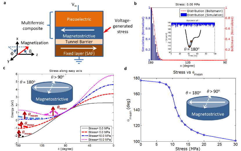
Figure 4a shows a multiferroic composite (piezoelectric layer strain-coupled with a magnetostrictive nanomagnet) and a fixed magnetization layer separated by a tunnel barrier e.g., Magnesium Oxide (MgO) [73, 74, 60, 75]. An input voltage generates strain in the piezoelectric layer and the strain is elastically transferred to the magnetostrictive nanomagnet generating a stress anisotropy in it. This additional anisotropy can rotate the magnetization of the magnetostrictive nanomagnet [6]. The rotation of magnetization can be detected using tunneling magnetoresistance measurement (in magnetic tunnel junctions (MTJs) [39]) with respect to the magnetization of the fixed layer. The fixed layer is implemented as a synthetic antiferromagnetic (SAF) layer [39], which can be designed in a way to exert a field on the magnetostrictive nanomagnet to make the potential landscape monostable as shown in the Fig. 1c. A magnetically coupled design between the multiferroic composite (write unit) and the MTJ (read unit) separating the write and read units [42] will be presented in the Fig. 5a later. The layers are shown as rectangular slabs, but they could be of any anisotropic shape like elliptical cylinders as we have used here.
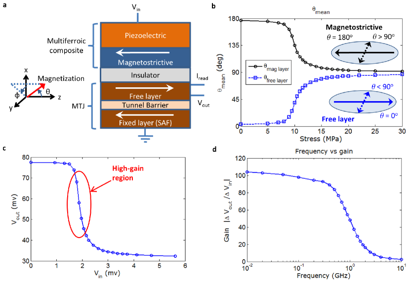
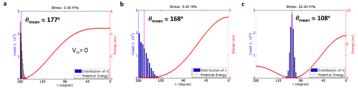
Figure 4b shows the room-temperature (300 K) distribution of magnetization (polar angle ) since magnetization is fluctuating due to thermal agitations around . The model utilized to determine this distribution is the stochastic Landau-Lifshitz-Gilbert (LLG) equation [38] of magnetization dynamics as described earlier in the presence of thermal fluctuations (incorporated as a random thermal field in the LLG equation) and it matches the Boltzmann distribution (see Fig. 4b) signifying the validity of our model. As voltage generated compressive stress is built on the magnetostrictive nanomagnet, it modifies the potential landscape of the nanomagnet and the mean orientation of magnetization () varies continuously due to thermal fluctuations as depicted in the Figs. 4c and 4d. When a sufficient compressive stress is applied, the magnetization comes near . A few distributions for different stresses calculated from stochastic LLG are shown in the Fig. 9 later.
Note that the azimuthal angle can be either or (both correspond to magnet’s plane) as depicted by the bidirectional arrow in Fig. 4c when reaches around . The azimuthal angle is imperative to consider since stress rotates magnetization out of magnet’s plane and a slight out-of-plane excursion can create a high torque on the magnetization due to high out-of-plane demagnetization field of the thin nanomagnet leading to an increase of switching speed by a couple of orders in magnitude to sub-nanosecond [22]. In general the azimuthal angle has also a distribution due to thermal fluctuations [22], however, due to the effective field exerted by the fixed layer on the magnetostrictive nanomagnet making the potential landscape monostable, the -distribution is quite quenched and it facilitates the match with the Boltzmann distribution in Fig. 4b considering only the -space.
In Fig. 5a, compared to the Fig. 4a, we have introduced a dipole coupled free layer so that suitable materials can be utilized for both the magnetostrictive layer of the multiferroic composite and the free layer of the MTJ independently. For the magnetostrictive layer, materials with high magnetostriction coefficient (Terfenol-D, Galfenol, i.e., FeGa) should be used, while for the free layer, relevant materials e.g., CoFeB, half-metals need to be used to achieve a high tunneling magnetoresistance (TMR) [73, 74, 60, 75, 62]. Although multiferroic composites employing CoFe [30, 31] is possible, with the advent of half-metal based MTJs [62] leading to even higher TMR than that of using CoFeB and the requirement of using materials with higher magnetostriction coefficient than that of CoFeB leading to a lower operating voltage (and therefore a lower energy dissipation), clearly establishes the requirement to separate the read and write units. Note that the insulator does not aid in input-output isolation for logic design purposes, since the insulating piezoelectric layer with much higher resistivity makes the input-output isolation inherent in these multiferroic devices [13]. Rather than using dipolar coupling, exchange-coupled magnets can be also utilized, as mentioned in Ref. [42].
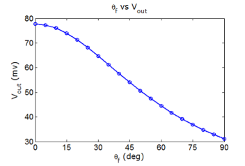
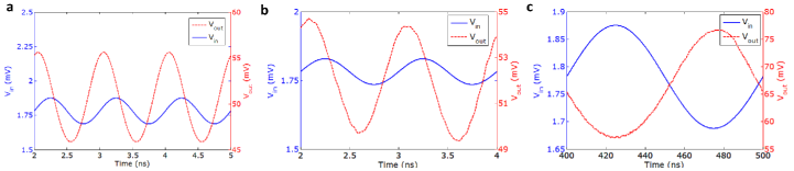
Figure 5b depicts that the magnetizations of the magnetostrictive nanomagnet and the free layer rotate concomitantly upon application of stress on the magnetostrictive nanomagnet. The model for this simulation has been described in the Section II. Since the design of the fixed layer (a synthetic antiferromagnetic layer) may not be very precise, an effective field of 10% of the free layer’s anisotropy field is assumed to be exerted on the free layer. (It also aids to keep the initial orientations of the magnetizations of the magnetostrictive nanomagnet and the free layer, when stress is withdrawn from the magnetostrictive nanomagnet.) Therefore, when a sufficient high stress is applied, the magnetization of the magnetostrictive nanomagnet comes to and not to exactly . At around , the magnetizations of the magnetostrictive nanomagnet and the free layer orient anti-parallel in -space. Note that the insulator thickness separating the magnetostrictive nanomagnet and the free layer is optimized since at higher thicknesses the magnetizations do not quite rotate concomitantly and at lower thicknesses, the high coupling rotates magnetizations out-of-plane leading to precessional motion [42].
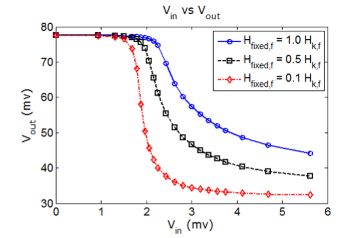
Figure 5c shows the input-output characteristics of the amplifier. The Appendices A and C describe the MTJ characteristics to extract the magnetization orientation versus output voltage relationship and the input voltage versus stress relationship, respectively. This input-output characteristics is similar to the transistor input-output characteristics having a high-gain region. This characteristics considers 10% of the free layer’s anisotropy field to be exerted on the free layer by the fixed layer, however, the gain remains similar when no field is exerted from the fixed layer. If the exerted field from the fixed layer increases significantly, the gain of the amplifier reduces (see Fig. 11 later). No effective field is considered to be exerted on the magnetostrictive layer by the fixed layer since it is 40 nm away [42]. The amplifier characteristics shown in the Fig. 5c signify that both the DC level enhancement and AC signal gain can be achieved simultaneously and the MTJ characteristics (see Fig. 8) aids in achieving it. The output voltage level can be adjusted by changing the read current and resistance-area product of the MTJ (by changing the tunnel barrier thickness) [60, 75]. To obtain a current source, the structure in Fig. 5a can be utilized, while biasing the MTJ using a constant voltage source (see Fig. 6). Note that the dipole-coupled design in the Fig. 5a achieves much better linearity in the high gain region compared to the case in the Fig. 4a. Fig. 5d plots the frequency dependence of gain. An AC voltage of different frequencies is applied at the input and the output voltage is extracted to determine the gain. This characteristics is similar to the transistor characteristics that at high frequency the gain reduces [15]. See Fig. 10 later for detailed simulations in this regard.
The energy dissipation for the amplifier presented in the Fig. 5 turns out to be 0.1 attojoule/cycle at 1 GHz frequency (see Appendix D). The experimental efforts on these multiferroic devices have demonstrated the existence of stress anisotropy and the stochastic LLG equation of magnetization dynamics used here is a standard tool to benchmark experimental results. Utilizing piezoelectric layers of low thickness ( 100 nm) avoiding any substrate clamping effect, which needs to be tackled [48, 49], while retaining high piezoelectric coefficients will allow us to operate these devices at few millivolts incurring miniscule amount of energy dissipation and therefore possibly by energy harvesting [76]. This is about 2-3 orders of magnitude less energy dissipation than the traditional charge based transistors operating at 1 Volt. Also, these multiferroic devices have advantage that these are voltage-controlled devices rather than current-controlled and the presence of thick piezoelectric layer leads to a miniscule leakage unlike the case of traditional transistors. The area and the frequency of operation for these devices can be further improved by using interface and exchange coupled systems, perpendicular anisotropy [77, 78] etc.
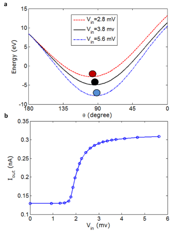
Figure 6 shows a characteristics of a current source (e.g., in Fig. 5a) using the strain-mediated multiferroic devices. Fig. 6a depicts the operating principle of building the current source. When sufficiently high input voltages are applied, the potential landscapes go deeper around and magnetization comes close to . To obtain a current source, the structure in Fig. 5 can be utilized, while biasing the MTJ using a constant voltage source . Fig. 6b shows the stochastic LLG simulation results of the current source using mV. This is similar to the transistor characteristics driven in saturation that provides almost constant currents [15]. It should be mentioned that we need to consider the characteristics of the current source while connecting to a load depending on the load resistance. The input resistance of the current source can be increased by increasing the resistance-area product or the area of the MTJ for the current source.
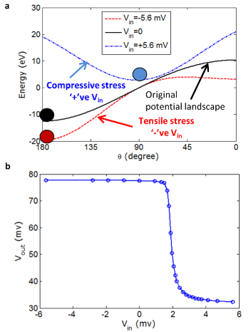
Figure 7 shows a characteristics of a rectifier using the strain-mediated multiferroic devices. Fig. 7a depicts the operating principle of building the rectifier. The magnetization of the magnetostrictive nanomagnet gets more confined in the potential landscape when a negative input voltage is applied, while a sufficiently high positive input voltage makes the potential landscape monostable around as depicted earlier in Fig. 5. Fig. 7b shows the stochastic LLG simulation results of the rectifier depicting two different output voltage levels when input voltages of different polarities are applied. The degree of rectification increases with TMR. Such DC voltage level conversion may be required for different signal processing tasks [15, 16].
V Conclusions
In conclusion, we have demonstrated an intriguing feature of harnessing analog nature in inherently digital nanomagnets utilizing energy-efficient piezoelectric-magnetostrictive multiferroic composites. This eliminates the use of cumbersome and energy-consuming magnetic field, which can be applied along the hard-axis of a shape-anisotropic nanomagnet to rotate its magnetization. Different methodologies employing different ways to apply stress modulating the potential landscape of the magnetostrictive nanomagnets can be also possible to achieve the similar characteristics described here. Harnessing the transistor-like characteristics for analog signal processing tasks using these energy-efficient multiferroic devices apart from digital switching makes these devices very promising to be utilized in our future information processing systems.
Appendix A Free layer’s magnetization orientation versus output voltage relation
For the dipole-coupled structure as in the Fig. 3 (Fig. 5), the conductance of the magnetic tunnel junction (MTJ) can be written as a function of the free layer’s magnetization orientation as [79]
| (41) |
where , , and () is the spin polarization of free (fixed) layer. The quantity can be expressed as
| (42) |
where and . The tunneling magnetoresistance TMR is expressed as
| (43) |
and it is related to as
| (44) |
Figure 8 shows the output voltage from the MTJ as a function of the free layer’s magnetization orientation with the following parameters: TMR = 300%, and resistance-area product - (Ref. [60]), where , and is the cross-sectional area of the junction. Although Ref. [60] uses CoFe and TMR=300% is achieved at low temperature, using CoFeB the TMR can be as high as 604% (Ref. [80]). Instead of using CoFe/CoFeB or Fe for the fixed/free layers [60, 75], half-metals [62] can produce TMR as high as 1000%. Also low resistance-area product as low as - (Ref. [61]) by lowering the MgO tunneling barrier thickness [75] is plausible. Note that we have used an elliptical cross-section for the cross-sectional area and we have utilized a read current nA. The voltage across the MTJ is only tens of millivolts and the bias dependence [79, 81, 82] of MTJ is not assumed. With bias dependence, TMR reduces a bit, however, with half-metals much higher TMR can be achieved anyway. Note that MTJ capacitance should be low enough so that it can follow high frequencies. There are experimental evidences of MTJ operation at more then 1 GHz [61, 83] and spin-transfer-torque switching with 50 ps pulse using spin-valve and giant-magnetoresistance (GMR) [84].
Appendix B Design of the fixed layer
The fixed layer in the Figs. 4a and 5a is shown as a single layer for brevity, however, the design of such layer constitutes of multiple layers [39] and such structure is routinely experimentally realized to build magnetic tunnel junctions (MTJs) [61, 85]. The fixed layer constitutes a synthetic antiferromagnetic (SAF) layer with a Ru spacer and a PtMn antiferromagnetic pinning layer [39, 61, 85]. A sample thickness values of such structure are PtMn(20 nm)/CoFe(2.3 nm)/Ru(0.85 nm)/CoFeB(2.7 nm) following Ref. [85]. Such structure can be experimentally probed to have a net zero (or a fixed amount of) effective field on the free layer (Fig. 5).
Appendix C Input voltage versus stress anisotropy relation
The stress anisotropy in a magnetostrictive nanomagnet (lying on - plane, is the out-of-plane, see Fig. 2) can be expressed as
| (45) |
where is the magnetostrictive coefficient, is the stress, is the nanomagnet’s volume, is the magnetization polar angle in standard spherical coordinate system.
For plane stress, the the out-of-plane -component stress vanishes, making the in-plane (- plane) strain components , , where is the Young’s modulus. Therefore,
| (46) |
Using , , and where and are the piezoelectric coefficients, is the electric field, is the input voltage, and is the piezoelectric thickness, we get the the relation between input voltage and stress as
| (47) |
Therefore, with the material parameters defined in the Section III, 1 mV of voltage can generate 5 MPa stress. Note that is negative, therefore a positive generates compressive (negative) stress.
We can also derive the relation between input voltage and stress anisotropy as
| (48) |
Therefore, with the material parameters defined in the Section III, 1 mV of voltage can generate kT (T=300 K) stress anisotropy. This is a huge anisotropy, since such value is similar to the potential energy barrier between two stable states of a nanomagnet and the error probability due to spontaneous switching of magnetization is as low as .
Appendix D Energy dissipation
The energy dissipation consists of three components and due to: (1) Gilbert damping of magnetizations in the magnetostrictive nanomagnet and the free layer, (2) application of voltage on the piezoelectric layer, and (3) Ohmic dissipation in the MTJ stack. The equation to calculate the energy dissipation due to Gilbert damping has been already described in the Section II. Since magnetization does not switch, rather periodically rotates with the periodic input signal, such energy dissipation turns out to be 1.7e-4 aJ per cycle for 1 GHz sinusoidal signal.
Modeling the piezoelectric layer as a parallel plate capacitor, the capacitance C=1.25 fF and thus with the DC voltage mV, the energy dissipation turns out to be 4e-3 aJ. This leads to miniscule energy dissipation in these multiferroic devices. For an AC input voltage with peak-to-peak voltage difference of V (corresponding to 0.1 MPa stress), the energy dissipation is negligible.
The energy dissipation in the MTJ stack per cycle is , where is the resistance of the MTJ at time . For ns, nA, and MTJ parameters mentioned in the Section III, the energy dissipation turns out to be 0.033 aJ and the average power dissipation is 0.033 nW. This energy dissipation can be further reduced by designing the MTJ with a lower RA product. Therefore the total energy dissipation turns out to be less than 0.1 aJ per cycle.
Appendix E Additional simulation results
Here, we provide some additional simulation results. The results are described from the corresponding captions of the Figs. 9 – 11 and they are referred from the main text.
References
- [1] J. S. Kilby, “Turning potential into realities: the invention of the integrated circuit,” Nobel lecture in physics (The Nobel Foundation, Sweden), 2000.
- [2] S. Borkar, “Design challenges of technology scaling,” IEEE Micro, vol. 19, no. 4, pp. 23–29, 1999.
- [3] E. C. Stoner and E. P. Wohlfarth, “A mechanism of magnetic hysteresis in heterogeneous alloys,” Phil. Trans. Roy. Soc. A (London), vol. 240, pp. 599–642, 1948.
- [4] R. Landauer, “Irreversibility and heat generation in the computing process,” IBM J. Res. Dev., vol. 5, no. 3, pp. 183–191, 1961.
- [5] R. W. Keyes and R. Landauer, “Minimal energy dissipation in logic,” IBM J. Res. Dev., vol. 14, no. 2, pp. 152–157, 1970.
- [6] K. Roy, “Ultra-low-energy straintronics using multiferroic composites,” SPIN, vol. 3, no. 2, p. 1330003, 2013.
- [7] C. Chappert, A. Fert, and F. N. V. Dau, “The emergence of spin electronics in data storage,” Nature Mater., vol. 6, no. 11, pp. 813–823, 2007.
- [8] S. A. Wolf, J. Lu, M. R. Stan, E. Chen, and D. M. Treger, “The promise of nanomagnetics and spintronics for future logic and universal memory,” Proc. IEEE, vol. 98, no. 12, pp. 2155–2168, 2010.
- [9] R. Ramesh and N. A. Spaldin, “Multiferroics: progress and prospects in thin films,” Nature Mater., vol. 6, no. 1, pp. 21–29, 2007.
- [10] K. Roy, “Dynamical systems study in single-phase multiferroic materials,” Europhys. Lett., vol. 108, no. 6, p. 67002, 2014.
- [11] ——, “Ultra-low-energy computing paradigm using giant spin Hall devices,” J. Phys. D: Appl. Phys., vol. 47, no. 42, p. 422001, 2014.
- [12] A. Ney, C. Pampuch, R. H. Koch, and K. H. Ploog, “Programmable computing with a single magnetoresistive element,” Nature, vol. 425, no. 6957, pp. 485–487, 2003.
- [13] K. Roy, “Ultra-low-energy non-volatile straintronic computing using single multiferroic composites,” Appl. Phys. Lett., vol. 103, no. 17, p. 173110, 2013.
- [14] ——, “Critical analysis and remedy of switching failures in straintronic logic using bennett clocking in the presence of thermal fluctuations,” Appl. Phys. Lett., vol. 104, no. 1, p. 013103, 2014.
- [15] B. Razavi, Design of Analog CMOS Integrated Circuits. McGraw-Hill Inc., New York, NY, 2001.
- [16] J. M. Rabaey, A. P. Chandrakasan, and B. Nikoliç, Digital Integrated Circuits. Pearson Education, 2003.
- [17] W. Eerenstein, N. D. Mathur, and J. F. Scott, “Multiferroic and magnetoelectric materials,” Nature, vol. 442, no. 7104, pp. 759–765, 2006.
- [18] C. W. Nan, M. I. Bichurin, S. Dong, D. Viehland, and G. Srinivasan, “Multiferroic magnetoelectric composites: Historical perspective, status, and future directions,” J. Appl. Phys., vol. 103, no. 3, p. 031101, 2008.
- [19] N. A. Pertsev, “Giant magnetoelectric effect via strain-induced spin reorientation transitions in ferromagnetic films,” Phys. Rev. B, vol. 78, no. 21, p. 212102, 2008.
-
[20]
K. Roy, S. Bandyopadhyay, and J. Atulasimha, “Hybrid spintronics and
straintronics: A magnetic technology for ultra low energy computing and
signal processing,” Appl. Phys. Lett., vol. 99, no. 6, p. 063108,
2011,
News: “Switching up spin,” Nature 476, 375 (Aug. 25, 2011), doi:10.1038/476375c. - [21] ——, “Switching dynamics of a magnetostrictive single-domain nanomagnet subjected to stress,” Phys. Rev. B, vol. 83, no. 22, p. 224412, 2011.
- [22] ——, “Binary switching in a ‘symmetric’ potential landscape,” Sci. Rep., vol. 3, p. 3038, 2013.
- [23] ——, “Energy dissipation and switching delay in stress-induced switching of multiferroic nanomagnets in the presence of thermal fluctuations,” J. Appl. Phys., vol. 112, no. 2, p. 023914, 2012.
- [24] K. Roy, “Area-delay-energy trade-offs of strain-mediated multiferroic devicese,” IEEE Trans. Magn., vol. 51, no. 6, p. 2500808, 2015.
- [25] ——, “Landauer limit of energy dissipation in a magnetostrictive particle,” J. Phys.: Condens. Matter, vol. 26, no. 49, p. 492203, 2014.
- [26] N. Tiercelin, Y. Dusch, A. Klimov, S. Giordano, V. Preobrazhensky, and P. Pernod, “Room temperature magnetoelectric memory cell using stress-mediated magnetoelastic switching in nanostructured multilayers,” Appl. Phys. Lett., vol. 99, no. 19, p. 192507, 2011.
- [27] M. Liu, S. Li, Z. Zhou, S. Beguhn, J. Lou, F. Xu, T. J. Lu, and N. X. Sun, “Electrically induced enormous magnetic anisotropy in Terfenol-D/lead zinc niobate-lead titanate multiferroic heterostructures,” J. Appl. Phys., vol. 112, no. 6, p. 063917, 2012.
- [28] M. Buzzi, R. V. Chopdekar, J. L. Hockel, A. Bur, T. Wu, N. Pilet, P. Warnicke, G. P. Carman, L. J. Heyderman, and F. Nolting, “Single domain spin manipulation by electric fields in strain coupled artificial multiferroic nanostructures,” Phys. Rev. Lett., vol. 111, no. 2, p. 027204, 2013.
- [29] N. Lei, T. Devolder, G. Agnus, P. Aubert, L. Daniel, J. Kim, W. Zhao, T. Trypiniotis, R. P. Cowburn, L. Daniel, D. Ravelosona, and P. Lecoeur, “Strain-controlled magnetic domain wall propagation in hybrid piezoelectric/ferromagnetic structures,” Nature Commun., vol. 4, no. 1378, p. 1378, 2013.
- [30] T. Jin, L. Hao, J. Cao, M. Liu, H. Dang, Y. Wang, D. Wu, J. Bai, and F. Wei, “Electric field control of anisotropy and magnetization switching in CoFe and CoNi thin films for magnetoelectric memory devices,” Appl. Phys. Express, vol. 7, no. 4, p. 043002, 2014.
- [31] P. Li, A. Chen, D. Li, Y. Zhao, S. Zhang, L. Yang, Y. Liu, M. Zhu, H. Zhang, and X. Han, “Electric field manipulation of magnetization rotation and tunneling magnetoresistance of magnetic tunnel junctions at room temperature,” Adv. Mater., vol. 26, no. 25, pp. 4320–4325, 2014.
- [32] D. H. Kim, N. M. Aimon, X. Sun, and C. A. Ross, “Compositionally modulated magnetic epitaxial spinel/perovskite nanocomposite thin films,” Adv. Funct. Mater., vol. 24, no. 16, pp. 2334–2342, 2014.
- [33] K. Roy, “Ultra-low-energy analog straintronics using multiferroic composites,” in American Physical Society (APS) March 2014 Meeting, Denver, Colorado, Mar 3, Session A8.6, 2014.
- [34] ——, “Ultra-low-energy straintronics using multiferroic composites,” in Materials Research Society (MRS) Spring 2014 Meeting, Mater. Res. Soc. Symp. Proc. 1691, 2014, http://dx.doi.org/10.1557/opl.2014.730.
- [35] ——, “Ultra-low-energy straintronics using multiferroic composites,” in Proc. SPIE Nanoscience (Spintronics VII) 9167, 91670U, 2014.
- [36] L. Landau and E. Lifshitz, “On the theory of the dispersion of magnetic permeability in ferromagnetic bodies,” Phys. Z. Sowjet., vol. 8, pp. 153–169, 1935.
- [37] T. L. Gilbert, “A phenomenological theory of damping in ferromagnetic materials,” IEEE Trans. Magn., vol. 40, no. 6, pp. 3443–3449, 2004.
- [38] W. F. Brown, “Thermal fluctuations of a single-domain particle,” Phys. Rev., vol. 130, no. 5, pp. 1677–1686, 1963.
- [39] W. J. Gallagher and S. S. P. Parkin, “Development of the magnetic tunnel junction MRAM at IBM: from first junctions to a 16-Mb MRAM demonstrator chip,” IBM J. Res. Dev., vol. 50, no. 1, pp. 5–23, 2006.
- [40] S. Chikazumi, Physics of Magnetism. Wiley New York, 1964.
- [41] M. Beleggia, M. D. Graef, Y. T. Millev, D. A. Goode, and G. E. Rowlands, “Demagnetization factors for elliptic cylinders,” J. Phys. D: Appl. Phys., vol. 38, no. 18, pp. 3333–3342, 2005.
- [42] K. Roy, “Separating read and write units in multiferroic devices,” Sci. Rep., vol. 5, p. 10822, 2015.
- [43] R. Abbundi and A. E. Clark, “Anomalous thermal expansion and magnetostriction of single crystal ,” IEEE Trans. Magn., vol. 13, no. 5, pp. 1519–1520, 1977.
- [44] K. Ried, M. Schnell, F. Schatz, M. Hirscher, B. Ludescher, W. Sigle, and H. Kronmüller, “Crystallization behaviour and magnetic properties of magnetostrictive TbDyFe films,” Phys. Stat. Sol. (a), vol. 167, no. 1, pp. 195–208, 1998.
- [45] R. Kellogg and A. Flatau, “Experimental investigation of Terfenol-D’s elastic modulus,” J. Intell. Mater. Sys. Struc., vol. 19, no. 5, pp. 583–595, 2007.
- [46] S. M. M. Quintero, C. Martelli, A. Braga, L. C. G. Valente, and C. C. Kato, “Magnetic field measurements based on terfenol coated photonic crystal fibers,” Sensors, vol. 11, no. 12, pp. 11 103–11 111, 2011.
- [47] K. Yagami, A. A. Tulapurkar, A. Fukushima, and Y. Suzuki, “Low-current spin-transfer switching and its thermal durability in a low-saturation-magnetization nanomagnet,” Appl. Phys. Lett., vol. 85, no. 23, pp. 5634–5636, 2004.
- [48] A. Chopra, E. Panda, Y. Kim, M. Arredondo, and D. Hesse, “Epitaxial ferroelectric - thin films on bottom electrode,” J. Electroceram., vol. 32, no. 4, pp. 404–408, 2014.
- [49] J. Pérez de la Cruz, E. Joanni, P. M. Vilarinho, and A. L. Kholkin, “Thickness effect on the dielectric, ferroelectric, and piezoelectric properties of ferroelectric lead zirconate titanate thin films,” J. Appl. Phys., vol. 108, no. 11, p. 114106, 2010.
- [50] M. Lisca, L. Pintilie, M. Alexe, and C. M. Teodorescu, “Thickness effect in ferroelectric thin films grown by pulsed laser deposition,” Appl. Surf. Sci., vol. 252, no. 13, pp. 4549–4552, 2006.
- [51] T. Wu, A. Bur, K. Wong, P. Zhao, C. S. Lynch, P. K. Amiri, K. L. Wang, and G. P. Carman, “Electrical control of reversible and permanent magnetization reorientation for magnetoelectric memory devices,” Appl. Phys. Lett., vol. 98, no. 26, p. 262504, 2011.
- [52] H. K. D. Kim, L. T. Schelhas, S. Keller, J. L. Hockel, S. H. Tolbert, and G. P. Carman, “Magnetoelectric control of superparamagnetism,” Nano Lett., vol. 13, pp. 884–888, 2013.
- [53] J. Lou, D. Reed, C. Pettiford, M. Liu, P. Han, S. Dong, and N. X. Sun, “Giant microwave tunability in FeGaB/lead magnesium niobate-lead titanate multiferroic composites,” Appl. Phys. Lett., vol. 92, no. 26, p. 262502, 2008.
- [54] S. Zhang, Y. Zhao, X. Xiao, Y. Wu, S. Rizwan, L. Yang, P. Li, J. Wang, M. Zhu, and H. Zhang, “Giant electrical modulation of magnetization in / (011) heterostructure,” Sci. Rep., vol. 4, p. 3727, 2014.
- [55] N. A. Pertsev and H. Kohlstedt, “Resistive switching via the converse magnetoelectric effect in ferromagnetic multilayers on ferroelectric substrates,” Nanotechnology, vol. 21, p. 475202, 2010.
- [56] M. Liu, O. Obi, J. Lou, Y. Chen, Z. Cai, S. Stoute, M. Espanol, M. Lew, X. Situ, K. S. Ziemer, V. G. Harris, and N. X. Sun, “Giant electric field tuning of magnetic properties in multiferroic ferrite/ferroelectric heterostructures,” Adv. Funct. Mater., vol. 19, no. 11, pp. 1826–1831, 2009.
- [57] J. J. Yang, Y. G. Zhao, H. F. Tian, L. B. Luo, H. Y. Zhang, Y. J. He, and H. S. Luo, “Electric field manipulation of magnetization at room temperature in multiferroic CoFe2O4/Pb(Mg1/3Nb2/3)0.7Ti0.3O3 heterostructures,” Appl. Phys. Lett., vol. 94, no. 21, p. 212504, 2009.
- [58] Z. Wang, Y. Wang, W. Ge, J. Li, and D. Viehland, “Volatile and nonvolatile magnetic easy-axis rotation in epitaxial ferromagnetic thin films on ferroelectric single crystal substrates,” Appl. Phys. Lett., vol. 103, no. 13, p. 132909, 2013.
- [59] Y. Jia, S. W. Or, H. L. W. Chan, X. Zhao, and H. Luo, “Converse magnetoelectric effect in laminated composites of PMN-PT single crystal and Terfenol-D alloy,” Appl. Phys. Lett., vol. 88, p. 242902, 2006.
- [60] S. S. P. Parkin, C. Kaiser, A. Panchula, P. M. Rice, B. Hughes, M. G. Samant, and S. H. Yang, “Giant tunnelling magnetoresistance at room temperature with MgO (100) tunnel barriers,” Nature Mater., vol. 3, no. 12, pp. 862–867, 2004.
- [61] H. Zhao, A. Lyle, Y. Zhang, P. K. Amiri, G. Rowlands, Z. Zeng, J. Katine, H. Jiang, K. Galatsis, K. L. Wang, I. N. Krivorotov, and J. P. Wang, “Low writing energy and sub nanosecond spin torque transfer switching of in-plane magnetic tunnel junction for spin torque transfer random access memory,” J. Appl. Phys., vol. 109, no. 7, p. 07C720, 2011.
- [62] T. Graf, S. S. P. Parkin, and C. Felser, “Heusler Compounds–A Material Class With Exceptional Properties,” IEEE Trans. Magn., vol. 47, no. 2, pp. 367–373, 2011.
- [63] R. P. Cowburn, D. K. Koltsov, A. O. Adeyeye, M. E. Welland, and D. M. Tricker, “Single-domain circular nanomagnets,” Phys. Rev. Lett., vol. 83, no. 5, pp. 1042–1045, 1999.
- [64] N. A. Usov, C.-R. Chang, and Z.-H. Wei, “Nonuniform magnetization structures in thin soft type ferromagnetic elements of elliptical shape,” J. Appl. Phys., vol. 89, no. 11, pp. 7591–7593, 2001.
- [65] ——, “Buckling instability in thin soft elliptical particles,” Phys. Rev. B, vol. 66, no. 18, p. 184431, 2002.
- [66] M.-F. Lai, Z.-H. Wei, C.-R. Chang, N. A. Usov, J. C. Wu, and J.-Y. Lai, “Nonuniform magnetization reversals in elliptical permalloy dots,” J. Magn. Magn. Mater., vol. 282, pp. 135–138, 2004.
- [67] K.-S. Lee, Y.-S. Yu, Y.-S. Choi, D.-E. Jeong, and S.-K. Kim, “Oppositely rotating eigenmodes of spin-polarized current-driven vortex gyrotropic motions in elliptical nanodots,” Appl. Phys. Lett., vol. 92, no. 19, p. 192513, 2008.
- [68] V. Sluka, A. Kákay, A. M. Deac, D. E. Bürgler, R. Hertel, and C. M. Schneider, “Spin-transfer torque induced vortex dynamics in Fe/Ag/Fe nanopillars,” J. Phys. D: Appl. Phys., vol. 44, no. 38, p. 384002, 2011.
- [69] Y. Gaididei, V. P. Kravchuk, and D. D. Sheka, “Magnetic vortex dynamics induced by an electrical current,” Int. J. Quan. Chem., vol. 110, no. 1, pp. 83–97, 2010.
- [70] J. Fidler and T. Schrefl, “Micromagnetic modelling - the current state of the art,” J. Phys. D: Appl. Phys., vol. 33, p. R135, 2000.
- [71] D. V. Berkov and J. Miltat, “Spin-torque driven magnetization dynamics: Micromagnetic modeling,” J. Magn. Magn. Mater., vol. 320, no. 7, pp. 1238–1259, 2008.
- [72] J. Z. Sun, “Spin-current interaction with a monodomain magnetic body: A model study,” Phys. Rev. B, vol. 62, no. 1, pp. 570–578, 2000.
- [73] W. H. Butler, X. G. Zhang, T. C. Schulthess, and J. M. MacLaren, “Spin-dependent tunneling conductance of FeMgOFe sandwiches,” Phys. Rev. B, vol. 63, no. 5, p. 054416, 2001.
- [74] J. Mathon and A. Umerski, “Theory of tunneling magnetoresistance of an epitaxial Fe/MgO/Fe (001) junction,” Phys. Rev. B, vol. 63, no. 22, p. 220403, 2001.
- [75] S. Yuasa, T. Nagahama, A. Fukushima, Y. Suzuki, and K. Ando, “Giant room-temperature magnetoresistance in single-crystal Fe/MgO/Fe magnetic tunnel junctions,” Nature Mater., vol. 3, no. 12, pp. 868–871, 2004.
- [76] S. Roundy, “Energy scavenging for wireless sensor nodes with a focus on vibration to electricity conversion,” Ph.D. dissertation, Mech. Engr., UC-Berkeley, 2003.
- [77] K. Roy, “Electric field-induced magnetization switching in interface-coupled multiferroic heterostructures: a highly-dense, non-volatile, and ultra-low-energy computing paradigm,” J. Phys. D: Appl. Phys., vol. 47, no. 25, p. 252002, 2014.
- [78] J. Kim, J. Sinha, M. Hayashi, M. Yamanouchi, S. Fukami, T. Suzuki, S. Mitani, and H. Ohno, “Layer thickness dependence of the current-induced effective field vector in ,” Nature Mater., vol. 12, no. 3, pp. 240–245, 2013.
- [79] D. Datta, B. Behin-Aein, S. Datta, and S. Salahuddin, “Voltage asymmetry of spin-transfer torques,” IEEE Trans. Nanotech., vol. 11, no. 2, pp. 261–272, 2012.
- [80] S. Ikeda, J. Hayakawa, Y. Ashizawa, Y. M. Lee, K. Miura, H. Hasegawa, M. Tsunoda, F. Matsukura, and H. Ohno, “Tunnel magnetoresistance of 604% at 300 k by suppression of Ta diffusion in CoFeB/MgO/CoFeB pseudo-spin-valves annealed at high temperature,” Appl. Phys. Lett., vol. 93, no. 8, p. 2508, 2008.
- [81] J. C. Sankey, Y. T. Cui, J. Z. Sun, J. C. Slonczewski, R. A. Buhrman, and D. C. Ralph, “Measurement of the spin-transfer-torque vector in magnetic tunnel junctions,” Nature Phys., vol. 4, no. 1, pp. 67–71, 2008.
- [82] H. Kubota, A. Fukushima, K. Yakushiji, T. Nagahama, S. Yuasa, K. Ando, H. Maehara, Y. Nagamine, K. Tsunekawa, and D. D. Djayaprawira, “Quantitative measurement of voltage dependence of spin-transfer torque in MgO-based magnetic tunnel junctions,” Nature Phys., vol. 4, no. 1, pp. 37–41, 2008.
- [83] J. Zhu, J. A. Katine, G. E. Rowlands, Y. J. Chen, Z. Duan, J. G. Alzate, P. Upadhyaya, J. Langer, P. K. Amiri, and K. L. Wang, “Voltage-induced ferromagnetic resonance in magnetic tunnel junctions,” Phys. Rev. Lett., vol. 108, no. 19, p. 197203, 2012.
- [84] O. J. Lee, D. C. Ralph, and R. A. Buhrman, “Spin-torque-driven ballistic precessional switching with 50 ps impulses,” Appl. Phys. Lett., vol. 99, no. 10, p. 102507, 2011.
- [85] J. G. Alzate, P. K. Amiri, P. Upadhyaya, S. S. Cherepov, J. Zhu, M. Lewis, R. Dorrance, J. A. Katine, J. Langer, K. Galatsis, D. Markovic, I. Krivorotov, and K. L. Wang, “Voltage-induced switching of nanoscale magnetic tunnel junctions,” in Electron Devices Meeting (IEDM), 2012 IEEE International. IEEE, 2012, pp. 29.5. 1–29.5. 4.