Ehrlich-Schwöbel Effect on the Growth Dynamics of GaAs(111)A surfaces
Abstract
We present a detailed characterization of the growth dynamics of Ga(Al)As(111)A surfaces. We develop a theoretical growth model that well describes the observed behavior on the growth parameters and underlines the Ehrlich-Schwöbel barrier as leading factor that determines the growth dynamics. On such basis we analyze the factors that lead to the huge observed roughness on such surface orientations and we identify the growth conditions that drive the typical three-dimensional growth of Ga(Al)As(111)A towards atomically flat surface. GaAs/Al0.30Ga0.70As quantum wells realized on optimized surface ( nm roughness) show a record low emission linewidth of 4.5 meV.
I Introduction
In the field of semiconductor nanotechnology for transport and optoelectronic applications there are cases where the employment of non-(100) surfaces improves the characteristics of the device or can even be necessary condition for its functioning. Amongst crystalline surfaces the (111) it’s the one that has gathered more attention in the last years, especially for what concerned the opto-electronic applications of III-V semiconductors. Its physical and geometrical characteristics, in fact, are particularly suitable for devices as high mobility transistors (HMT) Miyata et al. (2011); Xu et al. (2009); Hudait et al. (2013) and quantum well (QW) intersubband photodetectors Li et al. (2005), but also for the feasible implementation of a new generation of devices like the ones based on topological insulators Zhang et al. (2013), spintronics Hernandez-Minguez et al. (2012); Balocchi et al. (2011); Weng and Wu (2013); Ye et al. (2012); Zhao et al. (2014) and entangled photons Mano et al. (2010); Stock et al. (2010); Huo et al. (2013); Karlsson et al. (2010); Dupertuis et al. (2011); Kuroda et al. (2013); Singh and Bester (2010)
However, although high control on surface growth phenomena is a fundamental factor to avoid spurious and detrimental effects, like fine structure splitting for entangled photon generation or carriers mobility reduction for HMT, studies regarding the growth of this surface are few, lacking of an in depth description of growth mechanisms.
The (111) surface morphology, in most of the cases, is still affected by a large surface roughness. In particular, the growth of highly flat GaAs and AlGaAs (111)A surfaces, and consequently of high quality nanostructures grown on this substrate, is strongly subordinated to the possibility of inhibiting the formation of large (with m lateral dimensions) pyramidal hillocks with threefold symmetry, nucleated by stacking faults Uehara et al. (2007); Horikoshi et al. (2007).
As a matter of fact, the growth, via Molecular Beam Epitaxy (MBE), of AlxGa1-xAs (111)A surfaces, with , shows a complex behaviour. A full explanation of the phenomenology cannot be given without a careful study of islands growth dynamics. Here present the systematic study of the growth of Ga(Al)As(111)A to identify prominent adatom incorporation mechanisms, the model we built to understand and control the growth along this crystallographic direction, and the growth procedure we used to obtain atomically flat (0.2 nm RMS) Al0.30Ga0.70As and GaAs (111)A surfaces. A fundamental role in determining the morphology of GaAs(111)A surfaces is played by the presence of a sizeable Ehrlich-Schwöbel barrierJohnson et al. (1994); Michely and Krug (2004) which promotes the three–dimensional growth. The understanding of the growth dynamics on Ga(Al)As (111)A surfaces allowed us to obtain a quantum well with extremely narrow emission linewidth on substrates with [111] orientation.
II Methods
We fabricated and morphologically characterized twelve samples divided in three series, one for each of the free growth parameters we explored: i) substrate temperature (T), ii) group-III flux () and iii) V/III BEP ratio (). See Table 1 for a summary of the sample growth conditions. All samples were grown by a molecular beam epitaxy (MBE) system on a (111)A semi-insulating GaAs substrate, with a nominal structure composed by a 10nm GaAs buffer layer and a 100nm Al0.30Ga0.70As epilayer. Both the buffer and the Al0.30Ga0.70As epilayer were grown at the same temperature.
After the growth, each sample was analyzed by an atomic force microscope (AFM) working in tapping mode, using tips with radius of curvature of 2 nm for the morphological characterization. The photoluminescence measurements of the fabricated QW was conducted at the temperature of 15 K and excited by Nd:YAG laser, doubled in frequency, at 532 nm with spot diameter of 300 m.
| \ | sample | T(∘C) | group-III flux (s-1 cm-2) | V/III ratio |
|---|---|---|---|---|
| Temperature | T1 | 460 | 6 | 75 |
| T2 | 490 | 6 | 75 | |
| T3 | 520 | 6 | 75 | |
| T4 | 550 | 6 | 75 | |
| Growth Rate | G1 | 520 | 0.5 | 75 |
| G2 | 520 | 1.5 | 75 | |
| G3 | 520 | 3 | 75 | |
| G4 | 520 | 6 | 75 | |
| V/III Ratio | R1 | 520 | 6 | 75 |
| R2 | 520 | 3 | 150 | |
| R3 | 520 | 1.5 | 300 | |
| R4 | 520 | 0.5 | 900 |
III Results
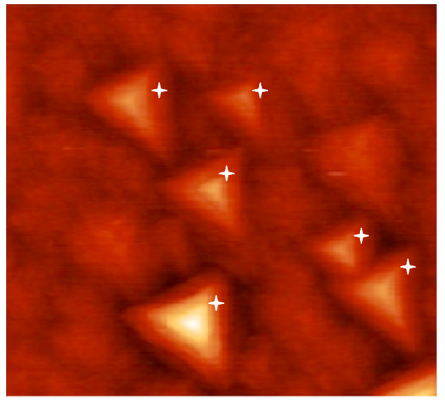
A typical AFM topographical image is presented in Fig. 1. We can clearly identify two families of pyramidal shaped structures with different size and aspect ratio (the ratio between vertical over lateral dimensions), which are present in all the grown samples.
We will refer to the smaller structures as “islands” and to the big ones as “hillocks”. The roughness (in terms of RMS) due to islands is quite small (0.2-1 nm on 8x8 m2 area) while the contribution given by hillocks can be huge (2 nm) and their minimization is one of the points on which our study is focused on.
It’s worth noting that all the results we obtained with Al0.30Ga0.70As epilayer are also valid for Al content lower than the .
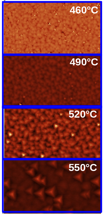
III.1 Temperature Series
We explored the 460-550∘C temperature range (see Table 1). At 460∘C, as reported in Fig. 2a, the growth of the Al0.30Ga0.70As epilayer is 3D like and the nucleated islands have the shape of rounded pyramids. Their average height is 2.5 nm with a base of 230 nm, and density of cm-2. The hillocks, instead, have a shape that resembles an irregular shamrock, that is a typical symptom of dendritic growth on surfaces with symmetryEinax et al. (2013). The hillocks average height is 10 nm with a base of 130 nm and density is cm-2. The overall roughness (RMS) on a 88 m2 area is around 1.17 nm, while the “background RMS” due to islands corrugation is around 1nm.
Raising the temperature up to 490∘C (Fig. 2b), the sample growth enters in a different regime. The islands and hillocks are regular triangular pyramids with net and definite sides. The average height, base and density of the island are 1.2 nm, 304 nm and cm-2 respectively; for hillocks we measured 4.4 nm, 225 nm and cm-2 respectively. The overall RMS on a 88 m2 area is decreased to 0.6 nm while the background RMS is 0.55 nm.
Increasing further the temperature (see Fig. 2c-d) the height and density of islands are reduce but their base increases. A different behavior can be seen for hillocks, for which height increases as well as the base (although the aspect ratio still shows a reduction). Hillock density does not change significantly within the temperature series. The overall RMS increases with the temperature due to the larger contribution from the hillocks to the value of 1.18 nm at 550∘C. The background RMS due to islands decreases to 0.4 nm.
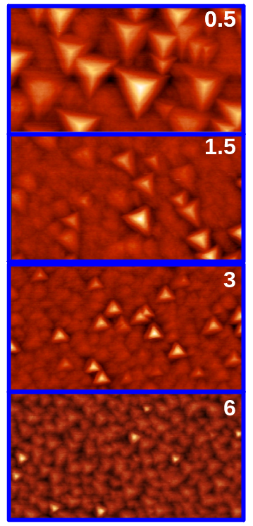
III.2 Grow rate series
We explored the atoms cm-2 s-1growth rate range (referred to group III adatoms) by changing simultaneously group III and group V flux but maintaining a constant V/III ratio (see Table 1). At a rate of atoms cm-2 s-1 big hillocks are observable with heights of more than 11 nm and base of 1.5 m (Fig. 3a). The areas free from hillocks are quite small (less than 2m2) and on the latter the islands are almost completely merged. Because of that, no reliable statistics on islands can be made, although a low background roughness can be inferred from the 0.38 nm background RMS (obtained excluding hillocks)
Increasing the growth rate (Figs. 3b-d), hillocks become smaller, keeping their density basically constant. Accordingly, the overall RMS decreases till the value of 0.57 nm at atoms cm-2 s-1. For what concerns islands, the increase of the growth rate results in larger density and aspect ratio. This leads to a rise of the background RMS.
III.3 V/III ratio series
The series spans 75-900 BEP V/III ratio range. At a ratio of 75, that is the one used for to realize the Temperature and Grow Rate series, the growth is 3D like with clearly distinguishable pyramidal hillocks. The overall RMS is around 0.57 nm and the background one is around 0.47 nm (Fig. 4a).
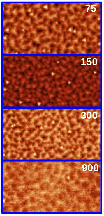
Decreasing the group III flux, in order to increase the V/III ratio till 300 (Fig.4c), only a small change is observed in island density, which only reduces by a factor two, from 6 to cm-2, when the V/III ratio increases from 75 to 300. Hillocks density is around cm-2 in the whole range. However, the height of the two pyramid families decrease proportionally to V/III passing from an average value of 1.4 nm to 0.7 nm for islands, and from a value of 4.5 nm to 2.26 nm for hillocks.
Going further, to a V/III ratio of 900 (Fig. 4d) the regime of growth passes from a 3D to a 2D like. The islands are practically one mono-layer high and the hillocks, if present, are completely indistinguishable from islands. The overall RMS (and obviously the background RMS) drops to a value of 0.2 nm. The dependence of the RMS on the relevant growth parameters in the three series is reported in Figs. 5.

IV Discussion
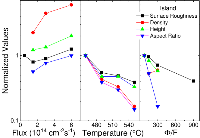
The description of the observed behavior of surface morphology, in terms of island RMS, density (), height and aspect ratio (height over base ratio) is reported in Fig. 6 . Some general trends can be identified. All the island relevant parameters tend to decrease with the increasing temperature and group-V () over group-III () ratio, while the trend is reversed in the case of dependence .
As a matter of fact, the variety of morphological observations in the three series resembles quite well what has been already reported in literature about the homoepitaxial growth on (111) oriented metals (Pt, Cu, Ag)Rosenfeld et al. (1997) with an fcc lattice. In these materials the growth dynamics is quite well understood and extensive models based on a kinetic growth framework have been developed Michely and Krug (2004). Within this scenario, it is natural to use the same basic concepts borrowed from the homoepitaxial growth of metals in the attempt of building an extended model for binary-alloy, like III-As materials, that could keep the same “predictive power” of the one made for metals.
The fundamental ingredient of (111) metal homoepitaxial models is the presence of a strong effective Ehrlich-Schwöbel (ES) barrier that, frustrating the escape of deposited adatoms from the top of a 2D nucleated island, drives the growth towards 3D. We suppose that the same phenomenon is playing a role in the observed behavior on GaAs. An estimation of the ES-barrier on Ga(Al)As (111)A is not available in the literature. However, a lower bound for the ES-barrier will follow directly from a–posteriori considerations after the construction of the model.
Before entering into the construction of the model it is worth to give a qualitative picture of what happens during the epitaxial growth, in order to fix some fundamental ideas and define the needed parameters.
In a layer-by-layer regime, after an “initial delay time”, the adatoms impinging on the substrate surface start to aggregate and to form small 2D islands. After the nucleation of 2D islands, depending on the surface coverage and on single island size, the atoms coming from the cells have a certain probability of direct impingement onto the top of the freshly formed 2D islands.
In this case, after a time called residence time, on which the adatom explores the island surface, three events can occur: 1)the adatom re-evaporate; 2) the adatom descends from the island top and eventually sticks on the step-edge or starts the nucleation of a new island; 3) the adatom meets other adatoms and starts to nucleate a new island on the top of the previous one. Being in a complete condensation regime we will completely discard re-evaporation processes. Depending on which of the two remaining events dominates, the growth will proceed 2D or 3D like.
Assuming the case where the adatom diffusion is quite efficient and therefore the diffusion length is larger than the average equivalent radius of the 2D islands (), the factor that can lead to multilayer nucleation is the ES-barrier. A large value of the ES-barrier, in fact, induces an increase of the residence time and an increase of the probability of adatoms encountering on the top of the island.
Within this kinetic framework three classes of parameters are important for the determination of the growth dynamics (see Michely and Krug (2004)):
-
•
the ones related to intralayer diffusion;
-
•
the ones related to ES-barrier;
-
•
the ones related to the growth parameters.
In the first class we find the diffusion length , the diffusion time and the diffusivity . These parameters are related one to each other by the formula , where the rate for a diffusion process, depending on the temperature and on the diffusion barrier , is given by the law , with is the attempt frequency.
In the second class we find the ES length and the ES time , where is the lattice parameter and, similar to what is seen for the diffusion process, is the rate of descending from step-edge regulated by the law , where is the sum of the and of the ES-barrier .
In the growth parameters class we have the temperature , the flux of Ga and the flux of As .
IV.1 Description of the model
It’s worth noting that the all growths were conducted in group III limited conditions (As overpressure). In these conditions, once the As pressure is effectively taken into account in the value of diffusivity, the growth rate is completely determined by the group III (Ga and/or Al) flux only. For these reasons, using the term “adatom” we will refer to group III adatoms only.
Moreover, similarly to what has been done for metalsMichely and Krug (2004), we will assume that in our growth conditions the growth dynamics is not dominated by intrinsic (extremely low diffusivity) or extrinsic (high growth rate) limitation in the adatoms diffusion path. These assumptions are not free from consequences and impose important bounds between the relevant time scales of our model.
In order to discard a diffusivity limited dynamics, we should impose that the time elapsed by the adatom on the island edge trying to overcome the ES barrier and be incorporated in the island edge is larger than the time needed to explore the island top surface : . This way the residence time , which is roughly the sum of the two contributions ( and ), satisfies the condition , that is diffusivity dynamics plays only a minor role in determining the residence time. This condition remains true till the multilayer nucleation takes place on the top of a layer (for the second layer is the base of the island, for the third is the second layer and so on) with radius , where is the critical radius for which :
| (1) |
To discard dynamics limited by high growth rates, we should impose that the average delay time between the arrival of two adatoms on the top of a 2D island of radius satisfy the relation . This relation also reflects on the island radius giving the relation with given by:
| (2) |
Borrowing from metalsMichely and Krug (2004) a value of on the order of Hz, from GaAs (001)Bietti et al. (2014) a value at C for of cm2s-1 and setting = cm-2s-1, , we get values for and of nm and nm respectively. Although these values are just indicative, because the used values of and for are just educated guesses of what happens on AlGaAs(111)A surfaces, they anyway show a sort of internal consistency of our model. In fact, in addition to being both in a ”reasonable” range for the phenomena we are considering, they are also of the same order of the average radius that can be infered from the AFM measurements. The formation of a nucleus on the second layer requires, first, that (at least) two atoms are present on the island simultaneously, and, second, that the two meet before one of them escapes from the island.
Under the assumption , the probability that an adatom, deposited at a time is present on top of a 2D island, at a time later than the arrival time of a second atom, can be approximated as follows Michely and Krug (2004):
| (3) | ||||
In the case of strong step edge barriers the two atoms will almost certainly meet, because their residence time is much larger than the encounter time, which can be roughly identified with the diffusion time . The probability for a freshly deposited atom to form a nucleus is therefore equal to the probability that another atom is present on the island at its deposition. Multiplying this probability for the average arrival rate on the island top , we get the rate
| (4) |
that two adatoms are present at the same time on top of an island. The rate is intuitively proportional to second layer nucleation rate, except in the special case for which the critical nucleus (two adatoms for nucleation). In this case in fact will be exactly equal to second layer nucleation rate and consequently Eq. (4) will return the value of the latter.
This rate changes very fast depending on island radius, passing for example (using the previously estimated values for and ) from Hz when nm, to a value of Hz at nm.
The dependence on growth parameters and in Eq. (4) is still hidden, and few more steps are needed to make this dependence explicit.
The dependence of the average radius on the growth parameters can be given by the formula:
| (5) |
where is constant, is the volume of group III elements, the value depends on the island shape, is the density of islands and is the coverage. In order to evaluate the dependence of on the growth parameter , and we extended Ref. Venables et al. (1984) results, by including the effects of As flux via its influence on the Ga diffusion length. This has been done by adding a power dependence to the island density of the form , with as the effect of As flux is to reduce the Ga diffusion Bietti et al. (2014) and hence to increase the island density.
| (6) |
where is a weak function of the coverage, being Ga adatom kinetics in the complete condensation regime Venables et al. (1984) (with depending on growth dimensionalityVenables et al. (1984)) and is the nucleation energy. Using this expression in Eq. (5) the following relation for the average radius can be deduced
| (7) |
where is a weak function of the coverage . Inserting Eq. (7) in Eq. (4) and using the definition of previously given, we can finally get
| (8) |
where is, also in this case, a weak function of the coverage. The island second layer nucleation rate depends on two adatom coexistence at the island top, thus gives a direct access to the dependence of surface roughness on the growth parameters. It is worth noting that being the exponent , for any value of , we get that , so that increases proportionally with the increasing of Ga flux . The exponent is always positive, being the effect of As flux to decrease group III adatom diffusion Horikoshi et al. (2007); Uehara et al. (2007)
IV.2 Discussion of the results
A fundamental ingredient for the discussion is the knowledge of the parameters involved in the model, namely the two exponents and , the activation energy , and the ES barrier energy . The a–priori knowledge of their values is precluded to us, being the growth dynamics too complex in the case of III-V compounds. However, by fitting the island density dependence on the growth conditions, we can obtain a direct measure of at least three of the four parameters involved, as explicitly depends on , and (see Eq. (6)). The obtained values are: , and from wich we can infer that . It is worth noting that, despite the large error bar, the value is in qualitative agreement with the expected exponent for the dependence on the Ga flux: . Inserting the parameters in Eq. (8) it is possible to derive some general rules regarding second layer nucleation in different growth conditions. A little more algebra must be performed when looking for the dependence on V/III ratio . In the case that the ratio is varied at constant we obtain while in the opposite case (constant ) .
-
1.
second layer nucleation increases with the increasing of Ga flux , being the exponent always positive in the complete condensation regime, so that 3D growth is favored by higher ;
-
2.
second layer nucleation decrease with the increasing of As flux , being a positive quantity, so that 3D growth is hindered by higher ;
-
3.
second layer nucleation is decreasing function of increasing V/III ratio, being the exponents and always negative, so that 3D growth is hindered by higher ;
-
4.
second layer nucleation decrease with the increasing of temperature , so that 3D growth is hindered by higher , if .
Following the considerations made at the end of the last sub-section, we can interpret the morphological observations as a function of the growth parameters by means of Eq. (8). Concentrating our attention on the islands, we clearly see that our model well describes the experimental results, being the surface roughness an increasing function of and a decreasing function of and (rules 1-3). In the temperature series (see Fig. 2) 3D growth is reduced for the islands by increasing the substrate temperature. This observation sets the ES energy value eV (see rule 4). The value of on GaAs(111)A is not available in the literature. We can have an estimate of it using theoretical calculations on GaAs(001) where eV. The additional step edge barrier related to the ES edge effect is then expected to be larger than one hundred meV.
However, when considering the actual overall surface roughness dependence on the growth conditions, we should pay attention to other factors that cannot be included in the ES-model that has brought us to Eq. (8), like extended defects and regime transitions.
A good starting point for such discussion is represented by the temperature series. Although the island population shows a reduction of the 3D growth with the increasing , and consequently a lower RMS at high temperatures, this is not what is observed on the surface overall. Hillock growth dynamics follows, in fact, a different behavior. The defect nature Horikoshi et al. (2007); Uehara et al. (2007) of hillocks tends to promote second layer nucleation and to increase their capture area proportionally to surface diffusion. This leads the morphological behavior of hillocks in the “opposite direction” with respect to what is expected for islands. However, this statement is not true for all the temperature range and adopting the strategy of decreasing the temperature in order to reduce the adatom diffusivity can be a bad choice. In fact, as previously reported, decreasing the temperature we enter may in a growth regime (dendritic regime), where diffusivity is very low, the step edge reorganization processes are hindered and the kinetic roughening dominates completely the final morphology.
This observation represents a crucial point. It demonstrates, in fact, that thinking on the transition from a 3D growth to a 2D like only as a diffusion limited process is too naive and in some way also incorrect.
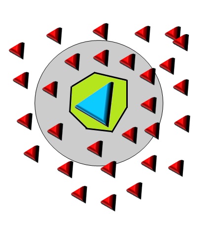
For what concerns the growth rate series, we can see again that, while islands follow the model prediction, that is an increase of the surface roughness with the increasing growth rate, the behavior of hillocks go exactly in the opposite direction (see Figures 5 and 6). The reason is the same discussed for the temperature series, that is a change of the capture area of the hillocks with the growth conditions. Although in this case the capture area of the hillocks is no more determined by the adatom diffusion. In fact, increasing the growth rate we are also increasing the island density, due to the increased probability of the formation of islands above the critical nucleus size Venables et al. (1984), thus reducing the inter-island distance well below the diffusion length. This increases the probability that an adatom is incorporated, during its diffusion, into a growing island, thus decreasing this way the adatom mean free path. This effectively reduces the adatom island capture area to values that can be much lower than the one set by diffusivity only. As shown in Figure 7, the effective mean free path is set by the average island-island distance, and this can be controlled by the island nucleation probability and thus, in turn, by the island density. This effect is clearly effecting strongly the hillock growth, as it is determined by the ability of the hillocks to accumulate material from the surroundings. The increase in group III flux, while favouring the second layer nucleation on the islands top, thus increasing island related roughness, it strongly limits the hillocks capture area, thus reducing hillock effects on the overall thickness.
As far as V/III ratio series is concerned, it is worth noting that during the growth of this series the As flux was kept constant, while the group III was decreased in order to increase the V/III ratio. We observe that the density of islands decreases when rising the V/III ratio but, contrary to what is seen in the the previous two series, the overall RMS decreases too. Looking at Eq. (8) we can see that the island behavior follows what is stated by the model, that is a decrease of second layer nucleation with increasing () ratio. What is different from the previous series is that in this case also the hillocks height decreases with rising the V/III ratio. The reason for this behavior can be ascribed to the fixed and high As flux. In fact, keeping the As flux constant at high values we are limiting the diffusivity of group III adatoms flux and thus, in turn, reducing the hillocks capture zone and hindering 3D growth on islands at the same time. Second layer nucleation is, in fact, proportional to . The exponent is in fact always negative, whichever is the critical nucleus size .
This is therefore fundamental for the control of the GaAs (111)A surface roughness to find a balance between the reduction of the effective mean free path, obtained both via diffusion length reduction and increase of island density, and the increase of the second layer nucleation, mostly controlled by group III adatom flux. This leads to the necessity to avoid too
IV.3 Quantum Well Optical Quality
The possibility to obtain extremely flat AlGaAs(111)A surfaces with RMS below nm opens to the fabrication of two dimensional quantum nanostructures with extremely narrow emission. For this purpose we fabricated a 5.5 nm thick, strain free GaA/Al0.3Ga0.7As quantum well. We expect, in fact, the excitonic linewidth and the AlGaAs/GaAs/AlGaAs interface RMS to be related by the equation Sanguinetti et al. (2008)
| (9) |
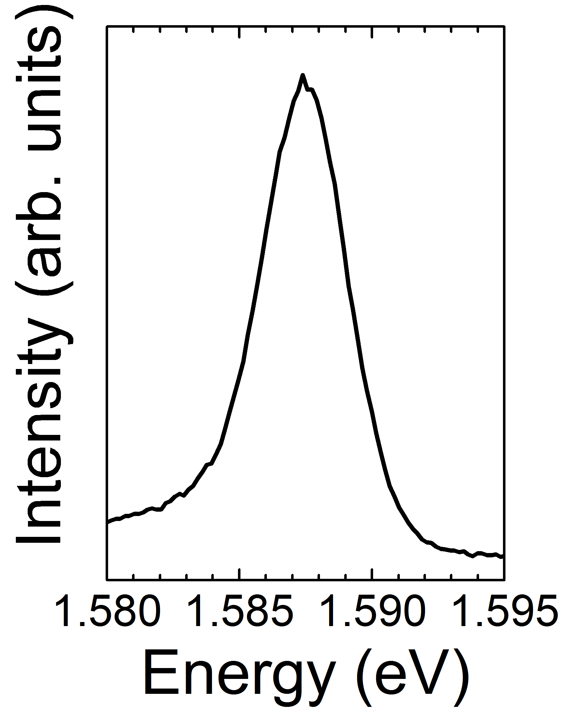
where is the quantum well thickness, is the energy of the interband excitonic transition in the quantum well, the energy gap of the quantum well material and the emission full width at half maximum. The emission spectrum of the fabricated quantum well is shown in Fig. 8. The well spectrum show with meV. Using the the experimental values , eV and in Eq. (9) we see that an emission broadening meV corresponds to a well width fluctuation of nm, in perfect agreement with the roughness value nm measured by AFM.
This is clear demonstration of how the high surface flatness control that can be reached by growth strategy and the procedures here presented strongly impact on the electronic properties of the quantum nanostructures realized on it. The quantum well in fact shows an extremely sharp emission of only 4.5 meV full width half maximum Cho et al. (2003).
V Conclusions
We presented a detailed study on how MBE growth parameters, namely temperature, growth rate and V/III ratio, impact on the growth dynamics of AlxGa1-xAs () (111)A surface. In particular we have identified and analyzed the factors that lead to huge overall roughness on this surface: i) the presence of defect induced hillocks; ii) the island 3D growth. The latter has been often overlooked in previous studies, thus preventing the achievement of a truly atomically flat surface Horikoshi et al. (2007); Uehara et al. (2007).
Our study has identified the Ehrlich-Schwöebel barrier as the leading factor on surface adatom dynamics. We then developed a novel theoretical model for the growth of III-V semiconductors in the presence of ES barriers. Within this framework we were able to interpret and control the island roughness. The hillocks related roughness is controlled by shrinking their capture area through an efficient mechanism of reduction of adatom mean free path via island density increase. This way we were able to drive the typical 3D growth of Ga(Al)As(111)A towards atomically flat surfaces ( nm RMS). Such low surface RMS was obtained at a substrate temperature of 520∘C, group III flux of 0.5 atoms s-1 cm-2 and V/III ratio of 900. These growth conditions are quite far from those typical of (001) surfaces and are dictated by the necessity of suppressing hillocks growth and promoting 2D growth of islands in the presence of a large Ehrlich-Schwöbel barrier. GaAs/Al0.30Ga0.70As quantum wells realized on such optimized surface show a record narrow emission linewidth of 4.5 meV.
The presented modeling of the growth dynamics on Ga(Al)As(111)A surfaces will permit to obtain quantum nanostructures with etremely sharp interfaces, thus reducing excitonic emission broading in QWs and carrier scattering at the interface in HMT fabricated on (111)A substrates, thus opening to the possibility of fabricating high efficiency HMT and optoelectronic devices.
References
References
- Miyata et al. (2011) N. Miyata, H. Ishii, Y. Urabe, T. Itatani, T. Yasuda, H. Yamada, N. Fukuhara, M. Hata, M. Deura, M. Sugiyama, M. Takenaka, and S. Takagi, Microelectron. Eng. 88, 3459 (2011).
- Xu et al. (2009) M. Xu, Y. Q. Wu, O. Koybasi, T. Shen, and P. D. Ye, Appl. Phys. Lett. 94, 212104 (2009).
- Hudait et al. (2013) M. K. Hudait, Y. Zhu, N. Jain, and J. L. Hunter, J. Vac. Sci. Technol. B 31, 011206 (2013).
- Li et al. (2005) H. Li, T. Mei, G. Karunasiri, W. J. Fan, D. H. Zhang, S. F. Yoon, and K. H. Yuan, J. Appl. Phys. 98, 054905 (2005).
- Zhang et al. (2013) D. Zhang, W. Lou, M. Miao, S.-c. Zhang, and K. Chang, Phys. Rev. Lett. 111, 156402 (2013).
- Hernandez-Minguez et al. (2012) A. Hernandez-Minguez, K. Biermann, R. Hey, and P. V. Santos, Phys. Rev. Lett. 109, 1 (2012).
- Balocchi et al. (2011) A. Balocchi, Q. H. Duong, P. Renucci, B. L. Liu, C. Fontaine, T. Amand, D. Lagarde, and X. Marie, Phys. Rev. Lett. 107, 1 (2011), arXiv:arXiv:1107.5642v1 .
- Weng and Wu (2013) M. Q. Weng and M. W. Wu, Phys. Rev. B 88, 1 (2013).
- Ye et al. (2012) H. Q. Ye, G. Wang, B. L. Liu, Z. W. Shi, W. X. Wang, C. Fontaine, A. Balocchi, T. Amand, D. Lagarde, P. Renucci, and X. Marie, Appl. Phys. Lett. 101, 032104 (2012).
- Zhao et al. (2014) C. Zhao, J. Li, Y. Yu, H. Ni, Z. Niu, and X. Zhang, Appl. Phys. Lett. 104, 052411 (2014).
- Mano et al. (2010) T. Mano, M. Abbarchi, T. Kuroda, B. McSkimming, A. Ohtake, K. Mitsuishi, and K. Sakoda, Appl. Phys. Express 3, 065203 (2010).
- Stock et al. (2010) E. Stock, T. Warming, I. Ostapenko, S. Rodt, A. Schliwa, J. A. Töfflinger, A. Lochmann, A. I. Toropov, S. a. Moshchenko, D. V. Dmitriev, V. a. Haisler, D. Bimberg, J. A. Töfflinger, A. Lochmann, A. I. Toropov, S. a. Moshchenko, D. V. Dmitriev, V. a. Haisler, D. Bimberg, J. A. Töfflinger, A. Lochmann, A. I. Toropov, S. a. Moshchenko, D. V. Dmitriev, V. a. Haisler, and D. Bimberg, Appl. Phys. Lett. 96, 093112 (2010).
- Huo et al. (2013) Y. H. Huo, a. Rastelli, and O. G. Schmidt, Appl. Phys. Lett. 102, 152105 (2013).
- Karlsson et al. (2010) K. F. Karlsson, M. A. Dupertuis, D. Y. Oberli, E. Pelucchi, A. Rudra, P. O. Holtz, and E. Kapon, Phys. Rev. B 81, 161307 (2010).
- Dupertuis et al. (2011) M. A. Dupertuis, K. F. Karlsson, D. Y. Oberli, E. Pelucchi, A. Rudra, P. O. Holtz, and E. Kapon, Phys. Rev. Lett. 107, 127403 (2011).
- Kuroda et al. (2013) T. Kuroda, T. Mano, N. Ha, H. Nakajima, H. Kumano, B. Urbaszek, M. Jo, M. Abbarchi, Y. Sakuma, K. Sakoda, I. Suemune, X. Marie, and T. Amand, Phys. Rev. B 88, 041306 (2013), arXiv:arXiv:1302.6389v1 .
- Singh and Bester (2010) R. Singh and G. Bester, J. Phys. Conf. Ser. 245, 012008 (2010).
- Uehara et al. (2007) T. Uehara, T. Iwai, I. Yoshiba, and Y. Horikoshi, Jpn. J. Appl. Phys. 46, 496 (2007).
- Horikoshi et al. (2007) Y. Horikoshi, T. Uehara, T. Iwai, and I. Yoshiba, Phys. Status Solidi 244, 2697 (2007).
- Johnson et al. (1994) M. D. Johnson, C. Orme, A. W. Hunt, D. Graff, J. Sudijono, L. M. Sander, and B. G. Orr, Phys. Rev. Lett. 72, 116 (1994).
- Michely and Krug (2004) T. Michely and J. Krug, Islands, Mounds and Atoms (Springer Verlag, Berlin, 2004).
- Einax et al. (2013) M. Einax, W. Dieterich, and P. Maass, Rev. Mod. Phys. 85, 921 (2013).
- Rosenfeld et al. (1997) G. Rosenfeld, B. Poelsema, and G. Comsa, Chem. Phys. Solid Surfaces 8, 66 (1997).
- Bietti et al. (2014) S. Bietti, C. Somaschini, L. Esposito, A. Fedorov, and S. Sanguinetti, J. Appl. Phys. 116, 114311 (2014).
- Venables et al. (1984) J. A. Venables, G. D. T. Spiller, and M. Hanbuenchen, Rep. Prog. Phys. 47, 399 (1984).
- Sanguinetti et al. (2008) S. Sanguinetti, M. Guzzi, and M. Gurioli, in Charact. Semicond. Heterostruct. Nanostructures, edited by C. Lamberti (Elsevier, Amsterdam, 2008) pp. 175–208.
- Cho et al. (2003) S. Cho, A. Sanz-Hervas, A. Majerfeld, and B. W. Kim, Phys. Rev. B 68, 035308 (2003).