Phonon-limited carrier mobility in monolayer Black Phosphorous
Abstract
We calculate an electron-phonon scattering and intrinsic transport properties of black phosphorus monolayer using tight-binding and Boltzmann treatments as a function of temperature, carrier density, and electric field. The low-field mobility shows weak dependence on density and, at room temperature, falls in the range of 300 - 1000 cm2/Vs in the armchair direction and 50 - 120 cm2/Vs in the zig-zag direction with an anisotropy due to the effective mass difference. At high fields, drift velocity is linear with field up to 1 - 2 V/m reaching values of cm/s in the armchair direction, unless self-heating effects are included.
I Introduction
Recently, black phosphorous emerged as a new two-dimensional (2D) material, which has attracted a great deal of attention due to its excellent transport and optical properties Xia et al. (2014a); Liu et al. (2015a); Ling et al. (2015); Perello et al. (2015); Xia et al. (2014b); Engel et al. (2014); Youngblood et al. (2015); Guo et al. (2016); Buscema et al. (2014); Li et al. (2014a); Chen et al. (2015); Liu et al. (2014); Koenig et al. (2014). Black phosphorous exhibits direct bandgap ranging from 0.3 eV to 1.8 eV for bulk and monolayer films respectively, filling the space between the gapless graphene and wide-gap transition metal dichalcogenides. High mobility at room temperature Perello et al. (2015); Xia et al. (2014b), strong coupling with light, and high anisotropy all contribute to huge potential in application of black phosphorous for infrared imaging Engel et al. (2014), detection Youngblood et al. (2015); Buscema et al. (2014); Guo et al. (2016), and electronic applications Li et al. (2014a); Koenig et al. (2014); Liu et al. (2014); Chen et al. (2015). However, little is known about the interplay of the acoustic and optical phonon scattering as a a function temperature, carrier density, and electric field.
Here we calculate the electron-phonon interactions and drift velocity in a monolayer black phosphorous, within a standard tight binding approach. Our results provide a detailed microscopic picture of phonon scattering. In particular, we find that two optical phonons with energies of around 400 cm-1 dominate scattering at room temperatures with acoustic phonon contribution being around 30%. The carrier density dependence of the low-field mobility is weak, such that mobilities at rooms temperature vary by a factor of three as carrier density varies by three orders of magnitude from 1011 cm-2 to 1014 cm-2. This is a consequence of a constant density of states in 2D.
II Theoretical Model
For the transport calculations, we use Fermi Golden rule to obtain the electron-phonon scattering rates. The model ingredients include: single-particle band structure fitted to GW calculations from Ref. Rudenko and Katsnelson (2014); valence force phonon model fitted to DFT calculations from Ref. Zhu and Tománek (2014); and electron-phonon coupling constants fitted to our DFT calculations shown in Appendix A.
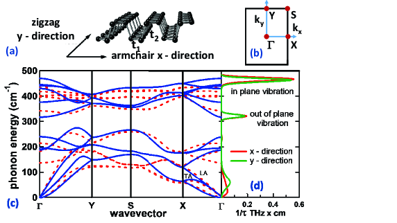
The single-particle band structure of black phosphorous monolayer can be obtained within the nearest-neighbor interactions in-plane eV and out-of-plane eV hopping integrals, respectively, as shown in Fig. 1a. The bandgap and effective masses in our model are:
| (1) |
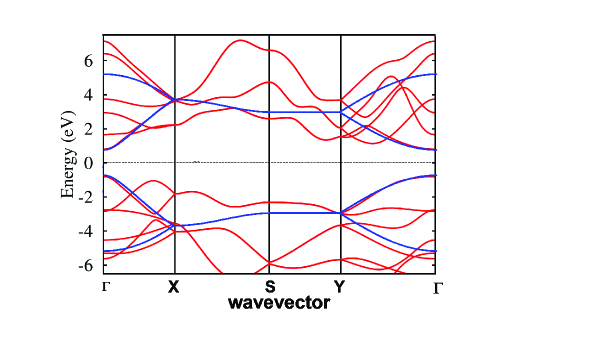
where is the electron mass and the lattice parameters Å and Å are along the armchair () and the zig-zag () directions, respectively. The bandgap is consistent with the experiment Li et al. (2017) and GW calculations Rudenko and Katsnelson (2014); Tran et al. (2014); Li et al. (2017) and effective masses with the density functional theory calculations Li et al. (2014b); Qiao et al. (2014); Peng et al. (2014). The overall bandstructure of our parametrization of the tight binding model agrees fairly well with that from GW calculations in Ref. Rudenko and Katsnelson (2014) near the top of the valence bands and bottom of the conduction bands, as shown in Fig. 2.
For the phonon model, we use a two parameter Keating-type model Keating (1966):
| (2) |
where is a distance variation between the neighbouring atoms and and is a variation of the angle made up by the three neighbouring atoms , and . Variables marked with superscript zero correspond to the equilibrium lattice structure Morita (1986); Liu et al. (2015a); Peng et al. (2014). The best fit to the phonon dispersion from the DFT calculations Zhu and Tománek (2014), shown in Fig. 1c, uses the bond stretching stiffness eV/Å2 and the bending stiffness eV.
The electron-phonon interaction is modelled by the Su-Schrieffer-Heeger (SSH) hamiltonian Su et al. (1979) with distance dependent hopping integrals and . Using our DFT calculations of the bandgap modulation as a function of an applied in-plane and out-of-plane strain to a black phosphorus monolayer as shown in Appendix A, we find e-ph coupling constants eV/Å and eV/Å. The Fourier transformed SSH Hamiltonian is
| (3) |
where is the e-ph coupling 111Here we neglect terms corresponding to the virtual electron-hole pair excitations across the bandgap., () denotes creation (annihilation) of an electron in the conduction band with index , is a phonon creation operator with wavevector and phonon band index . Previous studies of the intrinsic mobilities used the deformation potentials to describe acoustic phonon Qiao et al. (2014); Rudenko et al. (2016) and flexural phonon modes Rudenko et al. (2016) scattering. Inclusion of the optical phonon scattering Liao et al. (2015) predicted lower mobilities.
The low-field electron mobility can be calculated according to Appendix B:
| (4) | |||||
| (5) |
where labels direction of an electric field, is the electron-phonon scattering rate, is the equilibrium Fermi Dirac distribution at temperature and Fermi energy , is the band velocity at wavevector index , which absorbs both wavevector direction and electron band index. The hole mobility is identical, due to the electron-hole symmetry in our model.
III Results
In Fig. 1d we show relative contributions of different phonons to the scattering rate in Eq. (4), weighted average by a distribution for cm-2 and K. The weighted average of the scattering times in and directions are very similar, as shown in Fig. 1d. The areas under both curves in Fig. 1d correspond to the scattering times fs and fs, which would suggest Drude mobilities to be cm2/Vs and cm2/Vs, respectively. This is consistent with the full calculations of the low-field mobilities according to Eq. (5) cm2/Vs and cm2/Vs.
For a high field , drift velocity can be obtained from the numerical solution of the Boltzmann transport equation 222The Brillouin zone mesh of 1000 500 and energy cut off 0.5 eV above the bottom of the conduction band were employed to transform Boltzmann transport equation to a matrix form and to solve it iteratively. for the distribution function :
| (6) |
We find that mobility from the Boltzmann transport equation solution Eq. (6) differs by 5%-10% from the mobility calculated from Eq. (5).
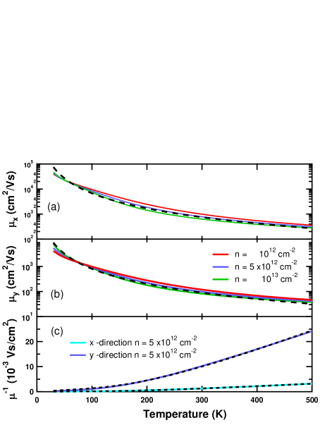
Fig. 3 shows temperature dependence of the low-field mobility for different concentrations. As expected, phonon-limited mobility decreases with temperature but exhibits several peculiarities. In the armchair direction, the room temperature mobility values are not as large as in graphene, but higher than that in silicon and other currently employed materials confirming high potential of black phosphorus in electronics and optoelectronics. In the zig-zag direction, mobility values are about eight times lower due to the differences in the effective masses.
The overall temperature dependence appears as a power law in Fig. 3a and 3b. However, a more detailed analysis based on the scattering rate from Fig. 1d suggests contributions from both acoustic and optical phonons, which can be accounted for by an empirical expression as motivated by the Matthiessen rule Ashcroft and Mermin (1976):
| (7) |
where K and three fitting parameters are acoustic phonon limited mobility at , optical phonon limited mobility at , and optical phonon energy . Using cm2/Vs, cm2/Vs for direction and cm2/Vs, cm2/Vs for direction, and phonon energy of cm-1 (or 56 meV), Eq. (7) reproduces very well calculated mobility temperature dependence, as shown in Fig. 3c.
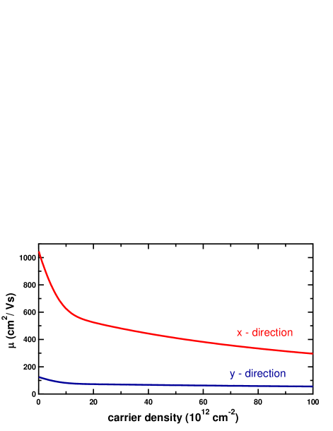
The mobility variation with carrier density at room temperature is weak, as shown in Fig. 4. We attribute this behaviour to the constant density of states in 2D and dominant contribution of the optical phonon scattering at room temperature. At carrier density of about cm-2, the Fermi level coincides with the optical phonon energy. This causes suppression of the optical phonon emission due to the lack of the final density of states. As a result, mobility increases by roughly a factor of two in the limit of low carrier density. Note, that the carrier density dependence exhibits different behaviour at low temperatures below K, where acoustic phonon contribution dominates, such that mobility slightly increases as the carrier density increases.
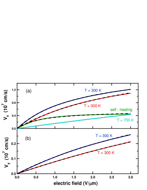
For electronic applications velocity saturation is important. At high electric fields, drift velocity for both directions is shown in Fig. 5a and 5b. We find that for a constant phonon temperature, i.e. isothermal calculations, there is a weak sign of the velocity saturation due to the optical phonon scattering at the experimentally accessible field strengths. This is opposite to the case of graphene, where high energy optical phonon scattering is much stronger then the acoustic phonon scattering which leads to the velocity saturation Meric et al. (2008); Perebeinos and Avouris (2010). Dashed curves in Fig. 5 are fits to the velocity saturation expression:
| (8) |
where is the low-field mobility and is the saturation velocity. A reference field , at which velocity shows saturation, can be defined as . For the armchair direction, we find V/m and 3.3 V/m for cm-2 and cm-2, correspondingly, and V/m and 14 V/m for the zig-zag direction, respectively. Such high value sof imply an absence of the velocity saturation, except for cm-2 case in the armchair direction, when cm/s from the fit to Eq. (8).
Nevertheless, the Joule losses lead to the temperature rise as , where K is an ambient temperature, is the electric current, and is the thermal conductance. The upper bound for , for a monolayer device on an insulating substrate, corresponds to the zero contact thermal resistance between the black phosphorus and the substrate. Such that is determined by the thermal conductivity and thickness of an insulating substrate. For example, for an oxide thickness with nm of SiO2 substrate with thermal conductivity of W/(mK) Ref. Shackelford and Alexander (2000), a maximum value of kW/(K cm2) is expected. Calculations with the self-heating effects included lead to the velocity saturation at much smaller field of V/m and saturated velocity of cm/s, as shown in Fig. 5a. We also show in Fig. 5a an isothermal calculations at the burning temperature of black phosphorous few tens of nm thick sample Engel et al. (2014). However, in the high bias experiments on few tens of nm samples in Ref. Engel et al. (2014) and Ahmed et al. current was almost linear up to the break down voltage. This may imply an important role of the electron-hole pair excitation across the small bandgap of eV in multilayers at high temperatures and large electric fields. Such that increased would overwhelm a reduction of due to the saturation.
IV Conclusions
In conclusion, using a tight-binding model with parameters benchmarked by the DFT calculations, we have predicted phonon limited transport of black phosphorous as a function of temperature, carrier density, and electric field. The low-field mobility is highly anisotropic with values along the armchair direction about eight times higher than that of the zig-zag direction. This difference stems from the high ratio of the effective masses and almost isotropic scattering rate. At room temperatures, optical phonons dominate the scattering leading to decreasing mobilities with increasing carrier densities. While transport data on monolayers are scare for a direct comparison, the available low bias measurements on black phosphorous multilayer samples are consistent with our predictions. We hope our work would stimulate further experiments on monolayer samples, which requires inert gas environments to prevent oxidation Koenig et al. (2014); Favron et al. (2015); Edmonds et al. (2015); Liu et al. (2015b).
Appendix A
DFT derived parameters for the electron-phonon scattering
Using WIEN2k density functional theory (DFT) code Blaha et al. (2001) within the PBE functional Perdew et al. (1996), for a monolayer black phosphorous we obtained the internal parameter and the equilibrium lattice constants of Å and Å along the armchair () and the zig-zag () directions, respectively. The layer separation in the direction was set at 1.5 inter layer distance, i.e. Å. (For the bulk black phosphorus we obtain values and Å.) The bandgap of 0.9 eV for a monolayer black phosphorus is consistent with the previous theoretical reports Liu et al. (2014); Qiao et al. (2014); Peng et al. (2014); Li et al. (2014b); Tran et al. (2014).
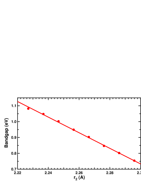
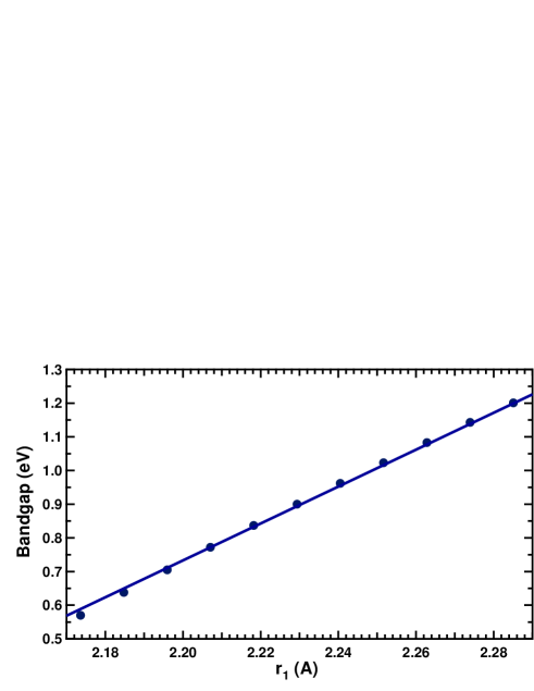
As we apply an out-of-plane strain in (001) direction, the out-of-plane bondlength increases, while the in-plane bondlength is constant. As a result, the bandgap reduces, as shown in Fig. (6). For the in-plane strain along the (110) direction, the in-plane bondangle is constant and the bandgap increases, as shown in Fig. (7). Using a relationship between the bandgap and the hoping integrals from Eq. (1) in the main text, i.e. , we can obtain:
| (9) | |||||
| (10) |
where is due to the geometrical factor, i.e. the out-of-plane P-P bond is not perpendicular to the plane. The best fits of the bandgap change with an applied strain to Eq. (9) and (10) result in the values of eV/Å and eV/Å.
Appendix B
Relaxation time approximation for an anisotropic material
We are looking for a solution of the Boltzmann transport equation (BTE) for a carrier distribution function in an external electric field, without loss of generality, along the direction:
| (11) |
where is a collision integral, is an electron-phonon scattering rate, and is carrier momentum.
The distribution function can be written in the form
| (12) |
where is the equilibrium Fermi Dirac distribution. We assume that is small and linear in . In the collision integral, the zeroth order terms in sum to zero and the second order terms in field strength are discarded, such that:
Using the detailed balance relationship , Eq. (B) transforms to
| (13) |
Using an ansatz for the distribution function
| (14) |
the collision integral takes the form:
| (15) |
where is the band velocity. The left hand side of the BTE, which is linear in , is given by:
| (16) |
such that the BTE equation reduces to:
| (17) |
References
- Xia et al. (2014a) F. Xia, H. Wang, D. Xiao, M. Dubey, and A. Ramasubramaniam, Nat. Photon 8, 899 (2014a).
- Liu et al. (2015a) H. Liu, Y. Du, Y. Deng, and P. D. Ye, Chem. Soc. Rev. 44, 2732 (2015a).
- Ling et al. (2015) X. Ling, H. Wang, S. Huang, F. Xia, and M. S. Dresselhaus, PNAS 112, 4523 (2015).
- Perello et al. (2015) D. J. Perello, S. H. Chae, S. Song, and Y. H. Lee, Nat. Comm. 6, 7809 (2015).
- Xia et al. (2014b) F. Xia, H. Wang, and Y. Jia, Nat. Comm. 5, 4458 (2014b).
- Engel et al. (2014) M. Engel, M. Steiner, and P. Avouris, Nano Lett. 14, 6414 (2014).
- Youngblood et al. (2015) N. Youngblood, C. Chen, S. J. Koester, and M. Li, Nat. Phot. 9, 247 (2015).
- Guo et al. (2016) Q. Guo, A. Pospischil, M. Bhuiyan, H. Jiang, H. Tian, D. Farmer, B. Deng, C. Li, S.-J. Han, H. Wang, et al., Nano Lett. 16, 4648 (2016).
- Buscema et al. (2014) M. Buscema, D. J. Groenendijk, S. I. Blanter, G. A. Steele, H. S. J. van der Zant, and A. Castellanos-Gomez, Nano Lett. 14, 3347 (2014).
- Li et al. (2014a) L. Li, Y. Yu, G. J. Ye, Q. Ge, X. Ou, H. Wu, D. Feng, X. H. Chen, and Y. Zhang, Nat. Nano 9, 372 (2014a).
- Chen et al. (2015) X. Chen, Y. Wu, Z. Wu, Y. Han, S. Xu, L. Wang, W. Ye, T. Han, Y. He, Y. Cai, et al., Nat. Comm. 6, 7315 (2015).
- Liu et al. (2014) H. Liu, A. T. Neal, Z. Zhu, Z. Luo, X. Xu, D. Tománek, and P. D. Ye, ACS Nano 8, 4033 (2014).
- Koenig et al. (2014) S. P. Koenig, R. A. Doganov, H. Schmidt, A. H. Castro Neto, and B. Özyilmaz, Appl. Phys. Lett. 104, 103106 (2014).
- Rudenko and Katsnelson (2014) A. N. Rudenko and M. I. Katsnelson, Phys. Rev. B 89, 201408 (2014), URL http://link.aps.org/doi/10.1103/PhysRevB.89.201408.
- Zhu and Tománek (2014) Z. Zhu and D. Tománek, Phys. Rev. Lett. 112, 176802 (2014), URL http://link.aps.org/doi/10.1103/PhysRevLett.112.176802.
- Li et al. (2017) L. Li, J. Kim, C. Jin, G. J. Ye, D. Y. Qiu, F. H. da Jornada, Z. Shi, L. Chen, Z. Zhang, F. Yang, et al., Nat. Nano 12, 21 (2017).
- Tran et al. (2014) V. Tran, R. Soklaski, Y. Liang, and L. Yang, Phys. Rev. B 89, 235319 (2014).
- Li et al. (2014b) Y. Li, S. Yang, and J. Li, J. Phys. Chem. C 118, 23970 (2014b).
- Qiao et al. (2014) J. Qiao, X. Kong, Z.-X. Hu, F. Yang, and W. Ji, Nat. Comm. 5, 4475 (2014).
- Peng et al. (2014) X. Peng, Q. Wei, and A. Copple, Phys. Rev. B 90, 085402 (2014).
- Keating (1966) P. N. Keating, Phys. Rev. 145, 637 (1966), URL http://link.aps.org/doi/10.1103/PhysRev.145.637.
- Morita (1986) A. Morita, Applied Physics A 39, 227 (1986), ISSN 1432-0630, URL http://dx.doi.org/10.1007/BF00617267.
- Su et al. (1979) W. P. Su, J. R. Schrieffer, and A. J. Heeger, Phys. Rev. Lett. 42, 1698 (1979), URL http://link.aps.org/doi/10.1103/PhysRevLett.42.1698.
- Rudenko et al. (2016) A. N. Rudenko, S. Brener, and M. I. Katsnelson, Phys. Rev. Lett. 116, 246401 (2016).
- Liao et al. (2015) B. Liao, J. Zhou, B. Qiu, M. S. Dresselhaus, and G. Chen, Phys. Rev. B 91, 235419 (2015).
- Ashcroft and Mermin (1976) N. Ashcroft and N. Mermin, Solid State Physics (Saunders College, Philadelphia, 1976).
- Meric et al. (2008) I. Meric, M. Y. Han, A. F. Young, B. Ozyilmaz, P. Kim, and K. L. Shepard, Nat Nano 3, 654 (2008), ISSN 1748-3387, URL http://dx.doi.org/10.1038/nnano.2008.268.
- Perebeinos and Avouris (2010) V. Perebeinos and P. Avouris, Phys. Rev. B 81, 195442 (2010).
- Shackelford and Alexander (2000) J. Shackelford and W. Alexander, CRC Materials Science and Engineering Handbook, Third Edition (CRC Press, 2000), ISBN 9781420038408, URL https://books.google.ru/books?id=gSOxul7qnZAC.
- (30) F. Ahmed, Y. D. Kim, M. S. Choi, X. Liu, D. Qu, Z. Yang, J. Hu, I. P. Herman, J. Hone, and W. J. Yoo, arXiv:1610.09951 (????).
- Favron et al. (2015) A. Favron, E. Gaufres, F. Fossard, A.-L. Phaneuf-L’Heureux, N. Y.-W. Tang, P. L. Levesque, A. Loiseau, R. Leonelli, S. Francoeur, and R. Martel, Nat. Mater. 14, 826 (2015).
- Edmonds et al. (2015) M. T. Edmonds, A. Tadich, A. Carvalho, A. Ziletti, K. M. O’Donnell, S. P. Koenig, D. F. Coker, B. Özyilmaz, A. H. C. Neto, and M. S. Fuhrer, ACS Appl. Mater. & Interfaces 7, 14557 (2015).
- Liu et al. (2015b) H. Liu, Y. Du, Y. Deng, and P. D. Ye, Chem. Soc. Rev. 44 (2015b).
- Blaha et al. (2001) P. Blaha, K. Schwarz, G. K. H. Madsen, D. Kvasnicka, and J. Luitz, WIEN2k, An Augmented Plane Wave+Local Orbitals Program for Calculating Crystal Properties, vol. 1 (Technische Universität Wien, Austria, 2001).
- Perdew et al. (1996) J. P. Perdew, K. Burke, and M. Ernzerhof, Phys. Rev. Lett. 77, 3865 (1996).