Photodoping-driven crossover in low-frequency noise in MoS2 transistors
Abstract
Transition metal dichalcogenide field-effect transistors (FETs) have been actively explored for low-power electronics, light detection, and sensing. Albeit promising, their performance is strongly limited by low-frequency noise (LFN). Here, we report on the study of LFN in MoS2 FETs on SiO2 substrates in ambient conditions using photodoping. Using this external excitation source allows us to access different non-equilibrium steady states and cross over different noise regimes. We observe a dependence of the noise power spectrum with the transient decay time window, approaching -type when the system is closer to equilibrium, and identify a dependence of the LFN with channel thickness. Monolayer/bilayer devices exhibit random telegraph noise for insulating regimes and -type Hooge mobility fluctuations (HMF) for conductive regimes. Thicker devices exhibit mainly -type carrier number fluctuations (CNF). In the latter, we observe a photodoping-induced change from a near parabolic to a near linear dependence of the inverse noise amplitude above the threshold gate voltage. This change indicates a crossover in the LFN mechanism from CNF to HMF. We demonstrate that the study of conductance and noise under photodoping is an effective tool to identify dominating carrier noise mechanisms in few-atomic-layer FETs for a wide range of doping regimes.
pacs:
72.70.+m Noise processes and phenomena; 72.80.Vp Electronic transport in graphene; 73.50.Pz Photoconduction and photovoltaic effectsI Introduction
Collective wavelike fluctuations are ubiquitous and inherent to two-dimensional (2D) van der Waals (vdW) semiconductors, being responsible for nontrivial modifications of noncovalent interactions at the nanoscale Ambrosetti2016 . In few-layer-thick 2D vdW electrical devices, the high surface-to-volume ratio and ultimate thinness of the channel make conduction electrons particularly vulnerable to traps, ionized impurities, and changes in the scattering cross-section. These fluctuations can manifest as low-frequency noise (LFN) with power spectrum closely following an inverse dependence with frequency , , where is a characteristic exponent. Although LFN dominates the power spectrum at low frequency, it is the main contributor to the phase noise of sensors and high-frequency operating systems due to its upconversion to high frequenciesBalandin2013 . For these reasons, LFN has emerged as a key limiting factor in the performance of 2D vdW-based devices, particularly under low doping regimes Sangwan2013 ; Renteria2014 ; Kwon2014 ; Cho2015 . It is thus crucial to understand the processes responsible for the fluctuation of the electrical current in such devices for future applications.
The unique electrical and optical properties of ultrathin films of transition metal dichalcogenides (TMDs) have been intensively explored in few-atomic-layer field-effect transistors (FETs) Radisavljevic2015 ; Sarkar2015 . MoS2 FETs in particular have been actively investigated for low-power electronics Radisavljevic2015 ; Wang2012 ; Kim2012 , light detection, photocurrent generation Furchi2014 ; Memaran2015 ; Buscema2015 , and sensing Perkins2013 ; Lin2015 .
In MoS2 FETs, the presence of trapping - de-trapping processes at the channel to insulator and vacuum interfaces has been demonstrated to drive bi-exponential current relaxationLate2012 , time-dependent contributions to the electron transport characteristicsGuo2015 , and to differences in the carrier density. These processes contribute to the slow relaxation of the photoconductivity in MoS2Wu2015 . In recent years, noise in mono-to-multilayer TMD FETs has been mainly described by carrier number fluctuations, (CNF)Joo2016 ; Ko2016 ; Das2015 ; Lin2015 ; Sharma2014 ; Ghatak2014 ; Xie2014 ; Renteria2014 ; Kwon2014 ; Na2014 ; Sharma2015 ; Rumyantsev2015 , with some exceptional cases reporting phenomenological Hooge mobility fluctuations, (HMF)Sangwan2013 ; Na2014 , where noise is interpreted in terms of the fluctuation of the free path length of the charge carriers Hooge1969 . This percolative nature of the electron conduction has been shown to be a dominant noise mechanism in multilayer WSe2 FETs Cho2015 ; Paul2016 . Although CNF is seen as the dominant LFN mechanism in MoS2, there is no clear explanation to the microscopic physical mechanisms behind noise in the cases where HMF has been observed. It is therefore worth investigating photodoping as an external stimulus to access different low-frequency noise regimes in a set of TMD-FETs with different thicknesses.
Here we present a study of electron transport and photoconductivity in monolayer to bulk MoS2 FETs to address three important questions: (i) how transient decays affect LFN in back-gated MoS2 FETs, (ii) whether photodoping, by modulating the charge carrier density, can change the LFN mechanisms, and (iii) if LFN mechanisms in MoS2 FETs undergo a significant change with incremental channel layer number. Furthermore, by providing an additional route to identify the physical mechanisms behind LFN in TMD FETs we pave the road to the development of alternative approaches to optimize TMD-based photodetectors and transistors.
II Experimental details
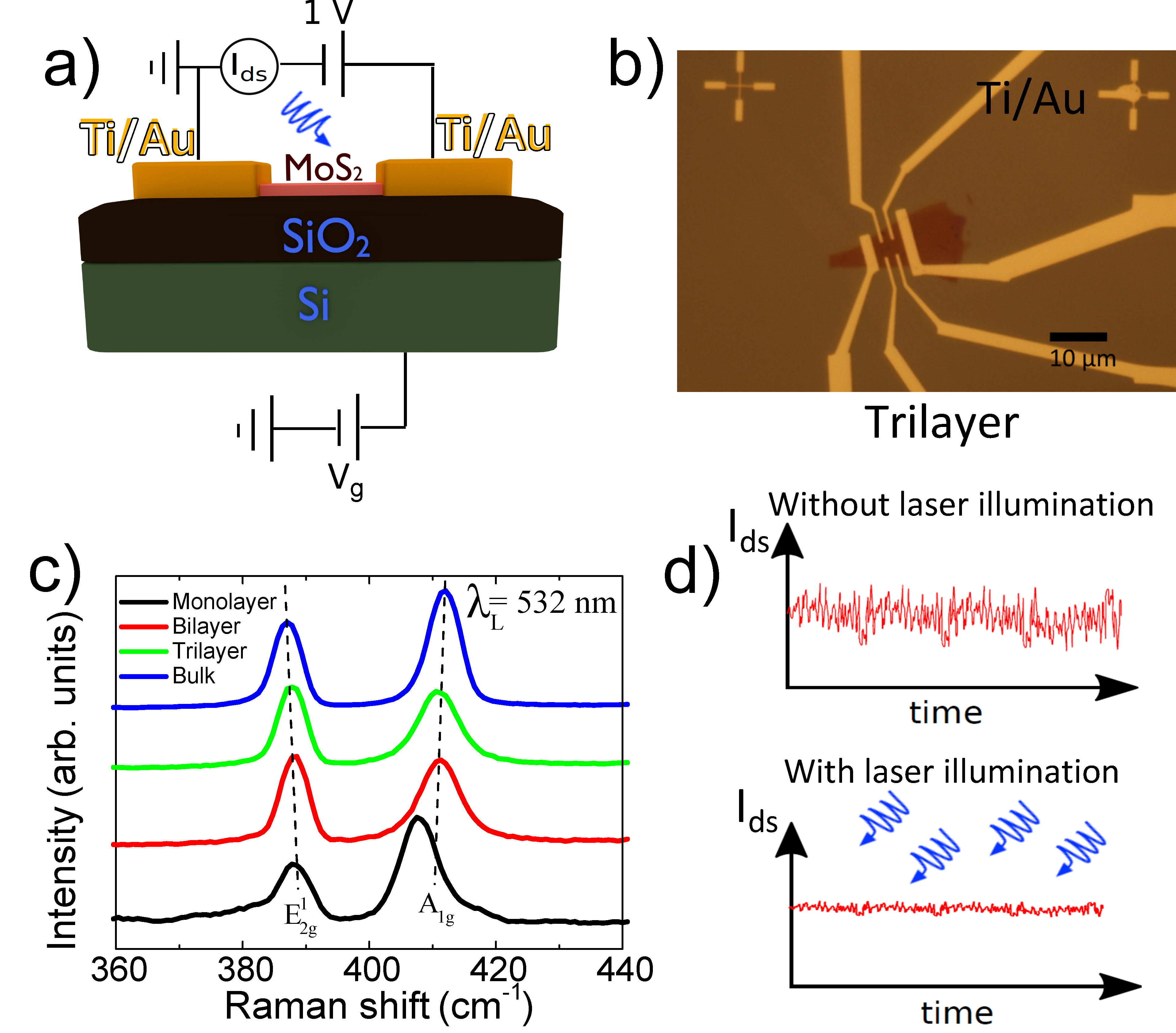
We studied four MoS2 FET devices with monolayer, bilayer, trilayer and bulk-like MoS2 channels, henceforth identified as device I, II, III and IV, respectively. The sample preparation was carried out using high-purity bulk MoS2 crystals acquired from a commercially available supplier (SPI Supplies). The MoS2 FETs were fabricated on n+-doped silicon dies with thermally grown 250-nm-thick SiO2. The substrates were cleaned and sonicated in acetone, isopropanol, and deionized water and dried on a hotplate at 195 ∘C. Following an all-dry viscoelastic stamping deterministic transfer procedure Castellanos2014 using polydimethylsiloxane (PDMS), MoS2 flakes with different number of atomic layers were optically identified and selectively transferred onto the SiO2 substrates. Standard electron-beam lithography using a double layer of poly methyl-methacrylate (PMMA, 495/950 MDa) was employed to pattern Ti(5 nm)/Au(35 nm) metal contacts. The metallization was done in an ultrahigh vacuum deposition system at a base pressure of mbar, using electron-beam evaporation to deposit Ti and Au. The lift-off was performed in acetone. Figure 1a) shows the sketch of the FET electrical configuration, with MoS2 channel, SiO2(250 nm) dielectric, Si backgate, and Ti(5 nm)/Au(35 nm) contacts. Figure 1b) shows a microscopic picture of device III.
The thickness of the MoS2 flakes was determined using Raman spectroscopy with a 532 nm laser line at room temperature (see Figure 1c). The difference between the frequency of the Raman and peaks, , can be used as a reliable indicator of the number of layers of the flake Li2012 . The frequencies of the peaks were determined using a double Lorentzian least square best fit. The obtained ) of 20.2, 22.8, 23.2, 24.9 cm-1 are in agreement with the expected values for monolayers, bilayers, trilayers and bulk-like, respectively. The lateral dimensions (length and width ) of device I were m and m; device II, m and m; device III, m and m; device IV, m and m.
Due to the relatively high resistance of the MoS2 FETs, both current and current noise were measured with a Keithley 6485 picoammeter. A home-made battery designed for ultra-low noise at a bias of 1 V powered the voltage applied between the drain and the source contacts, while a gate voltage up to 80 V was applied between the substrate and the drain using a Keithley 228A voltage source. In the set of measurements performed during this study, the amplifier noise and Johnson noise were orders of magnitude below the detected noise-levels, which allows us to disregard spurious origins for the observed signals.
The current intensity time series were measured at every fixed gate during 180 s with resolution of 67 ms. The FETs were illuminated with a TOPTICA-iBeam Smart diode laser with wavelength of 487 nm and with up to 1mW of nominal output power. The maximum effective light surface density was estimated to be substantially below 1 W/m2. The laser spot of about tens of m in diameter covered the whole surface of the MoS2 channel. All the measurements were performed at room temperature and in ambient conditions. LFN experiments were carried out by studying the current relaxation time series after steeply sweeping up the gate voltage by 2 V under two different conditions: (i) dark conditions, where no laser illumination was applied, and (ii) in the presence of laser illumination. Figure 1d) shows schematically how the normalized current noise varies under photodoping.
III Results and discussion
III.1 Electron transport with and without photodoping
In the body of the manuscript, we mainly concentrate on the results obtained for devices II and III, between which a significant change in the LFN under photodoping has been observed. Some relevant complementary results for devices I and IV are provided in the supplemental materials Supplemental materials .
We start by evaluating the DC transport with and without illumination to establish a foot-ground for the LFN studies. Figures 2a) and 2b) show the gate dependence of the drain-source current (transfer characteristics) with and without laser illumination. The non-illuminated FETs exhibit n-type behavior with ON/OFF ratios of the order of . In agreement with previous reports Late2012 ; Fontana2013 , the transfer characteristics of devices II and III reveals hysteretic behavior due to current relaxation. Qualitatively similar effects are shown Supplemental materials in Supplemental Figure 1S for devices I and IV. With laser illumination the current output of the transistor OFF state greatly increases from to A, while the current output at the ON state increases by a factor of two. In both cases the hysteretic behavior slightly increases, in line with previous studiesLate2012 .
Devices II and III exhibit maximum field-effect mobilities of 9 and 14 cm2/Vs respectively. The field-effect mobility of devices II and III are calculated from the expression = , where is the terminal transconductance (), and the gate capacitance per unit area, estimated to be 1.3810-4F/m2 for a 250-nm-thick SiO2 dielectric, using a parallel plate model. Ti/Au contacts to the MoS2 channel provide low Schottky barriers of 0.05 eV Allain2015 , which at room temperature result in ohmic-like output characteristics Supplemental materials (see supplemental Figure 2S).
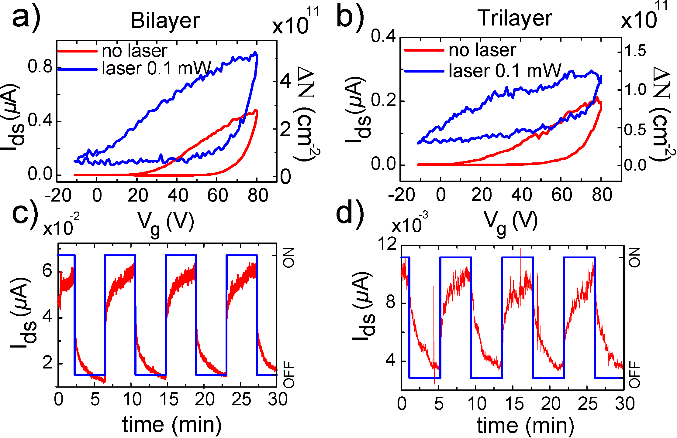
Figures 2c) and 2d) show the drain-source photocurrent generated by a laser pulse of period T = 500 s at zero gate voltage for devices II and III, respectively, under an applied drain-source bias, of 1 V. Exponential decay time constants of about 180 s are observed before reaching the equilibrium state, both for the ON and OFF states of the laser illumination. Similar curves for devices I and IV are shown Supplemental materials in Supplemental Figures 3Sa) and 3Sb). The normalized variation of the pulsed photocurrent as a function of the MoS2 channel thickness Supplemental materials (Supplemental Figures 3Sc) points out at a difference between devices with increasing number of layers, with maximum photocurrent response at 2 or 3 layers.
We estimate the additional photoexcited carrier density, , generated under illumination using a simplified relation between conductance, mobility, and carrier concentration, given by , with being the change in surface conductance, and hole and electron mobilities, and the change in hole and electron concentrations. Being n-doped, we assume the presence of one type of carriers only (electrons) and that for the minimum applied laser power (0.1 mW) the carrier concentration change is larger than the change in the Hall mobilityBritton2013 . Figure 2a) and b) show the change in carrier density between dark and illuminated states for device II and III.
III.2 Low frequency noise without photodoping
We now turn to investigate how the LFN parameters change along the current relaxation. For this, we used the determined exponential decay time constant of about 180 s. Photocurrent relaxation of similar time scales has been reported for MoS2 FETs Wu2015 , being attributed to the presence of random potentials in the device due to defects. For the noise analysis, we divided the current time series (both in dark condition and under illumination) in three periods, , each lasting for about 60 . For each of those intervals, the noise power spectrum of the current has been analyzed separately by using the Hooge relation Sangwan2013 ; Hooge1969 , , where is the square of the module of the fast Fourier transform of the current time series expressed as a function of the frequency , the source-drain current under equilibrium, and and characteristic Hooge parameters obtained from fits in the frequency range. When is close to one (i.e. roughly between 0.7 and 1.5) the noise is usually called noise Hooge1969 . The strong dependence of the channel resistivity with gate voltage (with a change up to 6 orders of magnitude between the ON and OFF states), requires that we fix the applied Vds and record continuously flowing through the device for consecutively increasing gate voltage steps of 2 V, with current fluctuations recorded for 180 s. Supplemental Figure 2S shows Supplemental materials that the devices are close to the Ohmic regime for the full range of gate voltages explored in this work, where is proportional to .
Figure 3a) exhibits the current time series dependence of device III under dark conditions after a steep sweep of by 2 V, and 3b) the corresponding gate dependence for the extracted parameter at P1, P2, P3. At the P3 interval, the relaxation effects are found to be negligible, and indicate that the system is close to equilibrium. Evaluating as the device operation approaches equilibrium (from P1 to P3), the exponent decreases from above 1.5 to closer to 1 (see Figure 3b), without exhibiting a significant gate dependence. The larger values in the presence of time dependent relaxation were also observed in off-equilibrium magnetic tunnel junctions near the switching to the antiparallel state Guerrero2002 . This dependence of the LFN with the period of the current time series was observed in all samples. In order to address possible concerns about spectral leakage along relaxation, we analyzed the LFN data only for the periods closest to equilibrium (P3).
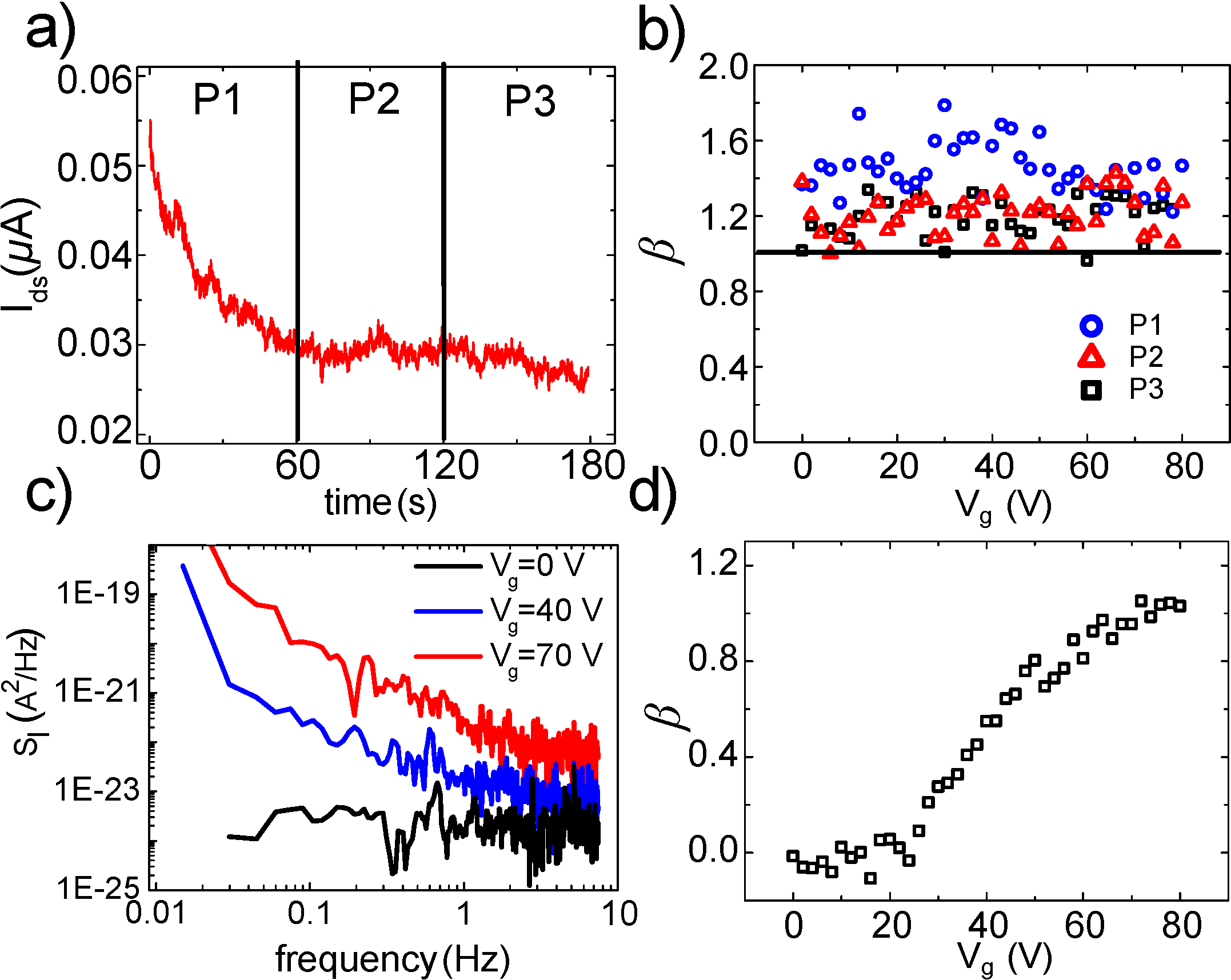
Focusing henceforth on the current time series period P3, device II exhibits a clear dependence of the with gate voltage. Figure 3c) shows the noise power spectrum under dark conditions at = 0, 40, and 70 V for device II. Plotting in log-scale allows us to clearly identify a power dependence with frequency with Hooge parameter increasing for higher gate voltages. Figure 3d) summarizes the gate dependence of for device II. For 20 V, is close to 0, changing to noise when 40 V. These results suggest a dependence of the LFN under dark conditions with channel thickness. Still, at sufficiently high gate and close to equilibrium (P3 time window), is close to 1. However, for device I and II at the OFF state approaches 0, suggesting that a strong random telegraph noise (RTN) overcomes - type noise. At higher gates and with increasing number of layers, the noise contribution overcomes this frequency independent response at low frequencies (see Figure 3 b) and d)). In view of the strong decrease of the defect-assisted recombination times with decreasing number of layers in MoS2 Wang2015V1 ; Wang2015V2 , the absence of the contribution at low gates for device I and II suggests that dominating generation-recombination processes are leading to a Lorentzian spectrum, where corresponding noise power spectrum tends to constant noise power values at low frequencies. The observed behavior of with layer number and electrostatic gating is then likely related to the interplay between two mechanisms in the MoS2 monolayer to few-layer flakes: the strongly dependent recombination time scales with number of layers Wang2015V1 ; Wang2015V2 , and the different intrinsic doping levels of each flake, known to vary strongly with ambient conditions Kwon2014v2 .
III.3 Tunning different noise regimes by photodoping
Two models based on the Hooge relation can be used to describe the origins of the fluctuations in FETs exhibiting -type power spectral density. These are the carrier mobility fluctuations (HMF) and charge number fluctuations (CNF) models Simoen1999 . In the CNF model, , with being the threshold gate voltage for the opening of conductance channels. In the HMF model, , with being the carrier density. The low conductivity of MoS2 FETs places it in the limiting case of weakly conducting regimes, and therefore the CNF model should suit the LFN, where the drain-source current noise power spectral density is expected to show a quadratic dependence on the gate voltage. The HMF model is usually valid for conducting regimes Hooge1969 .
In the following, we demonstrate that the combined application of gate voltage and laser illumination to our MoS2 FETs, which affects the carrier density (Figure 2), changes also the transport conditions from -type noise dominated by CNF to noise dominated by HMF.
Following Ref.Sangwan2013 , we consider overdrive conditions for the analysis, when , and the carrier density can be approximated as . We shall restrict our study to the cases where the power spectrum approximately follows behavior (0.7 1.5). In order to reach specific conclusions on the physical processes responsible for the LFN, we plot the gate dependence of the inverse of the normalized noise parameter for different photodoping conditions (Figures 4a), c), e)).
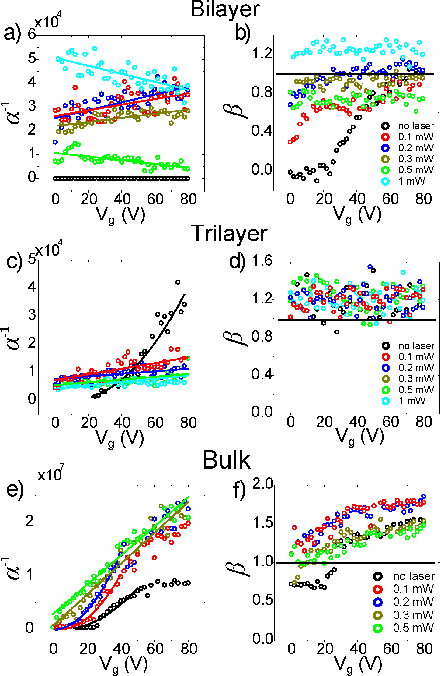
Starting with dark conditions, the noise measurements in device I Supplemental materials (Supplemental Figure 4S) and device II (Figure 4b) suggest that the transition to a sufficiently conducting regime, with -type noise, occurs only at gates above 30-40 V. This restricts the inverse noise ( vs. ) analysis to the relatively narrow range of 40 to 80 V, where the corresponding dependence shows a linear trend, indicating HMF as the driving mechanism for LFN. However, the dispersion of the normalized noise parameters has been found to be extremely large for device I Supplemental materials (see Supplemental Figure 4S). Devices III and IV, on the other hand, exhibit a quadratic dependence of as a function of the gate voltage (see Figs. 4c) and 4e), respectively). This fact, together with the fact that in the explored gate voltage range the devices show -type noise (from the parameter analysis), allows us to point at CNF as the underlying physical mechanism driving the LFNSimoen1999 . These results allow us to separate the dark condition LFN in devices I to IV into two categories. More specifically, device I and II showed -type noise driven by HMF only above some threshold gate voltage (of about 40 V for device II and 60 V for device I Supplemental materials (see Supplemental Figures 4S and 5S)), with mainly RTN for lower gate voltages; while devices III and IV revealed approximately noise driven by carrier number fluctuations in the whole range of applied gates from 0 to 80 V (see Figure 4).
Under illumination, devices I and II show a linear dependence of . With increased photodoping, the dependence of with the gate voltage changes from RTN-type, (seen under dark conditions for gate voltages lower than 40 V), to -type across the full gate range, demonstrating how the additional photoconducting channels contribute to LFN dominated by HMF Hooge1969 . Interestingly, in device II, for the maximum illumination power of 1mW, the drain-source current dependence with gate voltage exhibits a decrease for higher gate voltages Supplemental materials (Supplemental Figure 6S shows this particular case), as well as a strong reduction of the normalized noise power (Fig.4a)). We tentatively attribute this effect to an increase in the recombination rates of the charge carriers leading to a decrease in conductance and increase in LFN. For devices III and IV, one clearly observes a transition from a quadratic dependence to a linear dependence , pointing at a crossover from carrier number fluctuationsSimoen1999 to fluctuations in the carrier mobility Hooge1969 , respectively. Note that the LFN data obtained for below (i.e. practically in the OFF state) is not used in our fits to extract , since the McWhorter model is valid only for overdrive conditions, where . Table 1 summarizes the several observations under dark and illumination conditions, electrostatic gating (for overdrive conditions), and different layer count.
| I, II | III, IV | |||
| Vg Vth | Vg Vth | Vg Vth | Vg Vth | |
| Dark | RTN | HMF | CNF | CNF |
| Light | HMF | HMF | HMF | HMF |
The observation of RTN for devices I and II under dark conditions (and low gate voltage), while devices III and IV at the same conditions show CNF, was already discussed in section B, with the effect originating from the strong dependence of the recombination time-scales for different layer numbers Wang2015V1 ; Wang2015V2 . At low gate voltages, by exciting device I and II with light, the carrier density enhancement is enough to drive 1/ noise, also of HMF character.
The observed crossover from CNF to HMF in device III and IV under laser illumination can be understood as a consequence of the percolative character of conductance in the random resistor network of MoS2 FETs Paul2016 . Within this picture, the change in the noise microscopic mechanism driven by light from CNF to HMF reflects the crossing from a regime where transport happens via hopping or tunneling between disconnected metallic puddles at the fermi-level, in the so called ”island-and-sea” representation of the carrier distribution in the MoS2 flakes, to a continuum percolation, where instead of a random network of disconnected metallic puddles there is a continuum electron sea at the fermi-level.
Further analysis of the table allows us to extract one additional observation. Under sufficient electron-doping (photodoping and high electrostatic gating), all devices show HMF. Together with the fact that electrostatic gating under dark conditions is not enough to drive devices III and IV to HMF LFN (while device I and II show HMF), strongly suggests that the intrinsic doping levels of devices I and II are higher than in devices III and IV. This observation is compatible with other reports where they observe a higher carrier density for thinner devicesBritton2013 .
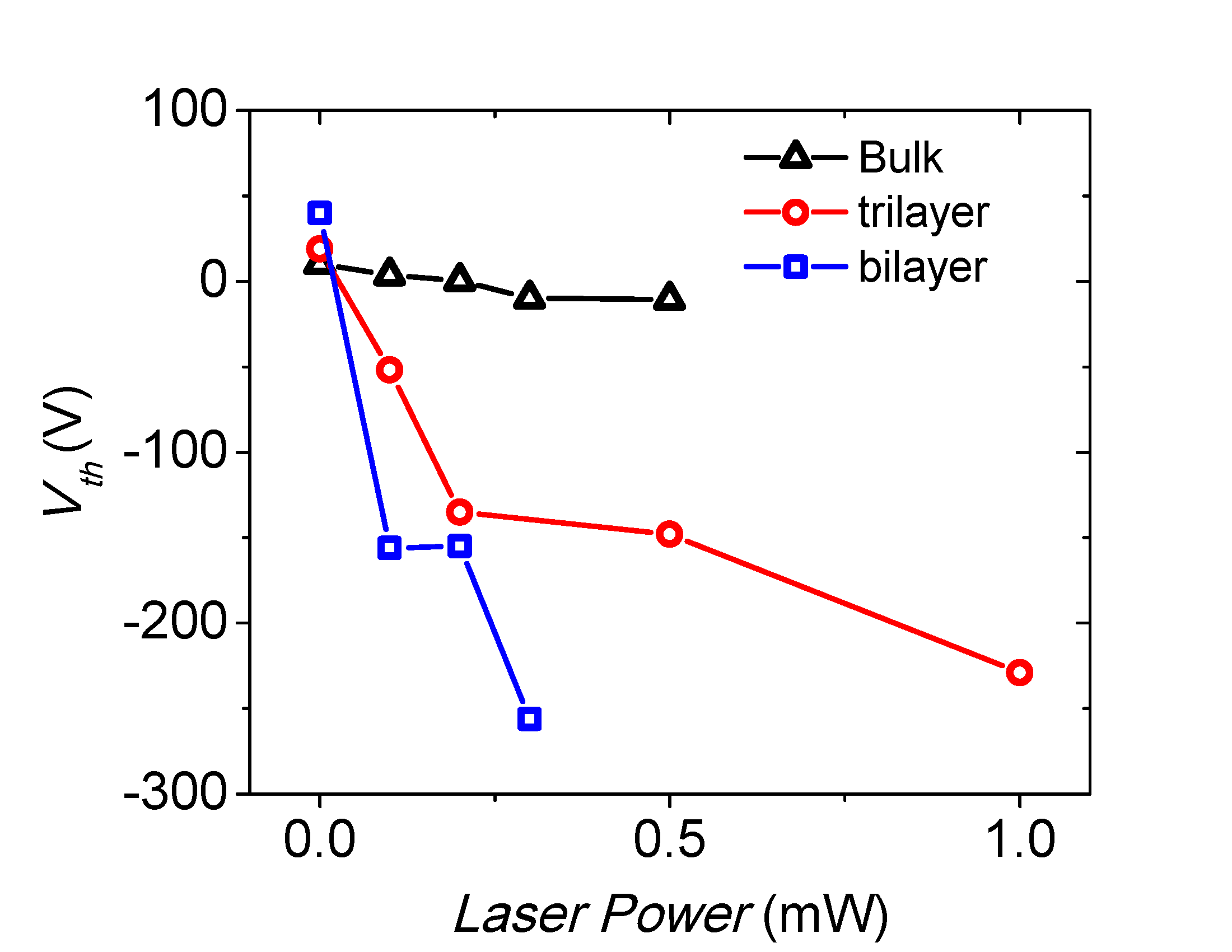
A comparison of the influence of the illumination power on (Figure 5) shows that thinner devices require lower illumination power to achieve significant photodoping, which is reflected by the shift of to lower values. is determined as the equivalent field-effect electrostatic doping required, with the use of a 250-nm-thick SiO2 dielectric, to change the MoS2 device operation from an insulating to a more conductive regime when under the specified illumination conditions (photodoping).
Gathering the several conclusive elements for the dependence of and with the layer thickness, gating, and laser illumination, the observed effects arise then from a complex interplay between the several electron-doping sources (the intrinsic doping of the flakes, the photodoping, and the electrostatic doping), and the strong decrease of the recombination time scales with decreasing layer number. RTN noise gives place to 1/-type HMF noise in the thinner devices (I and II) under sufficient electron-doping, while the thicker devices (III and IV) exhibit mainly 1/-type CNF for overdrive conditions. When in the 1/-type noise regime, we observe a crossover from CNF to HMF driven by photodoping, where by shining light the discontinuous random resistive network percolates to a continuum electron sea at the fermi level.
IV Conclusions
We have introduced a method to access different LFN regimes in MoS2 FETs by using photodoping, and identified a constraint in the transient decay time window to perform LFN studies. We believe this concept to be applicable in a much wider class of 2D materials-based FETs. Our results confirm the presence of frequency independent low-frequency generation-recombination noise, previously reported for monolayer MoS2 FETs studied under environmental conditionsSangwan2013 , attributed to either traps in the SiO2 substrate or to midgap defect states in MoS2For sufficiently thick MoS2 FETs (above bilayer), electrostatic gating in the dark state reveals -type noise driven by carrier number fluctuations, in agreement with most of the previous reports Joo2016 ; Ko2016 ; Das2015 ; Lin2015 ; Sharma2014 ; Ghatak2014 ; Xie2014 ; Renteria2014 ; Kwon2014 ; Na2014 ; Sharma2015 ; Rumyantsev2015 . In these conditions, by using photodoping with reasonably small laser powers, we are able to tune the origin of the conductance fluctuations from carrier number fluctuations to carrier mobility fluctuations. Our findings introduce then a versatile approach to investigate LFN in 2D vdW-based FETs, paving the way to overcome LFN limitations of TMD-based photodetectors and transistors.
ACKNOWLEDGEMENTS
The work in Madrid has been supported by Spanish MINECO (MAT2015-66000-P) and the Comunidad de Madrid through NANOFRONTMAG-CM (S2013/MIT-2850) grants. The work in CIC nanoGUNE has been supported by the European Union 7th Framework Programme under the Marie Curie Actions (607904-13-SPINOGRAPH), by the Spanish MINECO under Project No. MAT2015-65159-R, and by the Basque Government under Project No. PC2015-1-01.
References
- (1) A. Ambrosetti, N. Ferri, R. A. DiStasio Jr., A. Tkatchenko, Wavelike charge density fluctuations and van der Waals interactions at the nanoscale, Science 351, 1166 (2016).
- (2) A. Balandin, Low-frequency 1/f noise in graphene devices, Nat. Nanotechnol. 8, 549 (2013).
- (3) V. K. Sangwan, N. H. Arnold, D. Jariwala, T. J. Marks, L. J. Lauhon, M. C. Hersam, Low-Frequency Electronic Noise in Single-Layer MoS2 Transistors, Nano Lett. 13, 4351 (2013).
- (4) J. Renteria, R. Samnakay, S. L. Rumyantsev, C. Jiang, P. Goli, M. S. Shur, A. A. Balandin, Low-frequency 1/f noise in MoS2 transistors: Relative contributions of the channel and contacts, Appl. Phys. Lett. 104, 153104 (2014).
- (5) H-J. Kwon, H. Kang, J. Jang, S. Kim, C. P. Grigoropoulos, Analysis of flicker noise in two-dimensional multilayer MoS2 transistors, Appl. Phys. Lett. 104, 083110 (2014).
- (6) I.-T. Cho, J. I. Kim, Y. Hong, J. Roh, H. Shin, G. W. Woo Baek, C. Lee, B. H. Hong, S. H. Jin, J-H. Lee, Low frequency noise characteristics in multilayer WSe2 field effect transistor, Appl. Phys. Lett. 106, 023504 (2015).
- (7) B. Radisavljevic, A. Radenovic, J. Brivio, V. Giacometti, A. Kis, Single-layer MoS2 transistors , Nat. Nanotechnol. 6, 147 (2011).
- (8) D. Sarkar, X. Xie, W. Liu, W. Cao, J. Kang, Y. Gong, S. Kraemer, P.M. Ajayan, K. Banerjee, A subthermionic tunnel field-effect transistor with an atomically thin channel, Nature 526, 91 (2015).
- (9) H. Wang, L. Yu, Y.-H. Lee, Y. Shi, A. Hsu, M. L. Chin, L. J. Li, M. Dubey, J. Kong, T. Palacios, Integrated Circuits Based on Bilayer MoS2 Transistors, Nano Lett. 12, 4674 (2012).
- (10) S. Kim, A. Konar, W.-S. Hwang, J. H. Lee, J. Lee, J. Yang, C. Jung, H. Kim, J.-B. Yoo, J.-Y Choi, High-mobility and low-power thin-film transistors based on multilayer MoS2 crystals, Nat. Commun. 3, 1011 (2012).
- (11) M. M. Furchi, A. Pospischil, F. Libisch, J. Burgdörfer, T. Mueller, Photovoltaic Effect in an Electrically Tunable van der Waals Heterojunction, Nano Lett. 14, 4785 (2014).
- (12) S. Memaran, N. R. Pradhan, Z. Lu, D. Rhodes, J. Ludwig, Q. Zhou, O. Ogunsolu, P. M. Ajayan, D. Smirnov, A. I. Fernández-Dominguez, F. J. García-Vidal, L. Balicas, Pronounced Photovoltaic Response from Multilayered Transition-Metal Dichalcogenides PN-Junctions, Nano Lett. 15, 7532 (2015).
- (13) M. Buscema, J. O. Island, D. J. Groenendijk, S. I. Blanter, G. A. Steele, H.S. J. van der Zant, A. Castellanos-Gomez, Photocurrent generation with two-dimensional van der Waals semiconductors, Chem. Soc. Rev. 44, 3691 (2015).
- (14) F. K. Perkins, A. L. Firedman, E. Cobas, P. M. Campbell, G. G. Jernigan, B. T. Jonker, Chemical Vapor Sensing with Mono layer MoS2, Nano Lett. 13, 668 (2013).
- (15) Y-F. Lin, Y. Xu, C-Y Lin, Y-W. Suen, M. Yamamoto, S. Makaharai, K. Ueno, K. Tsukagoshi, Origin of Noise in Layered MoTe2 Transistors and its Possible Use for Environmental Sensors, Adv. Mater. 27, 6612 (2015).
- (16) Late, D. J., Liu, B., Matte, H. S. S. R., Dravid, V. P., Rao, C. N. R., Hysteresis in Single-Layer MoS2 Field Effect Transistors, ACS Nano 6, 5635 (2012).
- (17) Y. Guo, X. Wei, J. Shu, B. Liu, J. Yin, C. Guan, Y. Han, S. Gao, Q. Chen, Charge trapping at the MoS2-SiO2 interface and its effects on the characteristics of MoS2 metal-oxide-semiconductor field effect transistors, Appl. Phys. Lett. 106, 103109 (2015).
- (18) Y-C. Wu, C-H. Liu, S-Y. Chen, F-Y. Shih, P-H. Ho, C-W. Chen, C-T. Liang, W-H. Wang, Extrinsic Origin of Persistent Photoconductivity in Monolayer MoS2 Field Effect Transistors, Sci. Rep. 5, 11472 (2015).
- (19) M.-K. Joo, Y. Yun, S. Yun, Y. H. Lee, D. Suh, Strong Coulomb scattering effects on low frequency noise in monolayer WS2 field-effect transistors, Appl. Phys. Lett. 109, 153102 (2016).
- (20) S.-P. Ko, J.M. Shin, Y.J. Kim, H.K. Jang, J.E. Jin, M. Shin, Y.K. Kim, G.T. Kim, Current fluctuation of electron and hole carriers in multilayer WSe2 field effect transistors, Appl. Phys. Lett. 107, 242102 (2015).
- (21) S. R. Das, J. Kwon, A. Prakash, C. J. Delker, S. Das, D. B. Janes, Low-frequency noise in MoSe2 field effect transistors, Appl. Phys. Lett. 106, 83507 (2015).
- (22) D. Sharma, M. Amani, A. Motayed, P. B. Shah, A. G. Birdwell, S. Najmaei, P. M. Ajayan, J. Lou, M. Dubey, Q. Li, A. V. Davydov, Electrical transport and low-frequency noise in chemical vapor deposited single-layer MoS2 devices, Nanotechnology 25, 155702 (2014).
- (23) S. Ghatak, S. Mukherjee, M. Jain, D. D. Sarma, A. Ghosh, Microscopic origin of low frequency noise in MoS2 field-effect transistors, APL Materials 2, 092515 (2014).
- (24) X. Xie, D. Sarkar, W. Liu, J. Kang, O. Marinov, M. J. Deen, K. Banerjee, Low-Frequency Noise in Bilayer MoS2 Transistor, ACS Nano 8, 5633 (2014).
- (25) J. Na, M.-K. Joo, M. Shin, J. Huh, J.-S. Kim, M. Piao, J.-E. Jin, H.-K. Jang, H. J. Cho, J. H. Shimd, G.-T. Kim, Low-frequency noise in multilayer MoS2 field-effect transistors: the effect of high-k passivation Nanoscale 6, 433 (2014).
- (26) D. Sharma, A. Motayed, P. B. Shah, M. Amani, M. Georgieva, A. G. Birdwell, M. Dubey, Q. Li, A. V. Davydov, Transfer characteristics and low-frequency noise in single-and multi-layer MoS2 field-effect transistors, Appl. Phys. Lett. 107, 162102 (2015).
- (27) S. L. Rumyantsev, C. Jiang, R. Samnakay, M. S. Shur, A. A. Balandin, 1/ f Noise Characteristics of MoS2 Thin-Film Transistors: Comparison of Single and Multilayer Structures, IEEE Electron Device Lett. 36, 517 (2015).
- (28) F. N. Hooge, 1/F noise is no surface effect, Phys. Lett. A29, 139 (1969).
- (29) T. Paul, S. Ghatak, A. Ghosh, Percolative switching in transition metal dichalcogenide field-effect transistors at room temperature, Nanotechnology 27, 125706 (2016).
- (30) A. Castellanos-Gomez, M. Buscema, R. Molenaar, V. Singh, L. Janssen, H. S. J. van der Zant, G. A. Steele, Deterministic transfer of two-dimensional materials by all-dry viscoelastic stamping, 2D Mater. 1, 011002 (2014).
- (31) H. Li, Q. Zhang, C. C. R. Yap, B. K. Tay, T. H. T. Edwin, A. Oliver, D. Baillargeat, From Bulk to Monolayer MoS2: Evolution of Raman Scattering, Adv. Funct. Mater. 22, 1385 (2012).
- (32) see Supplemental Material at [URL will be inserted by publisher] for transfer curves of the devices I and IV; pulsed photocurrent response as a function of thickness; noise and photocurrent characterization of the single layer FET; and photocurrent response for devices I-IV at different laser powers.
- (33) M. Fontana, T. Deppe, A. K. Boyd, M. Rinzan, A. Y. Liu, M. Paranjape, P. Barbara, Sci. Rep. 3, 1634 (2013).
- (34) A. Allain, J. Kang, K. Banerjee, A. Kis, Electrical contacts to two-dimensional semiconductors, Nat. Mater. 14, 1195 (2015).
- (35) Baugher, B. W. H., Churchill, H. O. H., Yang, Y. Jarillo-Herrero, P., Intrinsic Electronic Transport Properties of High-Quality Monolayer and Bilayer MoS2, Nano Lett. 13, 4212 (2013).
- (36) R. Guerrero, F. G. Aliev, R. Villar, R. Ortega-Hertogs, W. K. Park, J. S. Moodera, Low frequency noise in Co/Al2O3delta(Fe)/Ni80Fe20 magnetic tunnel junctions, J. Phys. D: Appl. Phys. 35 1761 (2002).
- (37) H. Wang, C. Zhang, and F. Rana, Ultrafast Dynamics of Defect-Assisted Electron-Hole Recombination in Monolayer MoS2, Nano Lett. 15, 339–345 (2015).
- (38) H. Wang, C. Zhang, and F. Rana, Surface Recombination Limited Lifetimes of Photoexcited Carriers in Few-Layer Transition Metal Dichalcogenide MoS2, Nano Lett. 15, 8204 (2015).
- (39) H.-J. Kwon, J. Jang, S. Kim, V. Subramanian, C. P. Grigoropoulos, Electrical characteristics of multilayer MoS2 transistors at real operating temperatures with different ambient conditions, Appl. Phys. Lett. 105, 152105 (2014).
- (40) E. Simoen, C. Claeys, On the flicker noise in submicron silicon MOSFETs, Solid State Electron. 43, 865 (1999).