Observation of surface superstructure induced by systematic vacancies in the topological Dirac semimetal Cd3As2
Abstract
The Dirac semimetal phase found in Cd3As2 is protected by a rotational symmetry derived from a corkscrew arrangement of systematic Cd vacancies in its complicated crystal structure. It is therefore surprising that no microscopic observation, direct or indirect, of these systematic vacancies has so far been described. To this end, we revisit the cleaved (112) surface of Cd3As2 using a combined approach of scanning tunneling microscopy and ab initio calculations. We determine the exact position of the (112) plane at which Cd3As2 naturally cleaves, and describe in detail a structural periodicity found at the reconstructed surface, consistent with that expected to arise from the systematic Cd vacancies. This reconciles the current state of microscopic surface observations with those of crystallographic and theoretical models, and demonstrates that this vacancy superstructure, central to the preservation of the Dirac semimetal phase, survives the cleavage process and retains order at the surface.
Dirac and Weyl semimetals host low energy excitations described by the three dimensional (3-D) Dirac/Weyl Hamiltonian Young2012 . As opposed to the two-dimensional (2-D) linear dispersion found in graphene or at topological insulator surfaces CastroNeto2009 ; Hasan2010 , they host analogous ‘cones’ of three-dimensional linear dispersion, emanating from an even number of paired Weyl nodes in the bulk Brillouin zone (BZ). Where time-reversal or inversion symmetries are broken, pairs of isolated Weyl nodes of non-zero chiral charge can exist, giving rise to a Weyl semimetal phase with associated exotic physical properties Ojanen2013 ; Hosur2013 ; Potter2014 ; Baum2015 . Otherwise, Weyl node pairs are forced to coexist as chiral-charge-neutral Dirac nodes, but protected from gap opening perturbations by additional crystal symmetries. This Dirac semimetal (DSM) phase was first proposed in BiO2 and A3Bi (A = Na, K, Rb) Young2012 ; Wang2012 , and was realized in Na3Bi Liu2014 and then in the more stable Cd3As2 Liu2014a ; Neupane2014 ; Borisenko2014 .
Numerous transport observations have revealed unusual properties associated with the DSM phase in Cd3As2 He2014 ; Feng2015 ; Liang2014 ; Cao2015 ; Li2015 ; Pan2016 ; Guo2016 , including those involving surfaces, such as chirality transfer between Weyl nodes through Fermi arc surface states Moll2016 , and even possible unconventional superconductivity induced at quantum point contact interfaces Aggarwal2015 ; Wang2015 .
Dirac nodes are protected by crystal symmetries such as rotational, or non-symmorphic glide reflection symmetries. In the case of Cd3As2, they are protected by a rotational symmetry around the [001] axis Wang2013 , associated with a peculiar arrangement of systematic Cd vacancies in [001]-oriented corkscrews, in an otherwise antifluorite-like structure. This arrangement has been described in detail as part of a thorough bulk structural characterization reported by Ali et al Ali2014 . An apparent discrepancy in the position of the Dirac points (DPs) within the Brillouin zone revolves around these systematic vacancies. The DPs have been located along the (001) direction in angle-resolved photoemission spectroscopy (ARPES) investigations reported by Wang et al. Wang2013 , among others Jeon2014 ; Borisenko2014 ; Ali2014 , but along the (112) direction in work reported by Liu et al Liu2014a . This discrepancy may be attributable to a possible randomization of the Cd vacancy distribution near the cleaved surface Jeon2014 . However, it was recently demonstrated that if these Cd vacancies were to be significantly disordered or filled, the symmetry protected band crossing points, and therefore the DSM phase, would be destroyed Guo2016 ; Yuan2016 . Even with recent scanning tunneling microscopy (STM) observations Jeon2014 ; Ali2014 , it remains that no direct or indirect microscopic observation of these systematic (or random) Cd vacancies has been reported in Cd3As2, despite their central role in the formation of the DSM phase, and the position of the Dirac nodes within the BZ. Thus a gap potentially exists between the prevailing crystallographic understanding of Cd3As2 (with its theoretical implications) and existing microscopic results.
In this work we revisit the most easily attainable surface of Cd3As2, the cleaved (112) surface, using a combined approach of atomically resolved STM measurements and density functional theory (DFT) calculations. We construct an atomistic model of the (112) surface expected according to the bulk structure including systematic Cd vacancies, and show that it is predictive of our microscopic observations. This brings into agreement the crystallographic description and microscopic observations of the systematic Cd vacancy arrangement underpinning the DSM phase in Cd3As2.
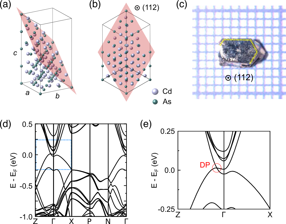
Figure 1(a) shows the conventional tetragonal Cd3As2 unit cell reported recently Sankar2015 , with a portion of the atoms cut away to illustrate the (112) surface. The pink diamond shows one of the (112) planar cuts through the unit cell, parallel to which are the natural cleavage planes. The projection of this structure looking along the normal to the cleavage planes is displayed in Fig. 1(b), showing a pseudo-hexagonal lattice. A photograph of a single crystal Cd3As2 platelet as used here is shown in Fig. 1(c). Platelets used in this work were grown as described previously Sankar2015 , and have large shiny primary facets with hexagonal shapes, corresponding to the (112) plane of the crystal. Figure 1(d) shows a bulk electronic band structure diagram calculated for this structure, with high-symmetry axes taken from the structure’s smaller primitive cell Supplement . Figure 1(e) gives a zoom-in view showing the DP located near the Fermi level between the \textGamma and Z points of the BZ.
All band structure and charge density calculations presented in this work were performed in the framework of DFT, using the projector-augmented wave (PAW) method Blochl1994 ; Kresse1999 as implemented in the VASP package Kresse1993 ; Kresse1996 ; Kresse1996a , with the Perdew-Burke-Ernzerhof exchange-correlation functional Perdew1996 and fully accounting for spin-orbit coupling. Structural optimization was performed using a 221 Monkhorst-Pack k-point mesh Pack1977 , and a kinetic energy cutoff of 300 eV. The force on each atom was less than 0.01 eVÅ-1.
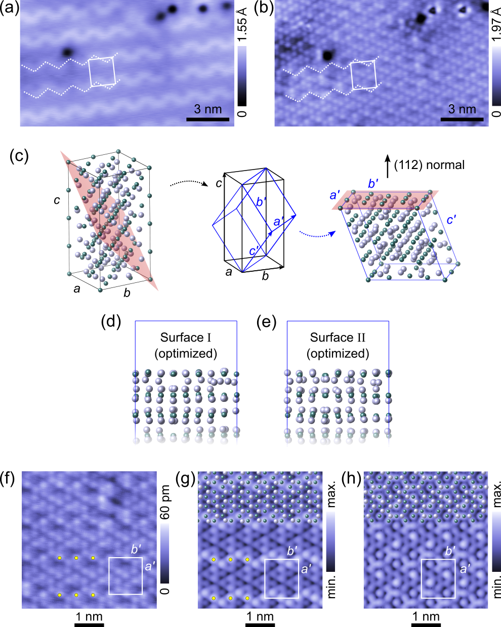
In order to perform STM measurements on the (112) surface, bulk single crystals of Cd3As2 were cleaved at room temperature in UHV conditions, before quickly being transferred to an Omicron LT-STM held at 4.5 K. An electrochemically etched tungsten tip was used, and the obtained STM images were processed using the WSxM software package WSxM . Figure 2(a) shows the typical step-terrace morphology observed in large-scale STM images taken at the (112) surface of Cd3As2. Previously, the precise position of the cleavage planes through the crystal had yet to be determined, though it has been suggested by Jeon et al., based on STM surface lattice images, that the cleaved surface terminates with an As atomic layer Jeon2014 .

We determine the precise position of the cleavage planes along the (112) normal by inspecting the step heights of the step-terrace morphology along the dashed line in Fig. 2(a). The height profile along this line is shown in Fig. 2(b). The predominant step-height, around 7.2 Å, corresponds to twice the As-As interlayer spacing parallel to the (112) normal. Figure 2(c) shows a side-view along the [111] direction of the crystal stacking. It can be seen that the basic stacking units are formed by layers of As atoms sandwiched on each side by Cd layers. Each of the observed topographic steps corresponds to a pair of these ‘trilayer sandwich’ stacking units. The pairing is due to the inequivalence of the planes separating the stacking units, which we label as cleavage planes I and II in Fig. 2(c). [And since for each type of cleavage plane, the resulting pair of cleaved surfaces on either side are structurally equivalent with one another, these labels carry over from the cleavage planes to the resulting surface: Cleavage through plane I (or II) always results in a type I (or II) surface.] As shown in Figs. 2(d) and 2(e), the main structural difference between the two surfaces is that three quarters of the systematic Cd vacancies of the Cd3As2 structure are located in the Cd atomic layer which terminates surface II. This results in linear channels of Cd vacancies arranged along the [111] direction of the conventional unit cell, indicated by red circles in Fig. 2(c).
In fact cleavage at both planes I and II is observed to occur. In Fig. 2(a), small sub-steps (marked with white arrows) can be seen protruding from the major steps, and have a height corresponding to half the major step height, or one trilayer sandwich, as is shown in the topographic line profile shown in Fig. 2(b). This indicates that both cleavage planes I and II are observable, but that one is strongly energetically preferred over the other. Here the question remains: Which cleaved surface, I or II, is the predominant one? This can be answered by detailed inspection of the observed surface atomic lattice, to which we will return below.
At this stage, we conclude that the step heights of the observed step-terrace morphology are consistent with recent descriptions of the Cd3As2 structure, and that the cleavage planes are located between adjacent Cd atomic layers, which would suggest a Cd terminated surface rather than the As surface previously suggested Jeon2014 . A Cd terminated surface is in fact more in line with previously reported x-ray photoelectron spectroscopy measurements, which have shown Cd 4d doublets dominating in intensity over As 3d doublets Liu2014a ; Sankar2015 . (The Cd 4d and As 3d levels have approximately the same photoionization cross-sections in the low photon energy range Yeh1993 .)
Figure 3 shows high-resolution STM topographs of the cleaved (112) surface. The expected pseudohexagonal atomic surface lattice and the previously reported reconstruction are observed. The most outstanding feature is a periodic, uniaxial zig-zag pattern, highlighted with dashed white lines in topographs shown in Figs. 3(a) and (b), which are acquired in the same position but using V = -0.5 and -0.1 V respectively. The overall periodicity of the surface superlattice can be characterized with a rectangular unit cell (solid white lines), with lattice parameters = 17.9 Å, = 15.6 Å. Large scale topographs show the ubiquity of this pattern over the entire measured surface Supplement . These features were not observed in STM measurements reported by Jeon et al. Jeon2014 , and possible reasons for this discrepancy are discussed below.
Fig. 3(c) shows a scheme for reorienting the Cd3As2 unit cell so that one of its faces corresponds to the rectangular surface lattice detailed in Figs. 3(a) and (b). The relation between the re-oriented and original lattice vectors is expressed by the unitary transformation , where
This alternative bulk unit cell now forms the basis of our slab model for ab initio calculations, and unlike the unit cell shown in Fig. 1(a), allows the construction of a suitable slab with a choice of (112) surface terminations facing the vacuum. Slab models terminated by surfaces I and II were constructed with a thickness of eight ‘trilayer sandwich’ stacking units Supplement . Structural optimization resulted in a small deviation from bulk-like terminations (i.e., terminations without any reconstruction) as shown in Figs. 3(d) and 3(e). A simple bulk-like termination for either surface I or II would result in either of the Cd surface lattices as shown in Figs. 2(d) and (e). Instead, in both cases surface relaxation results in a subsidence of the surface Cd lattice down to around the same level as the second (As) layer. Despite this intermingling of the surface Cd and As lattices, the number-density of observed atoms in STM images is not increased compared to that expected for a bulk-like termination. This may be because the density of states (DOS) is strongly dominated either by the Cd 5s states (conduction band) or by the As 4p states (valence band) Wang2013 , so that one lattice, either the Cd or As lattice (see below), provides the overwhelming contribution to the tunnel current and topography image. These effects greatly complicate the interpretation of STM images, since it is no longer guaranteed that surfaces I and II can be identified simply by their patterns of surface lattice vacancies.
Having obtained optimized structures for the two candidate surfaces, we calculate the partial charge density distribution in order to obtain simulated STM topographs. In order for the simulated and experimental images to be comparable, these partial charge density plots should be obtained by integrating the local density of states (LDOS) between the Fermi level and the energy corresponding to the tip voltage. However, this is not as straightforward as usual: As has been consistently reported in ARPES investigations Neupane2014 ; Borisenko2014 ; Sankar2015 and scanning tunneling spectroscopy measurements Jeon2014 ; Sankar2015 , the DPs are found 200 meV below the Fermi level Supplement . This is at odds with the expectation, based on the charge neutrality condition Wang2013 , that the Dirac nodes reside at or near the Fermi level, as is also predicted using ab initio calculations Wang2013 ; Neupane2014 ; Ali2014 . This n-type shift has been speculated to result from donor impurities, with a prime candidate being As vacancies Spitzer1966 . For the STM image shown in Fig. 3(b), taken at -0.1 eV, the bias is at ( + 100) meV. The LDOS integral to obtain the closest corresponding partial charge density map should then be made between = ( + 200) meV, and ( + 100) meV.
Simulated STM maps for candidate surfaces I and II were obtained from calculated partial charge density distributions by considering the Tersoff-Hamann model TersoffHamann and using a tip-sample distance of 4 Å Supplement . These maps are shown in Figs. 3(g) and 3(h) respectively, alongside a zoom-in STM topography image in Fig. 3(f). In each simulated map, the 2-D projected atom positions for the uppermost layer of both Cd and As are illustrated. Surprisingly, though the cleavage plane was located between two adjacent Cd layers, and the topmost Cd and As layers reside at about the same height, the dominant contribution to the observable surface lattice comes from As, possibly due to a dominance of As 4p orbitals in the DOS.
Both of the simulated STM images successfully reproduce the expected rectangular periodicity of the observed superstructure, and an additional periodicity which may correspond to the reconstruction observed by Jeon et al. Despite the challenges detailed above, we attempt to match some key features of the simulated STM images with features in the measured STM topograph. Most obviously, the simulated STM for surface I exhibits a pronounced zig-zag pattern, which matches the zig-zag appearing in the measured topographs shown in Figs. 3(a) and (b). The center-line of the zig-zag passes through a line of protrusions, several of which are marked with yellow dots in Fig. 3(g). We find corresponding atoms in the measured topograph [also marked with yellow dots in (f)], which also lie along the center-line of the zig-zag. In both the measured image and the image simulated for surface I, this line of atoms possesses the maximum topographic height. No obviously comparable zig-zag, nor any corresponding set of high protrusions can be found in the simulated STM map for surface II [Fig. 3(h)]. Based on these arguments, we identify the surface observed in measurements as surface I.
Our initial results, showing that the (112) cleavage plane is located between two adjacent Cd atomic layers, but that the terminating layer is a relaxed mixture of Cd and As atoms, clarifies upon the interpretation given by Jeon et al. It was previously thought that the observation of an apparently complete atomic surface lattice (without obvious systematic vacancies) indicated the full hcp planar lattice expected for a As terminated (112) surface Jeon2014 . While the corrugations observed in STM topographs likely correspond to the uppermost As layer, they do not directly reflect the actual surface structure.
A more concerning difference is the absence in previous work of the surface super-structure described here. This might be explained in a number of ways: i) a difference in samples, with the samples used by Jeon et al. possessing a structural phase different from that described in current models Ali2014 ; Sankar2015 . ii) a difference in the STM tip condition. In any given STM experiment, the tip apex has its own unknown orbital character, which determines the details of the tunneling transition matrix between the tip and sample, introducing unknown selection effects into topography maps. It is not impossible that different tip conditions may explain the absence in previous reports of the observed super-structure.
In our main result, we provide a microscopic description of a periodic surface superstructure caused by a pattern of systematic Cd vacancies, the symmetry of which underpins the DSM phase in Cd3As2. This reconciles the status of real-space microscopic observations with the established structure determined using x-ray diffraction (XRD), and with observations of the broad range of physical phenomena thought to accompany it. It also shows that the systematic ordering of vacancies at the surface survives the cleavage process. This surface characterization should help in the understanding of surface and interface phenomena which might be sensitively termination dependent, such as surface Fermi arcs and other possible trivial or non-trivial surface states, or possible unconventional superconductivity at heterostructure interfaces.
I Acknowledgements
The authors thank W.-L. Lee for stimulating discussions. This work was supported in part by the Ministry of Science and Technology and National Science Council of Taiwan through the following grants: MOST 104-2119-M-002-029, and NSC 101-2119-M-002-007.
References
- (1) S. M. Young, S. Zaheer, J. C. Y. Teo, C. L. Kane, E. J. Mele, and A. M. Rappe, Phys. Rev. Lett. 108, 140405 (2012).
- (2) A. H. Castro Neto, F. Guinea, N. M. R. Peres, K. S. Novoselov, and A. K. Geim, Rev. Mod. Phys. 81, 109-162 (2009).
- (3) M. Z. Hasan and C. L. Kane, Rev. Mod. Phys. 82, 3045-3067 (2010).
- (4) T. Ojanen, Phys. Rev. B 87, 245112 (2013).
- (5) P. Hosur and X. Qi, Comptes Rendus Physique 14, 857-870 (2013).
- (6) A. C. Potter, I. Kimchi, and A. Vishwanath, Nat. Commun. 5, 5161 (2014).
- (7) Y. Baum, E. Berg, S. A. Parameswaran, and A. Stern, Phys. Rev. X 5, 041046 (2015).
- (8) Z. Wang, Y. Sun, X. Q. Chen, C. Franchini, G. Xu, H. Weng, X. Dai, and Z. Fang, Phys. Rev. B 85, 195320 (2012).
- (9) Z. K. Liu, B. B. Zhou, Y. Zhang, Z. J. Wang, H. M. Weng, D. Prabhakaran, S. Mo, Z. X. Shen, Z. Fang, X. Dai, Z. Hussain, and Y. L. Chen, Science 343, 864-867 (2014).
- (10) Z. K. Liu, J. Jiang, B. B. Zhou, Z. J. Wang, Y. Zhang, H. M. Weng, D. Prabhakaran, S.-K. Mo, H. Peng, P. Dudin, T. Kim, M. Hoesch, Z. Fang, X. Dai, Z. X. Shen, D. L. Feng, Z. Hussain, and Y. L. Chen, Nat. Mater. 13, 3990 (2014).
- (11) M. Neupane, S.-Y. Xu, R. Sankar, N. Alidoust, G. Bian, C. Liu, I. Belopolski, T.-R. Chang, H.-T. Jeng, H. Lin, A. Bansil, F.-C. Chou, and M. Z. Hasan, Nat. Communs. 5, 3786 (2014).
- (12) S. Borisenko, Q. Gibson, D. Evtushinsky, V. Zabolotnyy, B. Büchner, and R. J. Cava, Phys. Rev. Lett. 113, 027603 (2014).
- (13) L. P. He, X. C. Hong, J. K. Dong, J. Pan, Z. Zhang, J. Zhang, and S. Y. Li, Phys. Rev. Lett. 113, 246402 (2014).
- (14) J. Cao, S. Liang, C. Zhang, Y. Liu, J. Huang, Z. Jin, Z. Chen, Z. Wang, Q. Wang, J. Zhao, S. Li, X. Dai, J. Zou, Z. Xia, L. Li, and F. Xiu, Nat. Communs. 5, 7779 (2015).
- (15) H. Pan, K. Zhang, Z. Wei, B. Zhao, J. Wang, M. Gao, L. Pi, M. Han, F. Song, X. Wang, B. Wang, and R. Zhang, Appl. Phys. Lett. 108, 183103 (2016).
- (16) S.-T. Guo, R. Sankar, Y.-Y. Chien, T.-R. Chang, H.-T. Jeng, G.-Y. Guo, F.-C. Chou, and W.-L. Lee, Sci. Rep. 6, 27487 (2016).
- (17) T. Liang, Q. Gibson, M. N. Ali, M. Liu, R. J. Cava, and N. P. Ong, Nat. Mater. 14, 4143 (2014).
- (18) J. Feng, Y. Pang, D. Wu, Z. Wang, H. Weng, J. Li, X. Dai, Z. Fang, Y. Shi, and L. Lu, Phys. Rev. B 92, 081306 (2015).
- (19) C. Li, L.-X. Wang, H. Liu, J. Wang, Z. Liao, and D. Yu, Nat. Communs. 6, 10137 (2015).
- (20) P. J. W. Moll, N. L. Nair, T. Helm, A. C. Potter, I. Kimchi, A. Vishwanath, and J. G. Analytis, Nature 535, 266-270 (2016)
- (21) L. Aggarwal, A. Gaurav, G. S. Thakur, Z. Haque, A. K. Ganguli, and G. Sheet, Nat. Mater. 15, 4455 (2015).
- (22) H. Wang, H. Wang, H. Liu, H. Lu, W. Yang, S. Jia, X.-J. Liu, X. C. Xie, J. Wei, and J. Wang, Nat. Mater. 15, 38 (2015).
- (23) Z. Wang, H. Weng, Q. Wu, X. Dai, and Z. Fang, Phys. Rev. B 88, 125427 (2013).
- (24) M. N. Ali, Q. Gibson, S. Jeon, B. B. Zhou, A. Yazdani, and R. J. Cava, Inorg. Chem. 53, 4062-4067 (2014).
- (25) S. Jeon, B. B. Zhou, A. Gyenis, B. E. Feldman, I. Kimchi, A. C. Potter, Q. D. Gibson, R. J. Cava, A. Vishwanath, and A. Yazdani, Nat. Mater. 13, 851 (2014).
- (26) X. Yuan, P. Cheng, L. Zhang, C. Zhang, J. Wang, Y. Liu, Q. Sun, P. Zhou, D. W. Zhang, Z. Hu, X. Wan, H. Yan, Z. Li, F. Xiu, arxiv:1601.02316v1 (2016).
- (27) R. Sankar, M. Neupane, S.-Y. Xu, C. J. Butler, I. Zeljkovic, I. Panneer Muthuselvam, F.-T. Huang, S.-T. Guo, S. K. Karna, M.-W. Chu, W.-L. Lee, M.-T. Lin, R. Jayavel, V. Madhavan, M. Z. Hasan, and F.-C. Chou, Sci. Rep. 5, 12966 (2015).
- (28) See Supplemental Material at [URL will be inserted by publisher] for an illustration of the primitive Cd3As2 unit cell and the corresponding BZ, a typical large scale topography map and a scanning tunneling spectroscopy curve obtained at the (112) surface, structures in CIF format for the re-oriented bulk and both slab models, examples of simulated STM for various tip-sample distances, and a short Python code used to obtain simulated STM images from PARCHG produced by VASP.
- (29) P. E. Blöchl, Phys. Rev. B 50, 17953 (1994).
- (30) G. Kresse, Phys. Rev. B 59, 1758 (1999).
- (31) G. Kresse and J. Hafner, Phys. Rev. B 48, 13115 (1993).
- (32) G. Kresse and J. Furthmüller, Comput. Mater. Sci. 6, 15-50 (1996).
- (33) G. Kresse and J. Furthmüller, Phys. Rev. B 54, 11169 (1996).
- (34) J. P. Perdew, K. Burke, and M. Ernzerhof, Phys. Rev. Lett. 77, 3865-3868 (1996).
- (35) J. D. Pack and H. J. Monkhorst, Phys. Rev. B 16, 1748-1749 (1977).
- (36) I. Horcas, R. Fernández, J. M. Gómez-Rodríguez, J. Colchero, J. Gómez-Herrero, and A. M. Baro, Rev. Sci. Instrum. 78, 013705 (2007).
- (37) J.-J. Yeh, Atomic Calculation of Photoionization Cross-Sections and Asymmetry Parameters, AT&T Bell Laboratories (Gordon and Breach Science Publishers, Langhorne PA, 1993).
- (38) D. P. Spitzer, G. A. Castellion, and G. Haacke, Journal Appl. Phys. 37, 3795-3801 (1966).
- (39) J. Tersoff and D.R. Hamann, Phys. Rev. Lett. 50, 1998 (1983).