Direct laser written polymer waveguides with out of plane couplers for optical chips
Abstract
Optical technologies call for waveguide networks featuring high integration densities, low losses, and simple operation. Here, we present polymer waveguides fabricated from a negative tone photoresist via two-photon-lithography in direct laser writing, and show a detailed parameter study of their performance. Specifically, we produce waveguides featuring bend radii down to , insertion losses of the order of dB, and loss coefficients smaller than , facilitating high integration densities in writing fields of . A novel three-dimensional coupler design allows for coupling control as well as direct observation of outputs in a single field of view through a microscope objective. Finally, we present beam-splitting devices to construct larger optical networks, and we show that the waveguide material is compatible with the integration of quantum emitters.
I Introduction
Applications of micro-optical systems for sensing or interferometry as well as the emerging field of quantum technology call for optical platforms yielding tight control over light propagation at ever smaller feature sizes. A successful standard route to micro-optical applications are nanofabricated waveguides on chips Bogdanov.2017 , allowing, for example, the observation of quantum walks of correlated photons in two-dimensional waveguides Poulios.2014 or first approaches to optical quantum information processing Politi.2009 . In order to extend optical microsystems to three dimensions, the method of direct laser writing (DLW) offers structuring of waveguides in glass and recently also diamond Hadden.20170120 for, e. g., boson sampling Crespi.2013 or simulating environment-assisted quantum transport Biggerstaff.2016 . Due to a small change in the index of refraction between waveguide core and surrounding medium, such waveguides can guide light and allow for evanescent wave coupling Szameit.2007 , but at the same time are restricted to feature sizes large compared to the wavelength. Beyond small changes within an optical medium, DLW allows for writing three-dimensional polymer structures that have been used, for example, to connect two photonic chips via laser-written interconnects Lindenmann.2015 .
Combining such waveguides with quantum emitters is an important step toward quantum optical applications. Nitrogen-vacancy-centers (NVC) in diamond, for example, have been shown to emit single photons at room temperature Gruber.1997 , to yield coherent access to a single electron’s spin Jelezko.2004 , and to violate, in a loophole-free setup, Bell’s inequality Hensen.2015 . Quantum emitters have been integrated into micro-optical networks by structuring waveguides in the same substrate also housing quantum emitters, such as diamond RiedrichMoller.2014 ; Mouradian.2015 ; Momenzadeh.2015 or semiconductor materials Javadi.2015 ; or, alternatively, by immersing pre-characterized quantum emitters embedded in nanoparticles into waveguides, highly facilitated by the availability of pick-and-place schemes Schell.2011 ; Liebermeister.2014 ; LarsLiebermeister.2016 ; Shi.2016 ; Schell.2014 ; Sartison.2017 ; Faez.2014 .
Here, we present the fabrication and detailed parameter studies of three-dimensional optical waveguides with high refractive index contrast showing tight mode-guiding in a low-loss polymer on glass substrates. Our waveguides go beyond existing structures in several respect. First, DLW allows combining extended planar sections laid onto the substrate with three dimensional structures. Consequently our waveguides allow combining large scale, stable networks with, e. g., out-of-plane coupling. Second, we exploit the latter to realize a novel coupler design facilitating simultaneous addressing and imaging of waveguide in- and outputs through the glass substrate using a single microscope objective, while all other sides of the substrate are still available for further manipulation. This enables, for example, controlled addressing and simultaneous direct observation of complex quantum optical experiments in one field of view of a microscope objective. Third, due to the high refractive index contrast between waveguide and air, the mode field is tightly confined by the waveguide. Finally, we show that the waveguides are in principle capable of integrating individual quantum emitters, such as NVC in nano-diamonds.
We engineer structure sizes small compared to the waveguide length, such as bend radii as small as several or beam splitting structures of lengths smaller than for total waveguide lengths of several . This allows for high integration densities, which is challenging for waveguides inscribed into glass. In contrast to systems using optical fibers and grating couplers to address the network ports, the minimum distance of our couplers is only limited by the coupler size much smaller than the diameter of an optical fiber. Thus, we can fabricate networks with a very small footprint. As a simple example, we present Y-beam splitters and systematically investigate their fabrication parameters.
II Fabrication of the Waveguides
II.1 Design Considerations
Since our goal is to produce networks with a small footprint and moreover to integrate quantum emitters into our waveguide network, we aim for waveguides having a tight mode confinement in the waveguide. These air-clad, bare waveguides on glass substrate are designed to have an almost rectangular cross section of approximately . Furthermore, the waveguide layout is designed to have all ports of the network in one field of view of our microscope using perpendicular coupling structures, addressed through the glass substrate. Because the couplers’ end facets are at the interface of resist and substrate, no facet preparation is necessary.
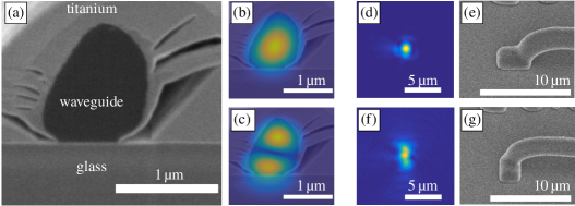
Fig. 1 (a)-(c) show the scanning electron microscope (SEM) image of the cross section of a typical waveguide with the simulated, guided TE-like waveguide modes. The intensity distribution measured at each output port depends on the specific shape of the outcoupling structure (Fig. 1 (d)-(g)). In the case of a coupling structure parallel to the waveguide the imaged intensity distribution resembles a Gaussian, while in the case of the coupling structure perpendicular to the waveguide the intensity distribution exhibits multiple spatial modes, probably originating from the coupler itself. As the transition from the waveguide to the coupling structure is not fully adiabatic for the light mode, admixtures from various spatial modes are in fact expected.
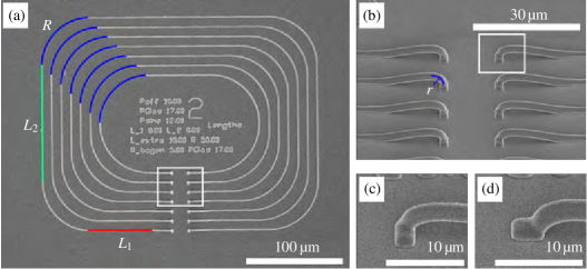
For fabrication, we use the negative tone photoresist EpoClad 50 (Microresist). The resulting waveguides comprise two types of sections. The planar waveguide itself, guiding light parallel to the substrate surface, and the coupling structure rotating the light’s propagation direction out of plane to be perpendicular to the substrate surface, as shown in Fig. 2. The coupling structure is a quarter ring with radius , standing on the substrate, smoothly lowering down onto the substrate according to a -function and connecting to the waveguide. For structure stability reasons, the radius of the incoupler is as small as and the transition part has a length of . In order to increase the substrate adhesion and to improve coupling efficiency, the surface contact region is formed as coupling structures of different shapes, see Fig. 1(d)-(g) and Fig. 2(c),(d). We use shallow rectangular pads added to the end of the couplers, where we compare the performance of orientation parallel and perpendicular to the waveguide, respectively. The waveguide section is composed of straight waveguides of lengths varying between and , and between and , connected by four quarter rings, having radius . As an example, a typical set of waveguides in stadium configuration is shown in Fig. 2. The waveguides feature lengths up to , bend radii (see Fig. 2) down to with a total insertion loss as low as , enabling high integration densities. The three-dimensional coupling structures have a total height of and a length of , having a total coupling efficiency of at least . The insertion loss is at present dominated by in- and outcoupling loss and mode mismatch at the connection of differently shaped waveguide sections.
II.2 Fabrication Process
The substrates are silica coverslips (Menzel Glaeser, thickness ), initially cleaned in an ultrasonic bath (acetone, isopropanol, deionized water, each) and dried with nitrogen.
After a short dehydration bake, the coverslips are cleaned for in an oxygen plasma.
The photoresist is dropcast onto the coverslips, baked for at on a contact hotplate and cooled down natively.
For direct laser writing, a commercial system (Photonic Professional GT, Nanoscribe) is used with an immersion oil objective (63x, ). This system uses an ultrashort pulsed laser with a center wavelength of , a pulse length between and , and a repetition rate of .
We typically write with speeds of and laser powers between and (in front of the objective), composing each waveguide of four parallel trajectories.
Finally, the samples are stored overnight at room temperature for post exposure bake, developed in mr-Dev 600 (Microresist), rinsed with isopropanol and dried with nitrogen.
III Transmission and Coupling Properties
In order to check if the waveguides are suited for construction of networks with integrated emitters, knowledge about transmission and coupling properties is crucial. Particularly, the contributions of coupling losses, which will, for example, reduce the amount of light exciting a nano-emitter, and losses per length, which will attenuate the emitted signal of nano-emitters, are important to know. While the former can usually be compensated for by larger laser powers, the latter poses strong constraints on, e. g., the level of correlations detectable.
III.1 Experimental Setup and Methods
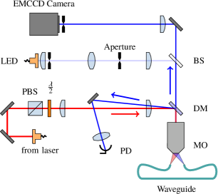
We characterize insertion loss of the waveguides and intensity distributions of the transmitted light using a homebuilt microscope (see Fig. 3). It features an objective with and a motorized stage holding the waveguide sample for scanned measurements.
| Average insertion loss | ||
|---|---|---|
| Maximum loss coefficient | ||
| Coupling loss | ||
| Damping |
In order to quantify insertion loss and transmitted mode, a single-mode infrared laserbeam () is focused onto the incoupling port of the waveguide. Each input port is scanned in a position range of approximately by moving the sample-stage with a resolution of , while keeping the incoupling laser position fixed (see Visualization 1 for a video of an input-port scan). The light transmitted is separated via a mirror and sent to a calibrated photodiode. The photodiode signals for each scan thus yield a two-dimensional image of integrated output intensities, see Fig. 4. The insertion loss is defined as the ratio of transmitted and injected power. In order to correct the transmission for background due to, e. g., scattering, the transmitted power is calculated as difference between maximum and minimum power for each scan field.
The position resolved transmitted intensity distribution for each incoupling position is obtained by imaging the waveguides’ ports by an EMCCD camera (iXon3 DU-885K, Andor), see Fig. 4, where also light scattered from the waveguides would be visible.
III.2 Waveguide Damping and Loss Coefficients
Insertion loss can originate from three distinct sources. First, losses occur at the in- and outcoupling ports due to mode mismatch with the free space beam and due to the small coupler geometry. Second, absorption or scattering in the waveguides can lead to a constant loss per unit length, while, third, at each interface between straight and bent waveguide parts losses can occur due to improper mode matching. In order to estimate the contributions of loss per length, loss due to the bend radius, and loss due to imperfect mode-matching, we compare three different sets of waveguides. First we extract the length dependent loss coefficient and the loss due to coupling through variation of the waveguide length similar to the cutback technique.
Therefore, in a first set of waveguides, shown in Fig. 2, the lengths and of the waveguides are increased for two different curvature radii , while keeping the number of straight-to-bent transitions constant. Within our measurement uncertainty we do not observe an increased loss, neither when increasing the total waveguide length by a factor of three to , see Tab. 1, nor when changing the bend radius from to , consistent with Fig. 7. The transmission data taken does not show any obvious trend. We thus give the average insertion loss and estimate an upper bound for the loss per unit length by using our measurement uncertainty as maximum loss for the longest waveguide. Thus the loss per unit length is smaller than for a bend radius of and smaller than for . Alternatively, we fit linear damping on a logarithmic scale (see Tab. 1 for the parameters), which yields reasonable values for the coupling loss, but the parameters for damping are compatible with zero damping, or even show negative damping.
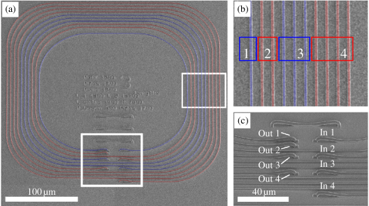
Since the damping coefficient is not reliably determined from this set of waveguides, the length of the waveguides is increased even more by coiling up the waveguides with fixed curvature radius , keeping the dimensions below , the range accessible by the Nanoscribe’s piezo stage.
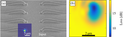
One field containing a set of these test structures is shown in Fig. 5.
We fabricate five identical sets of these fields. Since two of the fields do not guide light properly due to fabrication imperfections, such as improper automated localization of the interface between coverslip and photoresist during DLW, we evaluate the other three fields in the following.
The total lengths of the waveguides shown are , , , and respectively.
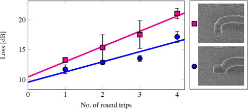
The losses observed are shown in Fig. 6 and are proportional to the number of turns or, equivalently, number of transitions from straight to bent waveguide parts and vice versa. To illustrate the effect of different coupler geometries, we compare the results for two differently oriented rectangular couplers.
For parallel coupling structures we get an extrapolated combined in- and outcoupling loss of and a loss per round trip of , for perpendicular coupling structures the in- and outcoupling loss is and the loss per round trip is .
The incoupling loss for both structures coincides but the loss per round trip differs, which is likely due to the perpendicular coupling structure itself causing increased loss for the adjacent waveguide.
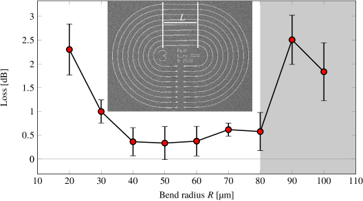
The fabrication of waveguide networks with high integration density requires small bend radii, limited eventually by losses of the light mode from the bent waveguide. To investigate such bend induced loss, we study a third set of structures and vary the bend radius from to . One field containing these waveguides is shown in Fig. 7. Again, five copies of this field are fabricated and all of them are evaluated. The data from different writing fields containing the structures shown in Fig. 7 show the same scaling with bend radius , however, they differ by an offset against each other. Therefore, we subtract the minimum insertion loss measured in one field from all waveguides in this respective field, to extract the bend induced loss. For radii between and , the bend loss shows the expected behavior: it decreases with increasing radius up to by approximately and shows approximately no further change for larger radii. Above , the bend loss increases again. Since this behavior is not expected from waveguide theory, this part of Fig. 7 is shaded in gray. Possible reasons for this unexpected increase can include tensions in the structure or too small substrate adhesion, leading to local peeling. Since we are interested in small bend radii, this is not limiting for us and not further investigated. For all other measurements shown in this work, a bend radius of is used.
We conclude from these measurements that the dominant source of losses originates from imperfect mode matching between waveguide sections, where the measured value depends on the specific design of waveguide and coupling structure. Also a small foot-print of optical elements is possible with bend radii down to . These results are promising for constructing quantum optical networks with high integration density, where the in-coupling losses can be easily compensated for, while sensitive signals can be guided with low loss.
IV Fluorescence Measurements
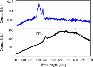
For the future we aim on integrating single quantum emitters, such as NVC in nano-diamonds, into our waveguide network. The signal of these single emitters might be masked due to fluorescence from waveguides or the substrate itself. Therefore we investigate the fluorescence of the photoresist used, EpoClad 50, upon excitation at . The resulting spectrum is shown in Fig. 8 in comparison to the emission of a single nano-diamond containing many NVC (1200 NVC/particle, fluorescent nano-diamond, Sigma-Aldrich). The resist spectrum shows two distinct peaks at wavelengths slightly below the zero-phonon-line of the NVC at on top of a flat and broad background. Integrating the total fluorescence signal, we find a resist fluorescence which is only 60% above the fluorescence level of the glass substrate used. In order to directly compare the signals from resist with NVC fluorescence, we also integrate the NVC spectrumfootnote , normalize the signals with respect to the respective excitation power and the NVC signal to the estimated number of 1200 NVC in the nano-diamond investigated. We find total fluorescence levels in the same order of magnitude for resist and a single NVC. In future work, single NVC will be integrated into the waveguide network. In fact, single emitters integrated into waveguides with a refractive index near to the substrate as well as their characterization were reported in Shi.2016 . There, it has been shown that the integration into waveguides efficiently guiding the emitted single photons increases the signal to noise ratio, facilitating coupling to single emitters also in our waveguides.
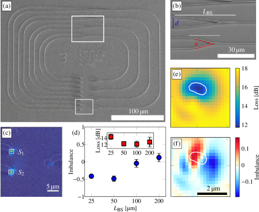
V Towards Complex Networks
Beam splitters are the most important optical element to construct waveguide networks. We fabricate and evaluate five copies of the set of Y-beam splitters shown in Fig. 9, as a simple realization for our waveguide system. The splitters differ from each other by the splitting angle, realized by varying the length over which the splitted waveguides separate to the final distance , see Fig. 9(b). The splitters shown have angles . In order to characterize the performance, the transmitted power of the whole splitter is again recorded by a photodiode as a function of input port position, yielding a two-dimensional transmission map for each output port. From these maps, a two-dimensional loss map is calculated, see Fig. 9(e). In order to estimate the imbalance for each incoupling position, we take the camera image Fig. 9(c) and calculate the imbalance as
| (1) |
where , are the integrated intensities in the white squares , in Fig. 9(c). This yields a two-dimensional map of the splitter’s imbalance, see Fig. 9(f). We identify the range of incoupling positions where the transmission is above of the maximum transmission and calculate for these pixels the average imbalance as well as its standard deviation shown in Fig. 9(d).
The insertion loss decreases with increasing beam splitter length and also the beam splitters become more balanced. A reason for the splitters’ imbalance might originate from a small structural asymmetry resulting from the writing process. This limitation, however, can be resolved through parameter optimization.
These results show that waveguide networks can be fabricated from the presented photoresist material system. By concatenating the beam splitter design shown with adjusted splitting angles, the power distribution in the network’s branches might be adjusted.
VI Conclusions
In summary, we have demonstrated up to long direct laser written waveguides with an insertion loss as low as , showing low loss for bend radii between and . The long waveguide itself is laid down onto the silica substrate, while for in- and outcoupling of light, three dimensional couplers are used. These couplers are viewed simultaneously with a single microscope objective, giving access to the whole network while leaving the other side of the substrate open for further manipulation. As a first device, we show simple Y-beam splitters with an insertion loss of and an adjustable splitting ratio via variation of the splitting region’s length.
Our next step is to integrate nano-diamonds containing NVC into our structures, which is expected to increase the signal-to-noise ratio Shi.2016 . For our photoresist, we find an autofluorescence of the same order as the NVC fluorescence. Further, we aim at scaling up the size and complexity of our network and showing interferometers and resonators. This will give access to, e. g., the phase and frequency of the transmitted photons. The versatility of the system used also facilitates combining our waveguide networks with existing photonic chips or connecting the waveguides directly to detectors, e. g. photodiodes, or light sources. The polarization of light transmitted through the waveguide network is an important degree of freedom; DLW allows access to control all waveguide parameters to tune, for instance, the polarization of the propagating light.
VII Acknowledgments
A. Landowski is a recipient of a DFG-fellowship through the Excellence Initiative by the Graduate School Materials Science in Mainz (GSC 266). We thank Michael Renner for initial support with the DLW process and Michael Schmidt for technical support in the initial phase of the project. We also acknowledge technical support by the Nano Structuring Center, TU Kaiserslautern.
References
- (1) S. Bogdanov, M. Y. Shalaginov, A. Boltasseva, and V. M. Shalaev, “Material platforms for integrated quantum photonics,” Optical Materials Express 7, 111 (2017).
- (2) K. Poulios, R. Keil, D. Fry, J. D. A. Meinecke, J. C. F. Matthews, A. Politi, M. Lobino, M. Grafe, M. Heinrich, S. Nolte, A. Szameit, and J. L. O’Brien, “Quantum walks of correlated photon pairs in two-dimensional waveguide arrays,” Physical review letters 112, 143604 (2014).
- (3) A. Politi, J. C. F. Matthews, and J. L. O’Brien, “Shor’s quantum factoring algorithm on a photonic chip,” Science (New York, N.Y.) 325, 1221 (2009).
- (4) J. P. Hadden, V. Bharadwaj, B. Sotillo, S. Rampini, R. Osellame, T. T. Fernandez, A. Chiappini, C. Armellini, M. Ferrari, R. Ramponi, P. E. Barclay, and S. M. Eaton, “Waveguide-coupled single nv in diamond enabled by femtosecond laser writing,” (2017).
- (5) A. Crespi, R. Osellame, R. Ramponi, D. J. Brod, E. F. Galvão, N. Spagnolo, C. Vitelli, E. Maiorino, P. Mataloni, and F. Sciarrino, “Integrated multimode interferometers with arbitrary designs for photonic boson sampling,” Nature Photonics 7, 545–549 (2013).
- (6) D. N. Biggerstaff, R. Heilmann, A. A. Zecevik, M. Gräfe, M. A. Broome, A. Fedrizzi, S. Nolte, A. Szameit, A. G. White, and I. Kassal, “Enhancing coherent transport in a photonic network using controllable decoherence,” Nature communications 7, 11282 (2016).
- (7) A. Szameit, F. Dreisow, T. Pertsch, S. Nolte, and A. Tünnermann, “Control of directional evanescent coupling in fs laser written waveguides,” Optics Express 15, 1579 (2007).
- (8) N. Lindenmann, S. Dottermusch, M. L. Goedecke, T. Hoose, M. R. Billah, T. P. Onanuga, A. Hofmann, W. Freude, and C. Koos, “Connecting silicon photonic circuits to multicore fibers by photonic wire bonding,” Journal of Lightwave Technology 33, 755–760 (2015).
- (9) A. Gruber, “Scanning confocal optical microscopy and magnetic resonance on single defect centers,” Science 276, 2012–2014 (1997).
- (10) F. Jelezko, T. Gaebel, I. Popa, A. Gruber, and J. Wrachtrup, “Observation of coherent oscillations in a single electron spin,” Physical review letters 92, 076401 (2004).
- (11) B. Hensen, H. Bernien, A. E. Dreau, A. Reiserer, N. Kalb, M. S. Blok, J. Ruitenberg, R. F. L. Vermeulen, R. N. Schouten, C. Abellan, W. Amaya, V. Pruneri, M. W. Mitchell, M. Markham, D. J. Twitchen, D. Elkouss, S. Wehner, T. H. Taminiau, and R. Hanson, “Loophole-free bell inequality violation using electron spins separated by 1.3 kilometres,” Nature 526, 682–686 (2015).
- (12) J. Riedrich-Moller, C. Arend, C. Pauly, F. Mucklich, M. Fischer, S. Gsell, M. Schreck, and C. Becher, “Deterministic coupling of a single silicon-vacancy color center to a photonic crystal cavity in diamond,” Nano letters 14, 5281–5287 (2014).
- (13) S. L. Mouradian, T. Schröder, C. B. Poitras, L. Li, J. Goldstein, E. H. Chen, M. Walsh, J. Cardenas, M. L. Markham, D. J. Twitchen, M. Lipson, and D. Englund, “Scalable integration of long-lived quantum memories into a photonic circuit,” Physical Review X 5 (2015).
- (14) S. A. Momenzadeh, R. J. Stohr, F. F. de Oliveira, A. Brunner, A. Denisenko, S. Yang, F. Reinhard, and J. Wrachtrup, “Nanoengineered diamond waveguide as a robust bright platform for nanomagnetometry using shallow nitrogen vacancy centers,” Nano letters 15, 165–169 (2015).
- (15) A. Javadi, I. Sollner, M. Arcari, S. L. Hansen, L. Midolo, S. Mahmoodian, G. Kirsanske, T. Pregnolato, E. H. Lee, J. D. Song, S. Stobbe, and P. Lodahl, “Single-photon non-linear optics with a quantum dot in a waveguide,” Nature communications 6, 8655 (2015).
- (16) A. W. Schell, G. Kewes, T. Schröder, J. Wolters, T. Aichele, and O. Benson, “A scanning probe-based pick-and-place procedure for assembly of integrated quantum optical hybrid devices,” Review of Scientific Instruments 82, 073709 (2011).
- (17) L. Liebermeister, F. Petersen, A. v. Münchow, D. Burchardt, J. Hermelbracht, T. Tashima, A. W. Schell, O. Benson, T. Meinhardt, A. Krueger, A. Stiebeiner, A. Rauschenbeutel, H. Weinfurter, and M. Weber, “Tapered fiber coupling of single photons emitted by a deterministically positioned single nitrogen vacancy center,” Applied Physics Letters 104, 031101 (2014).
- (18) Lars Liebermeister, Niko Heinrichs, Philipp Altpeter, Florian Böhm, Toshiyuki Tashima, Martin Zeitlmair, Harald Weinfurter, and Markus Weber, “Design, fabrication, and optical characterization of photonic waveguides for broadband evanescent sensing,” .
- (19) Q. Shi, B. Sontheimer, N. Nikolay, A. W. Schell, J. Fischer, A. Naber, O. Benson, and M. Wegener, “Wiring up pre-characterized single-photon emitters by laser lithography,” Scientific reports 6, 31135 (2016).
- (20) A. W. Schell, T. Neumer, Q. Shi, J. Kaschke, J. Fischer, M. Wegener, and O. Benson, “Laser-written parabolic micro-antennas for efficient photon collection,” Applied Physics Letters 105, 231117 (2014).
- (21) M. Sartison, S. L. Portalupi, T. Gissibl, M. Jetter, H. Giessen, and P. Michler, “Combining in-situ lithography with 3d printed solid immersion lenses for single quantum dot spectroscopy,” Scientific reports 7, 39916 (2017).
- (22) S. Faez, P. Türschmann, H. R. Haakh, S. Götzinger, and V. Sandoghdar, “Coherent interaction of light and single molecules in a dielectric nanoguide,” Physical Review Letters 113, 213601 (2014).
- (23) The NVC spectrum does not change for a single NVC, since the phonon broadening is homogeneous.