The Next SRF Technologies
Talk presented at the International Workshop on Future Linear Colliders (LCWS2016),
Morioka, Japan, 5-9 December 2016.
C16-12-05.4.
Abstract
In this talk, I introduce the proposed next superconducting radio-frequency (SRF) technologies that will make it possible to achieve much higher accelerating electric field than the present SRF technologies. Audiences are assumed to be non-experts. We start from a brief review of basics of SRF, history of the high gradient technologies and the layered structure behind it. The multiple benefit of the layered structure is introduced. We then move to the next SRF technologies: superconductor-superconductor (SS) structure and superconductor-insulator-superconductor (SIS) structure. We discuss the SS structure in detail. Experimental results are also introduced and compared with theoretical considerations.
pacs:
I Introduction
Superconducting radio-frequency (SRF) cavities accelerate electrons by using the electric field parallel to the axis. The average electric field that the charged particle sees during transit is called the accelerating field . As increases, the necessary accelerator length to achieve a target particle energy decreases. At the same time, we want to reduce dissipation at the inner surface of the cavity: a small surface resistance or a large quality factor is necessary. Thus these two parameters, and , are used to describe performances of SRF cavities, and performance test results are plotted on - planes.
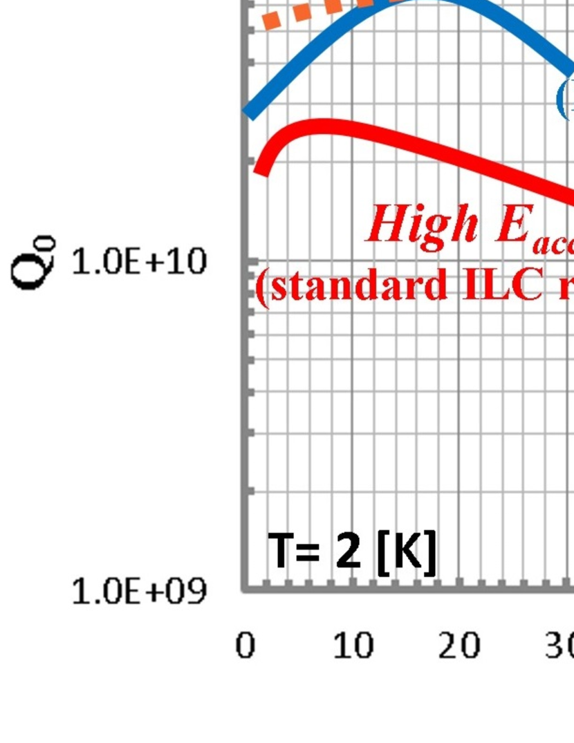
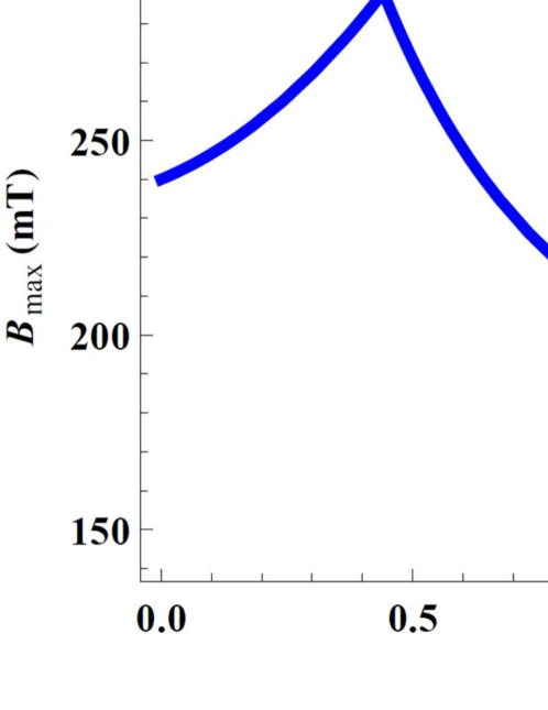
The red curve in Fig. 1 represents the rough sketch of the performance of a typical Nb cavity processed by the standard International Linear Collider (ILC) recipe. As increases, increases a little and then continues to decline. The maximum field is given by the right endpoint of the curve, , where . This is the high gradient technology established in 1990s. We have another technology established in 2010s, the so-called high-Q technology Grassellino_N_dope ; Dhakal_Ti_dope_PRAB ; Dhakal_Ti_dope_IPAC2012 . It can drastically improve , but the maximum value of is reduced. See the blue curve in Fig. 1. As increases, significantly increases, then start to decrease. The quench field is rather low compared with that of ILC recipe. The present SRF technologies consist of these two technologies: high-gradient and high- technologies. Considering cavity performances in pioneer days of SRF history (1960s), progresses in the past several decades are truly remarkable. However, we are not satisfied with the present technologies. We want to go beyond the limits of the present technologies and to realize the dotted orange curve. But, how can we do that? That’s the topic I want to talk about today. Since participants are not necessarily experts of SRF, we begin with basics of SRF focusing on high gradient applications.
II Present high-gradient technology
II.1 Basics of SRF for higher gradients
Inside the SRF cavity, the magnetic field distributes like the left figure in Fig. 2. When is small, the surface magnetic field is also small, and the magnetic flux is expelled to the outside the superconductor by the Meissner effect (see the upper right figure in Fig. 2). However, as increases, also increases, and finally vortices start to penetrate into the inside of the superconducting cavity wall (see the lower right figure in Fig. 2). This state is called the vortex state. The vortex is a normal conducting filament oscillating with the RF frequency (). Dissipation due to the vortex dynamics is so huge and can lead to quenches: the vortex state cannot be used for operations of SRF cavities. To achieve a high (or high ), a material that can withstand against the vortex penetration up to a high magnetic field should be used. That is one of the essential reasons we are using Nb as the material of SRF cavity. The lower critical field of pure Nb is ( for TESLA cavity), which is larger than other superconductors. (It should be noted that another important reason to use pure material comes from its thermal conductivity: as its purity increases, the thermal conductivity improves and stabilize cavities against the thermal breakdown.)
Now we know we should use pure Nb. But achieving such a high field is not a straight forward task, even if ultra pure Nb is available. Next we will look back the history of SRF and review how SRF researchers achieved (). The history would provide us with a clue to a higher .
II.2 History and finding of low temperature baking
When we look back the history of SRF (see figures in Ref. Ciovati_IPAC2013 ), we realize the record field had increased year by year. Various ideas had pushed up the record field: electropolishing (EP) followed by a heat treatment for hydrogen degassing saitoEP ; furuyaEP , high-pressure rinsing bernerdHPR ; saitoHPR ; kneiselHPR , clean assembly kojimaCA etc. The milestone in the high-gradient quest was the achievement of or in 1990s (the record field has changed little up to the present date since 1990s). The key was the low temperature baking kako_bake ; kneisel_40 ; ono_bake ; lilje_bake . Fig. 3(a) shows rough sketches of performances of Nb cavities with and without the low temperature baking after EP. The value of unbaked cavity (dashed black curve) suddenly drops at : the so-called high field -drop. On the other hand, the baked cavity (solid red curve) does not show such a rapid Q decay at a high field and can achieve .
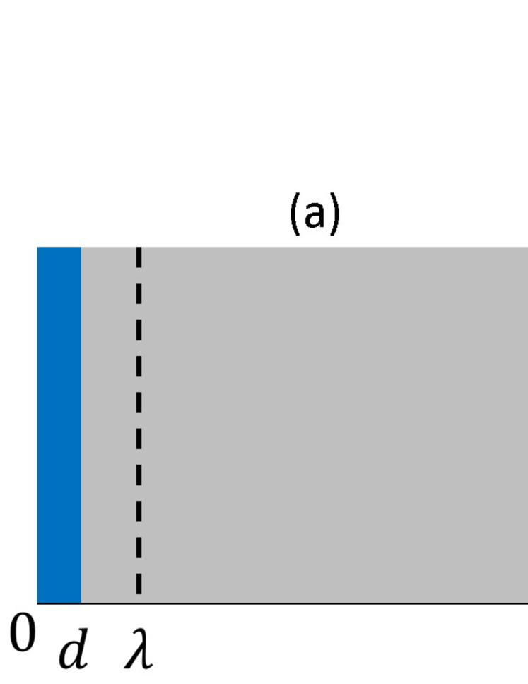
Today we know the baked Nb has the layered structure that consists of a thin dirty Nb layer and bulk clean Nb. This fact was clearly shown in the beautiful experiment using the low energy muon spin rotation (LE-SR) Romanenko_bake . Let us see the rough sketch shown in Fig. 3(b). In the unbaked Nb, the magnetic field rapidly decay as we go into the inside (see the dashed black curve). On the other hand, in the baked Nb, the magnetic field attenuates slower than the unbaked Nb in the first - and then rapidly decay at a deeper region (see the solid red curve). This means that the surface is dirty and the inside is clean. Then baked Nb can be modeled like Fig. 3(c): the layered structure that consists of the thin dirty Nb with thickness and penetration depth and bulk clean Nb with .
II.3 Multiple benefit of the layered structure
In the present day, we know many properties of the layered Nb structure through a number of theoretical studies so far. It would be beneficial to summarize them.
II.3.1 Well behaved density of states at a high field
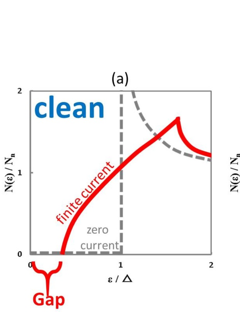
The first benefit is the well behaved density of states (DOS) of the dirty Nb at a high field Lin_Gurevich ; Gurevich_review . Fig. 4(a) and (b) show rough sketches of the DOS of clean and dirty superconductors, respectively. When the surface current is zero, the DOS of the clean and dirty superconductor are given by the common shape (dashed gray curves). As the surface current increases, the DOS of the clean superconductor becomes different from that of the dirty one (solid red curves). In particular, the gap of the clean superconductor rapidly decreases and becomes gapless before arriving at the superheating field , while the dirty superconductor still has a finite gap at (see the figures in Refs. Lin_Gurevich ; Gurevich_review ). The dirty superconductor is rather well behaved at a high field.
Use of a simple bulk dirty Nb, however, suffers a reduction of an achievable field due to a quench triggered by vortex penetration at (remind that we have repeatedly observed the quenches of impurity doped cavities at ). This difficulty is avoidable by using the layered structure that consists of a thin dirty Nb layer and a clean bulk Nb. This structure retains the of clean Nb and avoids the significant reduction of gap, because is a bulk property and given by and the gap reduction is suppressed at the surface dirty layer.
The high-field Q drop observed in the unbaked clean Nb is thought to be caused by the gap reduction due to the surface current, and the cure of high-field Q drop by the low temperature baking comes from the transformation of the surface thin layer from the clean one to dirty one Lin_Gurevich ; Gurevich_review .
II.3.2 Surface current suppression and field limit enhancement
When , the magnetic field attenuation in the surface layer is prevented by the counterflow due to the current in the substrate Kubo_APL ; Kubo_LINAC2014 ; Gurevich_AIP ; Posen_PhysRev ; Kubo_SUST . As a result, the surface current is suppressed and the theoretical field limit is enhanced, because the theoretical field limit is determined by the current density. In addition, the suppression of the surface current further delays the gap reduction to a higher field.
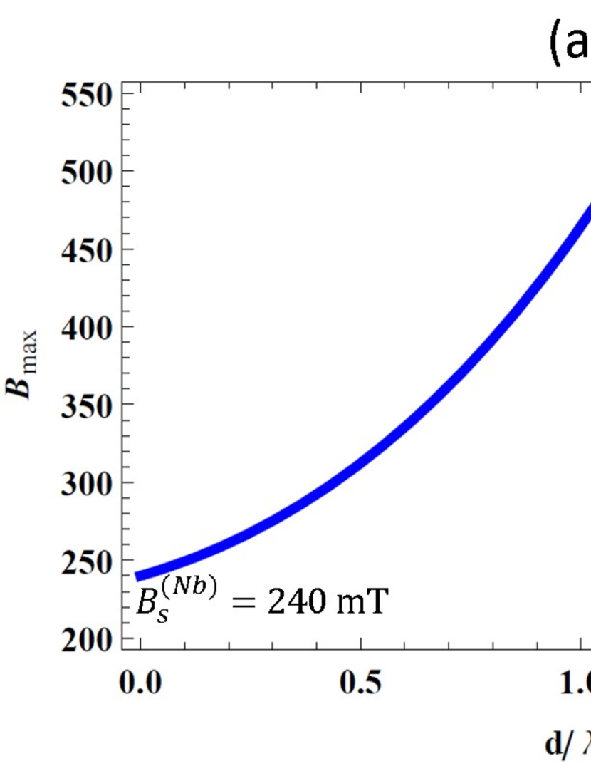
Fig. 5 shows the theoretical field limit of the layered Nb system that consists of a surface dirty Nb layer and bulk clean Nb Kubo_LINAC2014 ; Gurevich_AIP ; Kubo_SUST . It should be noted that this is the theoretical field limit for the ideal case and does not necessarily corresponds with the practically achievable field. Taking into account the existence of surface defects, the achievable field becomes much different. For example, consider the case , which is nothing but a bulk dirty Nb. In this case, the Meissner state ceases to be stable at . While the Bean-Livingstone (BL) surface barrier prevent vortex entrance, it cannot adequately protect the superconductor, because topographic and material defects covering the surface weaken the barrier. Then the practically achievable field for this case is given by instead of . In general, to go beyond , we need a “gimmick” to stop vortex penetration. Otherwise, even if the theoretical field limit is enhanced, the practically achievable field remains . As seen below, the existence of such a gimmick is the important aspect of the layered Nb structure.
II.3.3 Additional barrier against vortex penetration
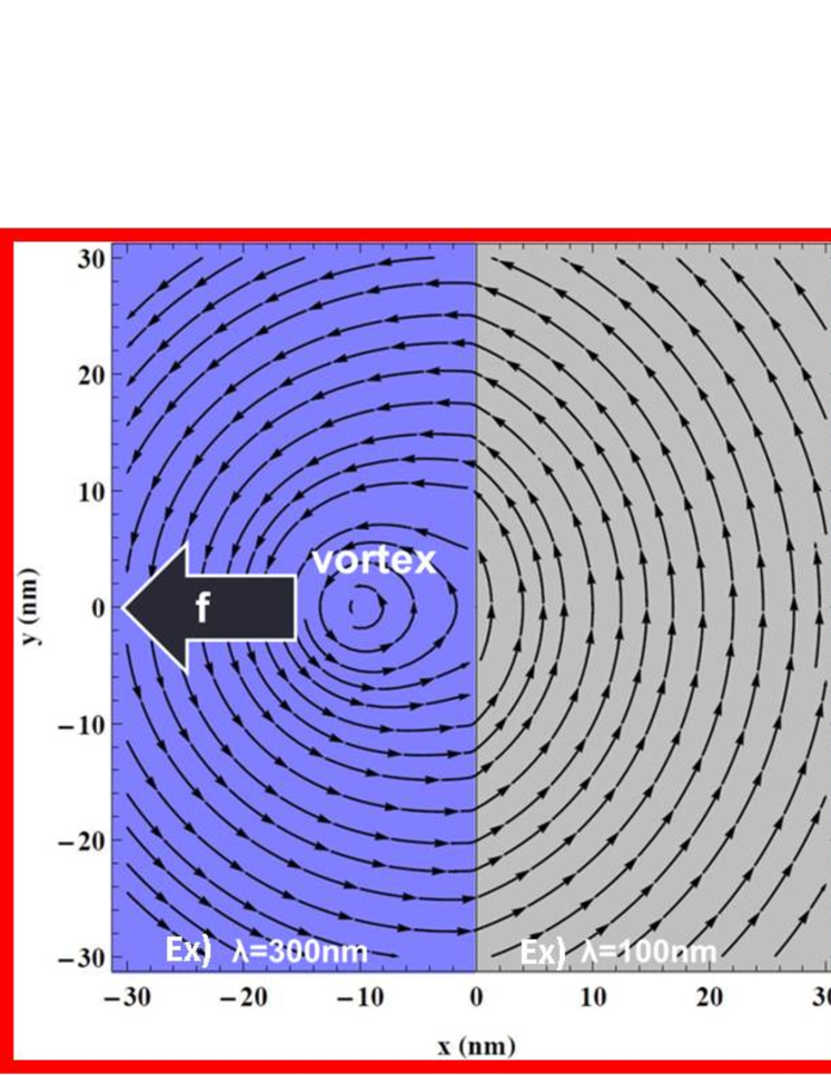
In the layered structure with , the boundary of two superconductors plays the role of the additional barrier Kubo_LINAC2014 : a vortex at the region of is expelled by the interface with the region of (see Fig. 6). This barrier originates from image vortices introduced to satisfy the boundary condition at the interface of two superconductors with different penetration depths. The major contribution comes from the nearest image with the same sign, which expels the vortex to the direction of the material with a larger penetration depth. The detailed discussion and derivation are found in Ref. Kubo_SUST . Note that the mechanism of the SS boundary barrier is different from that of the BL barrier: remind the BL barrier comes from the image with the opposite sign, which attracts the vortex to the surface. The discussion based on the Ginzburg-Landau theory is found in Ref. Checchin .
II.3.4 Surface resistance variation
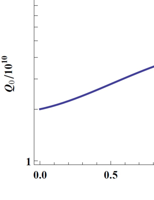
Since the current flows on both the materials when the surface layer is thinner than the penetration depth (), the surface resistance is given by a linear combination, , where and are the surface resistance of the layer material and the substrate material, respectively. The concrete expressions of the factors and are given in Refs. Gurevich_AIP ; Kubo_SUST . In particular, when the surface layer material has a smaller surface resistance , the total surface resistance can be smaller than . This effect might be related to the relatively high Q results obtained by recently developped nitrogen infusion recipe Grassellino_bake ; Grassellino_bake_arxiv . Fig. 7 shows an example of value of a layered Nb for the case the surface layer has a smaller surface resistance than the bulk.
III What’s next?
III.1 Advanced layered structures: SS and SIS
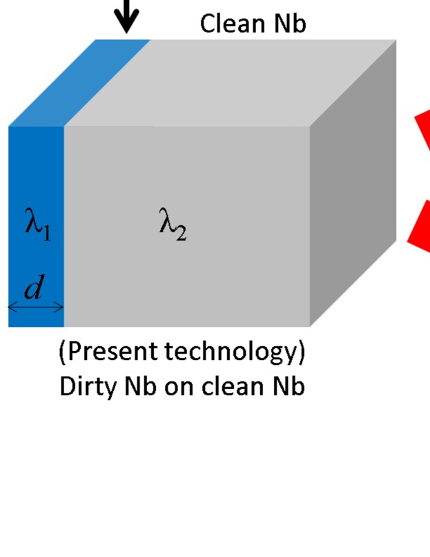
As seen in the last section, the layered Nb structure with has a number of good properties. We can generalize it to materials other than Nb. One of the promising structures consists of a bulk clean Nb substrate with a penetration depth and a thin dirty high- material with a penetration depth and thickness (see the SS and SIS structures in Fig. 8).
-
1.
Use of the thin dirty material at the surface and the clean bulk Nb as the substrate allows us to avoid the significant gap reduction effect at a high field and to retain a large Lin_Gurevich ; Gurevich_review (see Fig. 4 and Section. II.3.1 again).
-
2.
The material combination that satisfies leads to the reduction of the surface current and enhance the theoretical field limit Kubo_APL ; Gurevich_AIP ; Posen_PhysRev (see Section II.3.2 again). Fig. 9(a) shows the theoretical field limit of the SS or SIS structures that consists of surface layer and Nb substrate, where the insulator thickness is assumed to be negligible. It should be emphasized that this is nothing but a theoretical field limit for the ideal case. For a realistic case, there exist surface defects, and the practically achievable field becomes much different from Fig. 9(a). For example, consider the case , which is nothing but a bulk . Then the achievable field is given by instead of .
-
3.
The most important property equipped in the layered structures is the gimmick to stop vortex at an early stage of penetration in order for avoiding the vortex avalanches. In the SS structure, the SS boundary play the role of barrier to expel vortices if Kubo_LINAC2014 ; Kubo_SUST ; Checchin , as mentioned in the last section (see Fig. 6 and Section II.3.3 again). In the SIS structure Gurevich_APL , a much different gimmick is available. Vortices disappear in the insulator layer and do not develop into avalanches. In addition, since vortex lines disappear in the insulator layer, only a small segment of vortex that pierce the surface layer can contribute to dissipation: vortex dissipation is expected to be significantly suppressed Gurevich_AIP ; Kubo_SUST .
-
4.
The surface resistance is suppressed because a part of surface current flows in the higher material at the surface Gurevich_AIP ; Kubo_SUST (see Section II.3.4 again). Fig. 9(b) shows value of SS or SIS structure that consists of a surface layer and Nb substrate, where the insulator thickness is assumed to be negligible. The horizontal axis represents as the layer thickness .
Note here the theoretical field limit for the ideal case becomes maximum when in Fig. 9(a), but the practically achievable field does not necessarily become maximum at the same . This can be understood by considering the following example. Suppose we have a coated bulk Nb cavity with and there exists a material or topographic defect at the surface, leading to vortex penetration at a relatively low field (e. g., ). If the SS boundary barrier is so strong that vortices entering from the defect cannot go beyond the SS boundary, vortex dissipation is determined by its dynamics at . For the case this dissipation is so large that the cavity leads to a quench, we must reduce the thickness to improve the achievable field. The optimum thickness for maximizing the practically achievable field depends on the quality of material.
III.2 What we see in experiments:
muon spin rotation, magnetization measurements, and vertical tests
As I repeatedly emphasized so far, the existence of the additional gimmick that pushes up the onset of vortex penetration is more important rather than the enhancement of the theoretical field limit. Figs. 5 and 9(a) show nothing but theoretical field limits for the ideal cases that come from the surface current reduction effect of the SS and SIS and do not represent the effects of the insulator layer or the SS boundary barrier, which become significant when the surface material is not ideal. To compare the theory with experiments, we need to carefully examine non-ideal cases. We assume there exist a lot of material or topographic defects at the surface (the BL surface barrier is not perfect). Furthermore, we assume the surface material has a much smaller than Nb. We examine representative cases: and (see Fig. 10). In the following, we focus on the SS structure. As for the SIS structure, see Refs. Gurevich_AIP ; Kubo_SUST .
III.2.1
Let us begin with a simplified case: the barrier due to the SS boundary is so robust and a vortex that penetrate from the surface defect is always stopped by the barrier and does not go beyond the SS boundary. In this case, vortex penetration into the region occurs only when vortex rings are nucleated at due to a strong current density. This happens when , where the magnetic field attenuation in the surface layer is neglected because of the assumption . In SR with a deep implantation ( at ) or magnetization measurements, we will see (e.g., for Nb substrate). In vertical tests, cavities would withstand up to . While vortices may enter from the surface defect at , they are stopped at and vortex dissipation is expected to be negligible. For , vortices nucleated at flood into the material, and a cavity necessarily leads to a quench.
Next we consider the case the SS boundary barrier is moderately strong where vortices that enter from the surface defects can overcome the barrier and enter at . Then, in SR with a deep implantation and magnetization measurements, we will see . In vertical tests, we will see due to strong vortex dissipation that originate from vortices overcoming the SS boundary and moving at . According to the SR experiment Laxdal_TTC2016 ; Laxdal_LCWS2016 ; Junginger_TTC2017 , of Nb sample is given by and before and after baking, respectively: the dirty thin layer pushes up the onset of vortex penetration by . This is consistent with the above consideration where the interface between the dirty layer and the bulk clean Nb works as a moderately strong SS boundary barrier. Vertical test results are summarized in Ref. Checchin , where they also conclude baked Nb cavities pushes the onset of vortex penetration from to a field larger than . Furthermore, SR experiment results for coated bulk Nb samples are also available Laxdal_TTC2016 ; Laxdal_LCWS2016 ; Junginger_TTC2017 . Among their samples, the sample approximately corresponds with the present case (), which shows and is also consistent with the above consideration.
As we increase , the magnetic field and current density at are reduced because of the screening effect of the surface thin layer. Thus vortex nucleation at need , where is calculable if the penetration depth of this sample is known. Then we have for the case the SS boundary barrier is perfectly robust. For a moderately strong SS boundary barrier where vortices in the surface material can overcome the SS boundary barrier, we have . According to the magnetization measurements of coated bulk Nb sample Tan_SR , at for . In addition, SR experiment results of coated bulk Nb samples with thickness Laxdal_TTC2016 ; Laxdal_LCWS2016 ; Junginger_TTC2017 shows . These results are also consistent with the above consideration and demonstrate the SS boundary barrier pushes up the onset of vortex penetration.
As will be shown below, yields in SRF application. Exploring the optimum thickness in the range would be the next important task for SRF application.
III.2.2
In common with the above, we start from the case the SS boundary barrier is perfectly robust: vortices that penetrate from the surface defects are always stopped by the barrier and does not go beyond the SS boundary. Since , the surface layer can be regarded as a bulk superconductor. Vortices will start to penetrate the surface material at (strictly, ) (e.g., for thick coated Nb). These vortices, however, are stopped by the SS boundary barrier at , and the magnetic flux is absent at at this stage. Thus, in SR experiments, we cannot see any signal if the implantation depth is much larger than , even though vortices are already inside the surface layer. In vertical tests, on the other hand, cavities will suffer quenches at this stage, , because strong vortex dissipation starts at . Note that the SR with the implantation depth can confirm the fact that vortices start to penetrate at .
In the SR experiment, we can further increase . While the magnetic flux in the surface layer increases, the magnetic flux at does not change, because vortices in the surface layer cannot go beyond . The magnetic flux at starts to increase when vortex nucleation begins at . The nucleation is triggered when the current density at exceeds the depairing current (e. g., for Nb substrate). This happens the magnetic flux density in the surface material achieves . Since is approximately given by when , we find the vortex ring nucleation at start at . Thus, in SR experiments (with much deeper than ), we will see , which is the similar value as the case . Note here this for the case is not related to the SRF field limit, because vortex penetration starts at and a cavity suffers a quench due to a strong vortex dissipation: .
According to SR experiments Laxdal_TTC2016 ; Laxdal_LCWS2016 ; Junginger_TTC2017 , () coated bulk Nb sample shows , and () coated bulk Nb sample shows . In addition, there are a lot of vertical test results for thick coated bulk Nb cavity, where Posen_SUST . These all are consistent with the above consideration. It should be emphasized again that for is not related to the SRF field limit as mentioned above, but its value much larger than is quite meaningful: it indeed demonstrates the SS boundary works as a barrier.
Now we consider the case the SS boundary barrier is so weak that vortices in the surface material can overcome the barrier and go into . The vertical test results will not change: . This is because quenches are triggered by vortex penetration at and the SS boundary at does not play any role. The SR measurements results will become , because vortices in the surface material can overcome the SS boundary barrier and the flux at start to increase even when as long as the barrier is weak enough. The concrete value of depends on the strength of the SS boundary barrier.
Finally, it should be noted that all the above experiments are consistent with the existence of the SS boundary barrier, but other mechanisms can also explain the experimental results (e. g., strong pinning centers may pin vortices at the SS boundary). We do not know which mechanism is dominant. To reveal how the SS boundary prevents vortex penetration is also the next task.
III.2.3 SIS
For the SIS case, vortices that penetrate from the surface defect vanish at the insulator layer. This is robust gimmick to stop vortex penetration rather than the SS boundary of the SS structure. Furthermore, the vortex dissipation comes from the small segments that penetrate the surface layer and is expected to be significantly reduced Gurevich_AIP . See also Ref. Kubo_SUST for a review of SIS, where theoretical aspects are explained in so detail that readers can follow all the calculations.
IV Summary
We briefly reviewed basics of SRF (Section II.1) and looked back the history (Section II.2). Use of pure Nb was not enough to achieve . The low temperature baking was the key for high gradients. The recent experimental results on the low temperature baking was also introduced: the baking changes a simple clean Nb to a layered structure that consists of a thin dirty Nb and clean bulk Nb. We then summarized the multiple benefit of the layered Nb structure realized in the baked Nb (Section II.3): (1) the gap of dirty superconductor is well behaved at a high field rather than clean superconductor; (2) suppress the surface current and enhance the theoretical field limit; (3) prevent the vortex penetration by the additional barrier; (4) reduce surface resistance if the surface layer has a lower surface resistance. The multiple benefit of the layered Nb structure was generalized to materials other than Nb, and next SRF technologies, SS and SIS structures, were introduced (Section III.1). These are expected to lead to much higher gradients than the present technologies. Here we emphasized that implementation of a gimmick to stop vortex penetration is essential in order for going beyond . We then explained SS structure in detail and focusing on what we see in experiments if the surface material is not ideal one (Section III.2). Experimental data seem to support the validity of SS structure and demonstrate the SS boundary works as a barrier. To explore the optimum thickness of the surface layer () would be the next task. However, other mechanism (e.g., strong pinning centers) can also explain the experimental results. To reveal how the SS boundary stop vortices is also the next task. Detailed discussion on the SIS structure is given in Refs. Gurevich_AIP ; Kubo_SUST .
Acknowledgements.
The present work is supported by JSPS Grant-in-Aid for Young Scientists (B) 26800157, JSPS Grant-in-Aid for Challenging Exploratory Research 26600142, and Photon and Quantum Basic Research Coordinated Development Program from the Ministry of Education, Culture, Sports, Science and Technology, Japan.References
- (1) A. Grassellino et al, Supercond. Sci. Technol. 26, 102001 (2013).
- (2) P. Dhakal et al., Phys. Rev. ST Accel. Beams 16, 042001 (2013).
- (3) P. Dhakal et al., in proceedings of IPAC2012, New Orleans, Louisiana, USA (2012), p. 2426, WEPPC091.
- (4) G. Ciovati, in Proceedings of IPAC2013, Shanghai, China (2013), p. 3124, THYB201.
- (5) K. Saito et al., in Proceedings of SRF1989, KEK, Tsukuba, Japan (1989), p. 635, SRF89G18.
- (6) T. Furuya, in Proceedings of SRF1989, KEK, Tsukuba, Japan (1989), p. 305, SRF89D02.
- (7) Ph. Bernard, D. Bloess, T. Flynn, C. Hauviller, W. Weingarten, P. Bosland, and J. Martignac, in Proceedings of EPAC1992, Berlin, Germany (1992), p. 1269.
- (8) K. Saito, H. Miwa, K. Kurosawa, P. Kneisel, S. Noguchi, E. Kako, M. Ono, T. Shishido and T. Suzuki, in Proceedings of SRF1993, CEBAF, Newport News, Virginia, USA (1993), p. 1151, SRF93J03.
- (9) P. Kneisel, B. Lewis and L. Turlington, in Proceedings of SRF1993, CEBAF, Newport News, Virginia, USA (1993), p. 628, SRF93I09.
- (10) Y. Kojima et al., in Proceedings of SRF1989, KEK, Tsukuba, Japan (1989), p. 85, SRF89A07.
- (11) E. Kako et al., in Proceedings of SRF1995, Gif-sur-Yvette, France (1995), p. 425, SRF95C12.
- (12) P. Kneisel, R. W. Rth and H. - G. Kiirschner, in Proceedings of SRF1995, Gif-sur-Yvette, France (1995), p. 449, SRF95C17.
- (13) M. Ono et al., in Proceedings of SRF1997, Abano Terme (Padova), Italy (1997), p. 472, SRF97C08.
- (14) L. Lilje et al., in Proceedings of SRF1999, La Fonda Hotel, Santa Fe, New Mexico, USA (1999), p. 74, TUA001.
- (15) A. Romanenko et al., Appl. Phys. Lett. 104, 072601 (2014).
- (16) F. P. Lin and A. Gurevich, Phys. Rev. B 85, 054513 (2012).
- (17) A. Gurevich, Rev. Accel. Sci. Technol. 5, 119 (2012).
- (18) T. Kubo, Y. Iwashita, and T. Saeki, Appl. Phys. Lett. 104, 032603 (2014).
- (19) T. Kubo, in Proceedings of LINAC14, Geneva, Switzerland (2014), p. 1026, THPP074.
- (20) A. Gurevich, AIP Advance 5, 017112 (2015).
- (21) S. Posen, M. K. Transtrum, G. Catelani, M. U. Liepe, and J. P. Sethna, Phys. Rev. Applied 4, 044019 (2015).
- (22) T. Kubo, Supercond. Sci. Technol. 30, 023001 (2017).
- (23) M. Checchin, A. Grassellino, M. Martinello, S. Posen, A. Romanenko, and J. F. Zasadzinski, in Proceedings of IPAC2016, Busan, Korea (2016), p. 2254, WEPMR002.
- (24) A. Grassellino and S. Aderhold, “New Low T Nitrogen Treatments Cavity Results with Record Gradients and Q”, TESLA Technology Collaboration (TTC) meeting, Saclay, France (2016).
- (25) A. Grassellino et al., “Unprecedented Quality Factors at Accelerating Gradients up to 45 MV/m in Niobium Superconducting Resonators via Low Temperature Nitrogen Infusion”, arXiv:1701.06077 [physics.acc-ph].
- (26) A. Gurevich, Appl. Phys. Lett. 88, 012511 (2006).
- (27) R. Laxdal et al., “New insights for reaching higher gradients from muSR samples studies”, TESLA Technology Collaboration (TTC) meeting, Saclay, France (2016).
- (28) R. Laxdal, “Report from TRIUMF”, The International Workshop on Future Linear Colliders, LCWS2016, Morioka, Japan (2016).
- (29) T. Junginger, W. Wasserman, and R. Laxdal, “Insights into multilayers and new materials from muSR”, TESLA Technology Collaboration (TTC) meeting, Michigan, USA (2017).
- (30) T. Tan, M. A. Wolak, X. X. Xi, T. Tajima, and L. Civale, Scientific Reports 6, 35879 (2016).
- (31) S. Posen and D. L. Hall, Supercond. Sci. Technol. 30, 033004 (2017).