Competing weak localization and weak antilocalization in amorphous indium–gallium–zinc-oxide thin-film transistors
Abstract
We have investigated the gate-voltage dependence and the temperature dependence of the magnetoconductivity of amorphous indium–gallium–zinc-oxide thin-film transistors. A weak-localization feature is observed at small magnetic fields on top of an overall negative magnetoconductivity at higher fields. An intriguing controllable competition between weak localization and weak antilocalization is observed by tuning the gate voltage or varying the temperature. Our findings reflect controllable quantum interference competition in the electron systems in amorphous indium–gallium–zinc-oxide thin-film transistors.
Amorphous metal-oxide semiconductors have recently been studied for applications in thin-film transistors (TFTs) for large-area flexible electronics because of their electrical uniformity and fabrication advantage of room-temperature deposition and patterning Nomura04 ; Seo10 ; Gadre11 ; Chen09 . In particular, zinc oxide (ZnO) has recently attracted intense experimental and theoretical attention owing to its potential use in the emerging nanoelectronics and optoelectronics Pearton03 ; Ozgur05 ; Klingshirn07 . ZnO-based semiconductors can incorporate indium oxide as a carrier-mobility enhancer and gallium oxide or hafnium oxide as a columnar-structure suppressor for the amorphous phase in order to achieve high field-effect mobility and low off-state current of the channel Kim09 ; Kamiya10 ; Chung11 . They have become promising candidates of transparent and flexible nonvolatile memories to be integrated in system-on-panel displays Yabuta06 ; Yin08 ; Chen10 .
Aside from practical studies to achieve higher quality of amorphous indium–gallium–zinc-oxide (InGaZnO4) TFTs, investigations of their fundamental electrical properties at low temperatures are necessary for studying quantum corrections to the conductivities of these carrier systems with disorders. Quantum interference and weak localization have been explored in three-dimensional and low-dimensional electron systems in various materials Hikami80 ; Altshuler80 ; Ando82 ; Bergmann84 ; Abrahams01 ; Lee85 ; Lin02 ; Pierre03 . Indium zinc oxide (IZO) films and nanowires Shinozaki07 ; Shinozaki13 ; Thompson09 ; Chiu13 ; Kulbachinskii15 ; Xu10 in particular have raised special interest because of their potential applications in modern technologies. However, a comprehensive, in-depth study of low-temperature electrical transport in IZO is still missing, and the underlying mesoscopic and microscopic mechanisms remain largely unclear. Moreover, there are few detailed studies of low-temperature transport properties of practical IZO transistor devices. Measurements of IZO transistors at low temperatures may reveal interesting quantum-mechanical phenomena.
In this work, we present a study of the drain–source channel magnetoconductivity (MC) of an amorphous InGaZnO4 (a-IGZO) TFT measured at cryogenic temperatures. Manipulated via electric gating, the MC reveals a competition between weak localization (WL) and weak antilocalization (WAL) at small magnetic fields, where the WL component stays small but steady, while the WAL component lessens drastically with decreasing gate voltage. On the other hand, the temperature dependence of the MC also indicates a competition between WL and WAL, during which the WL component oscillates only marginally about a certain value, but the WAL component decreases gradually with increasing temperature. The competition between WL and WAL is analyzed with a quantum interference theory for two-dimensional (2D) carrier systems.
The a-IGZO TFTs based on an etch-stopper structure with passivation capping were fabricated on glass substrates. First, 300-nm-thick Ti/Al/Ti was deposited as gate electrodes by rf-magnetic sputtering, followed by a 300-nm-thick SiNx gate insulating layer using plasma-enhanced chemical vapor deposition. Next, 60-nm-thick a-IGZO was deposited by sputtering at room temperature to serve as the channel layer. After that, 200-nm-thick SiOx was deposited by sputtering as the etching stop layer. The source and drain electrodes were then formed by sputtering 300-nm-thick Ti/Al/Ti, followed by sputter deposition of 200-nm-thick SiOx as the passivation layer.
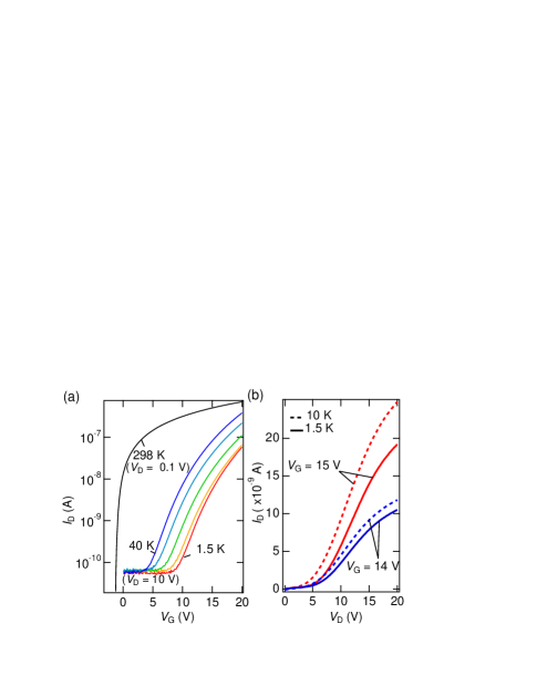
In our experiment, we performed electrical measurements on several a-IGZO TFTs, and have observed similar behaviors from them at room and cryogenic temperatures (). In this paper, we present the data collected from a representative a-IGZO TFT with a channel width () of 12 m and a channel length () of 8 m. Fig. 1a shows the drain-to-source current () of the a-IGZO TFT as functions of the gate-to-source voltage () with a fixed drain voltage () of 10 V measured at various low from 1.5 K to 40 K, while the room-temperature trace also shown in the figure was measured at V. The room-temperature electrical characteristics of the device include a fast switching time ( ms), a threshold gate voltage () of V, a subthreshold swing (S.S. ) ) of 0.45 V/decade, and a mobility of 5.6 cm2/Vs. While a small was used to operate the device at room temperature, larger was needed at cryogenic temperatures to “unfreeze” the carrier transport in the channel. Shown in Fig. 1b are the representative – traces, from which one can notice that V at either 1.5 K or 10 K drives the electrical transport away from its off-state to an intermediate regime far before its tendency towards saturation. In contrast to standard transport measurements where conductivities of thin metal films are obtained in the limit of zero driving voltage Dolan79 , moderate is needed for a-IGZO TFTs at low to initiate sufficient for valid conductivity measurements. From Fig. 1a, it can be seen that shifts to higher values as the decreases, and S.S. is seriously enlarged as well.
vs at low presented above implies a transport mechanism different from that at room temperature. In order to study the underlying physics, the magneto-transport properties of the a-IGZO TFT was investigated in the quantum diffusive regime. Shown in Fig. 2a is the normalized MC ( ) obtained at various fixed from 12.6 to 20 V as functions of the magnetic field () perpendicular to the channel plane, where the conductivity is defined as , i.e., the 2D conductivity of the channel. The traces are vertically offset for clarity with horizontal dashed lines indicating the corresponding zeros. The measurement was conducted at K with a fixed of 10 V. traces are presented only for positive below 0.2 T for a clearer view, while all of them are indeed symmetric about , like the representative trace shown in the inset over a larger range of . At V, slightly increases as increases for T, exhibiting a WL behavior. At higher , however, the trace curve bends over to WAL. These features in the curve weaken as is decreased. When goes below 15 V, the local minimum around is smeared into a plateau, while the decrease of under higher remains detectable. This implicates a -controlled quantum interference competition between WL and WAL in the a-IGZO TFT.
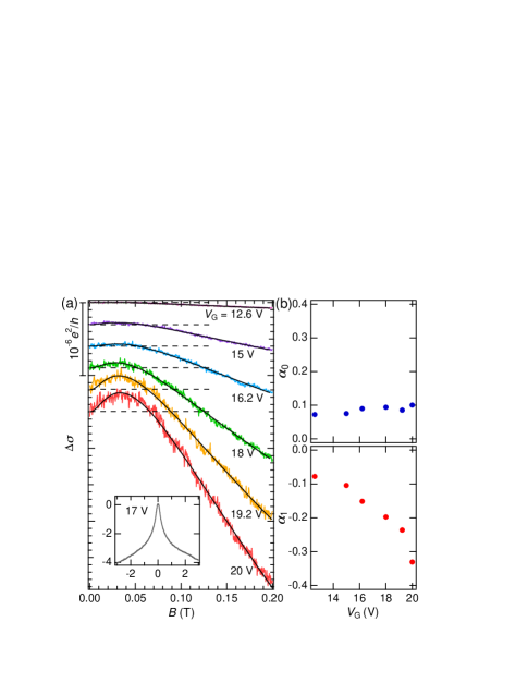
To analyze the relative strengths of WL and WAL contributions as functions of , we introduce the two-component Hikami–Larkin–Nagaoka (HLN) theory for the MC of a 2D system Hikami80 ; Lu11 ; Lu11a :
| (1) |
where is the digamma function, is the magnetic length, the prefactors and stand for the weights of WL and WAL contributions respectively, and is the corresponding phase coherence length. is a coefficient we added to the original two-component HLN equation, which will be discussed later. In the limit of pure WAL, , and for each band that carries a Berry phase McCann06 . In the limit of pure WL, , and for a usual 2D system and 1/2 for a topological surface state Lu11 . To all the -dependent traces in Fig. 2a, Eq. 1 provides excellent fits shown as solid smooth lines, and the evolutions of and obtained from the fits are summarized in Fig. 2b as functions of . When is decreased from 20 to 12.6 V, (the prefactor for WAL) decreases considerably from 0.33 to 0.08, while (the prefactor for WL) stays between 0.10 and 0.07. This indicates a drastically decreasing WAL component accompanied with a small but relatively steady WL contribution as is decreased. When reaches below 12.6 V, approaches , leading to the weakest dependence of the MC (the unitary-like behavior).
A sufficiently small value of has to be assigned to the coefficient in Eq. 1 in the analysis above, because the measured MC’s of our devices are only minuscule fractions of . For from 12.6 to 20 V at K, the a-IGZO TFT is operated between the off and on (saturation) states with low carrier densities. If the interpretation were carried out using the original HLN theory (with ), the system in the a-IGZO TFT would be regarded as a unitary class with strong magnetic scattering even for V, leaving the subtle evolutions of the WL and WAL unexplained. In order to perform a systematic analysis, the fitting procedure was started on the trace of V to find a reasonable fitting coefficient. The extremely small MC may be explained in terms of a seriously suppressed channel of conduction in the carrier system, whereas the WL and WAL phenomena can be preserved in this scenario. Specific modification of the theoretical model is needed to interpret the electrical transports in semiconductor transistors.
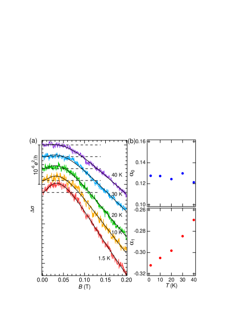
The dependence of the MC was also examined. Illustrated in Fig. 3a is vs measured at various from 1.5 to 40 K. In this experiment, at is held constant at A for different from 1.5 to 40 K by adjusting accordingly from 19.7 V to 13.9 V, through which the effect of the -dependent on transport can be compensated so that the transport conductivity at is kept the same when the dependence of is being studied. (In contrast, the transport conductivity changes with in the measurements shown in Fig. 2a.) One can find that the WL behavior at T gradually evolves into a plateau as is increased to 40 K, while the WAL behavior at higher weakens gradually with increasing . At K (with V), suffers a decrease of as is increased from 0 to 0.2 T, while with similar at 1.5 K exhibits a much smaller decrease of less than , which can be read from Fig. 2a by examining the traces of V and 15 V. This distinguishes the -dependent behaviors of WL and WAL from the -dependent behaviors observed in Fig. 2a. The data from the -dependence measurements is also analyzed using Eq. 1 with the results presented in Fig. 3b. As is increased, decreases gradually from 0.31 to 0.27, while oscillates only slightly between 0.12 and 0.13.
Gate-voltage controlled weights of WL and WAL contributions demonstrated in Fig. 2 are an intriguing feature that has not been specifically reported for IZO thin films. Electric-field controlled competition of WL and WAL has been observed in ultra-thin topological insulators Lu11 , and is theoretically interpreted in terms of the Berry phase tuned by the Fermi level with respect to the gapped surface states Lang12 . A similar mechanism may explain the WL–WAL crossover in our a-IGZO TFTs, but it remains unclear how to translate the observed WL and WAL behaviors into the details of the band structure scanned via gate-voltage tuning. It requires further theoretical research to unveil the fundamental physics of the quantum interference in a-IGZO TFTs and related devices.
The dependence of the competition between WL and WAL shown in Fig. 3 is also an important aspect in quantum interference study. A transition from a WAL to a WL state was found in three-dimensional a-IGZO films as is increased Shinozaki13 , while WAL in our device survives at higher with the WL behavior at T evolves into a plateau. According to the HLN theory for 2D systems Hikami80 , the system favors WL when the energy relaxation time decreases at higher and becomes shorter than the spin–orbit interaction time or the magnetic scattering time. However, the persistent WL component in our device is found to be accompanied with a strong WAL component, although the contribution from the latter indeed decreases as is raised. More theoretical studies are needed to understand the underlying physics of the competing WL and WAL in a-IGZO TFTs.
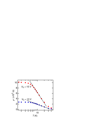
The dependence of the zero-magnetic-field channel resistivity () of the a-IGZO TFT is displayed in Fig. 4 with two representative data sets measured at and 13 V, respectively, with V. It can be seen that increases as with decreasing from 20 K to 6 K. The dependence of is reminiscent of the theoretical prediction for 2D systems with WL at low . starts to deviate from the guideline to a higher value as goes beyond 20 K, leaving the low-temperature regime where the theoretical prediction is assumed to hold. As is decreased below 6 K, on the other hand, no longer catches up the extrapolation of the guideline. The lower end of the range over which the dependence can hold is probably due to WAL. From Fig. 3b, it is clear that (the WAL prefactor) is enhanced as is decreased. Therefore, values at lower deviate from the dependence predicted for systems with only WL.
The validity of using a 2D-system theory to analyze the WL and WAL observed in our a-IGZO TFT may be inspected by considering the band energy of the a-IGZO channel Chen12 . As a positive is applied to the device, the electrons are attracted to the interface of the a-IGZO active layer and the gate insulating layer, giving a tilted quantum well with an effective width of only a small fraction of the whole a-IGZO layer thickness (60 nm). Moreover, with an effective mass of 0.35 of the free-electron mass Abe12 , the spacing between the ground and the first excited state of the carrier system in the a-IGZO channel with in the interested range is estimated to be on the order of 10–100 meV. Therefore, most of the carriers stay in their ground states at cryogenic temperatures, forming a quasi-2D system.
In summary, we have measured the MC of an a-IGZO TFT at cryogenic temperatures down to 1.5 K. With increasing from 12.6 to 20 V, the MC evolves from a unitary case to a nontrivial behavior, in which it slightly increases with increasing for T, exhibiting a WL behavior, but then decreases into a WAL behavior at higher . Analysis using the two-component HLN theory reveals a competition between WL and WAL, where the WL component stays small but steady, while the WAL component lessens drastically with decreasing . On the other hand, the dependence of the MC also indicates a competition between WL and WAL, during which the WL component oscillates only marginally about a certain value, but the WAL component decreases gradually with increasing . The gate-voltage controlled competition between WL and WAL may be interpreted in terms of the phase change in quantum interference tuned by the Fermi level in the band structure, while the temperature-controlled behavior may be explained in terms of the change in the energy relaxation time. More theoretical studies are required to fully understand the underlying physics of the competing WL and WAL in a-IGZO TFTs.
The work was supported by the Ministry of Science and Technology of the Republic of China under Grant No. MOST 102-2112-M-003-009-MY3.
References
- (1) K. Nomura, H. Ohta, A. Takagi, T. Kamiya, M. Hirano, H. Hosono, Nature 432, 488 (2004).
- (2) D. Seo, S. Jeon, S. Seo, I. Song, Appl. Phys. Lett. 97, 172106 (2010).
- (3) M. J. Gadre and T. L. Alford, Appl. Phys. Lett. 99, 051901 (2011).
- (4) M.-C. Chen, T.-C. Chang, S.-Y. Huang, H.-W. Li, Appl. Phys. Lett. 94, 162111 (2009).
- (5) S. J. Pearton, D. P. Norton, K. Ip, Y. W. Heo, and T. Steiner, Superlatt. Microstruct. 34, 3 (2003).
- (6) Ü. Özgür, Y. Alivov, C. Liu, A. Teke, M. A. Reshchikov, S. Doǧan, V. Avrutin, S. J. Cho, and H. Morkoç, J. Appl. Phys. 98, 041301 (2005).
- (7) C. Klingshirn, Phys. Status Solidi b 244, 3027 (2007).
- (8) C.-J. Kim, S. Kim, J.-H. Lee, J.-S. Park, Appl. Phys. Lett. 95, 252103 (2009).
- (9) T. Kamiya, K. Nomura, H. Hosono, Sci. Technol. Adv. Mater. 11, 044305 (2010).
- (10) W.-F. Chung, T.-C. Chang, H.-W. Li, S.-C. Chen, Appl. Phys. Lett. 98, 152109 (2011).
- (11) H. Yabuta, M. Sano, K. Abe, T. Aiba, T. Den, H. Kumomi, K. Nomura, T. Kamiya, and H. Hosono, Appl. Phys. Lett. 89, 112123 (2006).
- (12) H. Yin, S. Kim, C. J. Kim, I. Song, Appl. Phys. Lett. 93, 172109 (2008).
- (13) M.-C. Chen, T.-C. Chang, S.-Y. Huang, S.-C. Chen, Electro-chem. Solid-State Lett. 13, H191 (2010).
- (14) S. Hikami, I. Larkin, and Y. Nagaoka, Prog. Theor. Phys. 63, 707 (1980).
- (15) B. L. Altshuler, D. Khmel’nitzkii, A. I. Larkin, and P. A. Lee, Phys. Rev. B 22, 5142 (1980).
- (16) T. Ando, A. B. Fowler, and F. Stern, Rev. Mod. Phys. 54, 437 (1982).
- (17) G. Bergmann, Phys. Rep. 107, 1 (1984).
- (18) E. Abrahams, S. V. Kravchenko, and M. P. Sarachik, Rev. Mod. Phys. 73, 251 (2001).
- (19) P. A. Lee and T. V. Ramakrishnan, Rev. of Mod. Phys. 57, 2 (1985).
- (20) J. J. Lin and J. P. Bird, J. Phys.: Condens. Matter 14, R501 (2002).
- (21) F. Pierre, A. B. Gougam, A. Anthore, H. Pothier, D. Esteve, and N. O. Birge, Phys. Rev. B 68, 085413 (2003).
- (22) B. Shinozaki, K. Makise, Y. Shiname, H. Nakamura, and K. Inoue, J. Phys. Soc. Jpn. 76, 074718 (2007).
- (23) B. Shinozaki, K. Hidaka, S. Ezaki, K. Makise, T. Asano, S. Tomai, K. Yano, and H. Nakamura, J. Appl. Phys. 113, 153707 (2013).
- (24) R. Thompson, D. Li, C. Witte, and J. Lu, Nano Lett. 9, 3991 (2009).
- (25) S.-P. Chiu, J. G. Lu, and J.-J. Lin, Nanotechnology 24, 245203 (2013).
- (26) V. A. Kulbachinskii, V. G. Kytin, O. V. Reukova, L. I. Burova, A. R. Kaul, and A. G. Ulyashin, Low Temp. Phys. 41, 116 (2015).
- (27) X. Xu, A. C. Irvine, Y. Yang, X. Zhang, and D. A. Williams, Phys. Rev. B 82, 195309 (2010).
- (28) G. J. Dolan, and D. D. Osheroff, Phys. Rev. Lett. 43, 721 (1979).
- (29) H. Z. Lu, J. Shi, and S. Q. Shen, Phys. Rev. Lett. 107, 076801 (2011).
- (30) H. Z. Lu, and S. Q. Shen, Phys. Rev. B. 84, 125138 (2011).
- (31) E. McCann, K. Kechedzhi, V. I. Fal’ko, H. Suzuura, T. Ando, and B. L. Altshuler, Phys. Rev. Lett. 97, 146805 (2006).
- (32) M. Lang, L. He, X. Kou, P. Upadhyaya, Y. Fan, H. Chu, Y. Jiang, J. Bardarson, W. Jiang, E. S. Choi, Y. Wang, N.-C. Yeh, J. Moore, and K. Wang, Nano Lett. 13, 48 (2013).
- (33) T.-C. Chen, T.-C. Chang, T.-Y. Hsieh, M.-Y. Tsai, Y.-T. Chen, Y.-C. Chung, H.-C. Ting, and C.-Y. Chen, Appl. Phys. Lett. 101, 042101 (2012).
- (34) K. Abe, K. Nomura, T. Kamiya, and H. Hosono, Phys. Rev. B 86, 081202(R) (2012).