Equal-Spin Andreev Reflection in Junctions of Spin-Resolved Quantum Hall Bulk State and Spin-Singlet Superconductor
Abstract
The recent development of superconducting spintronics has revealed the spin-triplet superconducting proximity effect from a spin-singlet superconductor into a spin-polarized normal metal. In addition recently superconducting junctions using semiconductors are in demand for highly controlled experiments to engineer topological superconductivity. Here we report experimental observation of Andreev reflection in junctions of spin-resolved quantum Hall (QH) states in an InAs quantum well and the spin-singlet superconductor NbTi. The measured conductance indicates a sub-gap feature and two peaks on the outer side of the sub-gap feature in the QH plateau-transition regime increases. The observed structures can be explained by considering transport with Andreev reflection from two channels, one originating from equal-spin Andreev reflection intermediated by spin-flip processes and second arising from normal Andreev reflection. This result indicates the possibility to induce the superconducting proximity gap in the the QH bulk state, and the possibility for the development of superconducting spintronics in semiconductor devices.
A junction of superconductor and normal metal is a platform to observe superconducting proximity effect, in which the superconducting property penetrates to the normal metal. In a microscopic description of the proximity effect, an electron in the normal metal enters the spin-singlet superconductor, forming a Cooper pair with another electron with opposite spin, reflecting a hole into the normal metal, in a process called Andreev reflection (AR) Andreev (1964). In this picture, no AR is expected in the case of a fully spin polarized normal metal, however recently, theoretical and experimental studies in junctions with spin-polarized normal metal, revealed existence of the spin-triplet superconducting proximity effect Bergeret et al. (2005); Keizer et al. (2010); Asano et al. (2007a, b); Robinson et al. (2010); Visani et al. (2012); Linder and Robinson (2015). The spin-triplet proximity effect is only allowed when spin-flip processes intermediate ”equal-spin” AR, which is possible due to the presence of magnetization inhomogeneity or spin-orbit interaction Eschrig and Lofwander (2008); van Ostaay et al. (2011). Ferromagnetic metal has been utilized in experiments of superconducting spintronics to date. A semiconductor material however offers several advantages, including the control of carrier density and spin filling through electrical gating and magnetic field, and the possibility of ballistic transport in micron sized devices. Furthermore strong spin-orbit interaction can be utilized in two dimensional electron gases (2DEGs) in narrow gap semiconductors such as InAs and InSb Luo et al. (1988); de Andrada e Silva et al. (1997); Nitta et al. (1997); Heida et al. (1998). These features favor the formation of spin-polarized states when the 2DEG is in the quantum Hall (QH) regime. Indeed, there are several experimental reports focusing on superconductor-semiconductor junctions in the QH regime Takayanagi and Akazaki (1998); Eroms et al. (2005); Rickhaus et al. (2012); Komatsu et al. (2012); Wan et al. (2015); Amet et al. (2016). However, all of these experiments have focused on the spin-degenerate QH states and the spin-triplet proximity effect has yet to be experimentally addressed, despite theoretical predictions of spin-triplet supercurrent in Josephson junctions with weak links of spin resolved QH edge channels van Ostaay et al. (2011). Additionally, if the superconducting proximity gap is induced into the spin-resolved QH state, the system can be a topological superconductor Qi et al. (2010) and give a new platform to realize the Majorana Fermions Fu and Kane (2008); Hasan and Kane (2010) whose signatures have recently been reported Mourik et al. (2012); Das et al. (2012); Rokhinson et al. (2012); Nadj-Perge et al. (2014); Bocquillon et al. (2016); Wiedenmann et al. (2016); Albrecht et al. (2016); Deacon et al. (2016).
Here we report an experimental study on electron transport in junctions between spin-resolved QH states and spin-singlet superconductors. We prepared junctions consisting of a high mobility InAs quantum well (QW) with NbTi contacts. The NbTi layers are contacted to the sides of the mesa containing the QW, minimizing the damage to the 2DEG. The 2DEG possesses a large g-factor, high mobility, and strong spin-orbit interaction, all necessary ingredients for coexistence of superconductivity and spin-resolved QH states. We observe spin-resolved quantized steps at magnetic fields below the superconducting critical field, 7 T, and find that the differential conductance has a dip or a peak structure as a sub-gap feature in all QH plateau-transition regimes of filling factor between 0 to 4. Additionally, we find two side peaks on the outer side of the sub-gap feature. We conclude that the structures observed here are a result of the equal-spin AR between the spin-resolved QH bulk states and the superconductor.
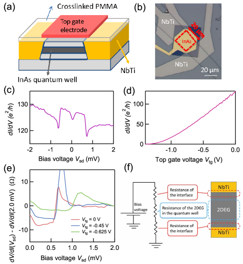
We fabricated junction devices from an InAs QW grown by molecular beam epitaxy Shabani et al. (2014a, b) with carrier density and mobility . (The material stack is represented in Supplemental Material (SM).) The cross section of the device is schematically represented in Fig. 1(a). Sputtered NbTi with the critical field of 7.0 T and the critical temperature of 6.5 K contacts the edge of the 2DEG and a top gate structure is fabricated using an insulating layer of cross-linked PMMA (see SM for details). The optical microscope photo in Fig. 1(b) shows the top view of the device. The two junctions are separated by 20 m, so this device is assumed to have two independent junctions. We measured the two-terminal differential conductance in a He3He4 dilution refridgerator with a base temperature of 50 mK.
Figure 1(c) shows the measured vs. at 0 T. The is enhanced in the range of mV. This conductance enhancement arises from AR Andreev (1964); Blonder et al. (1982) and only appears for the bias voltage in the junction less than the superconducting bulk gap energy . Therefore, we evaluate the as approximately 0.35 meV. The observation of the sub-gap feature guarantees that the junction has enough quality to study AR between the superconductor and spin-resolved QH state.
Figure 1(d) shows vs. the top gate voltage, . gradually decreases with decreasing and becomes pinched off for -1.38 V. This indicates that the top gating efficiently varies the 2DEG carrier density but not necessarily near the junction. We measured vs. for various values of to examine the effect of top gating on the sub-gap conductance. We derived the differential resistance as given by and then subtracted measured at mV to eliminate the normal state resistance including a series resistance due to the InAs QW away from the junction. The result is shown in Fig. 1(e) for three different values of =0, -0.45, and -0.625 V by the purple, blue, and green curve, respectively. It is clear to see that displays a pronounced reduction (or conductance enhancement) within the gap, and the reduction increases as is made more positive. If the top gating only varies the carrier density away from the junction, the reduction below the gap should be constant with . Therefore, the result of Fig. 1(e) indicates that the top gating is efficient enough to vary the carrier density in the InAs QW near the superconducting junction. In Fig. 1(e), to characterize the superconducting gap decreases as is made more positive. The shift is due to the change in the voltage dropped over the junctions when the series resistance of the 2DEG is altered. Schematics of the equivalent circuit for the device are shown in Fig. 1(f). In the constant voltage bias measurement, the effective junction voltage decreases as the carrier density of the QW decreases with decreasing . Herein the applied voltage of is assumed to only drop across the junctions in the saturation region. Therefore we evaluate meV. This is smaller than the value of 0.99 meV, predicted from the critical temperature with conventional BCS theory. A reduced has been reported in previous studies Irie et al. (2016), and assigned to the normal reflection in the junction as a possible origin. The normal reflection can lift the degeneracy of the gap, making the energy lower Tang et al. (1996).
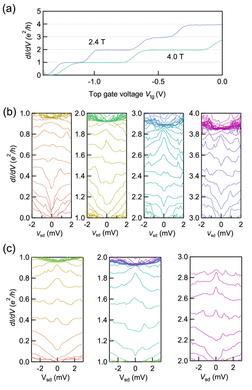
In Fig. 2(a), we present plots of measured as a function of at out-of-plane magnetic field and T. The well-defined plateaus at integer multiples of which originate from the QH edge transport are clearly seen. From this observation, it is confirmed that the applied fields are strong enough to resolve the spin degeneracy, but significantly smaller than the critical field of the NbTi, implying that the superconductivity and the spin-resolved QH states coexist.
vs. measured in the range of between -1.5 V and 0 V is represented in Fig. 2(b), and (c) for T, and T, respectively. traces measured for magnetic fields spanning the conductance range to with are shown in the separate panels to highlight the sub-gap structure in the transition regions between plateaus. For example, at T between is shown in the leftmost panel of Fig. 3(b).
In the transition regions between the conductance plateaus, we find pronounced sub-gap features appearing as a dip, a peak and then a dip at around V from the lower to the upper plateau in all panels. Similar sub-gap features are previously reported for the junctions of two NbN superconductors and a spin-degenerated QH state in an InAs QW Takayanagi and Akazaki (1998). However, the underlying physics of the sub-gap feature remains to be elucidated. More interestingly in Fig. 2(b) and (c), the center peak appears broad in some traces and even split into two in others. In addition to a center dip or peak structure we observe a side peak. For example, it is clear to see two side peaks at mV in addition to a peak at V for the curves at in the right panel of Fig. 2(c).
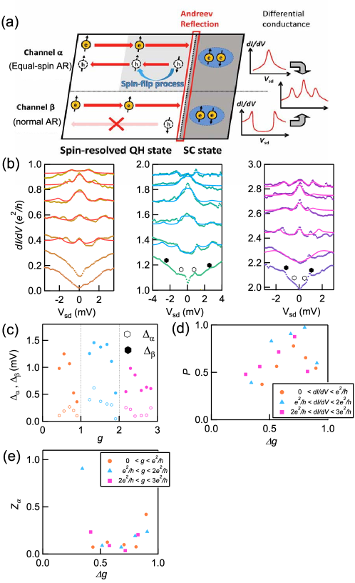
The sub-gap conductance enhancement indicated by the observation of a zero-bias peak can be assigned to AR in the junction having a low potential barrier. In contrast, if the potential barrier is so large that normal reflection is more dominant than AR, a dip rather than a peak can appear according to the Blonder, Tinkham, and Klapwijk (BTK) theory Blonder et al. (1982). Therefore we assign the peak (dip) structure observed in the plateau-transition regime to AR (normal reflection), and then the change of the sub-gap feature in Fig. 2 (b) and (c) can be simply explained by considering the change of the junction potential barrier depending on . For the transport through the QH state it is well established that the dominant contribution arises from the QH bulk state in the plateau-transition regime and from the QH edge state in the plateau regime. Herein, we deduce that the sub-gap feature, especially the peak structure is originated from AR in the junction between the superconductor and the spin-resolved QH bulk state. A finite amount of equal-spin AR can be expected for a 2DEG with strong spin-orbit interaction according to recent theoretical studies Eschrig and Lofwander (2008); van Ostaay et al. (2011). Therefore, we here assume coexistence of equal-spin AR and normal AR, corresponding to AR intermediated with and without a spin-flip process respectively, as schematically shown in Fig. 3(a).
In order to more quantitatively interpret the sub-gap features including the side peaks, we construct a model based on the BTK theory. In this theory, the normalized differential conductance of the junction, , can be written as
| , | (1) |
where and are the Fermi-Dirac distribution function, temperature, superconducting gap and the dimensionless parameter representing the potential barrier in the junction, respectively. () is the probability of the equal-spin AR (normal reflection) defined in the BTK theory Blonder et al. (1982). However, this standard BTK theory cannot explain the coexistence of side peaks and sub-gap feature as observed in Fig. 2(b) and (c). Herein, to apply the BTK theory for such cases, we assume two different transport channels in the proximity region, labeled channel in which the equal-spin AR occurs and channel with no spin-flip process. A schematic representation of the transport in these channels is shown in Fig. 3(a). The channel can generate the sub-gap features reflecting the conductance enhancement due to the equal-spin AR, while the channel can generate the side peaks reflecting the quasiparticle peaks of the superconducting bulk gap energy via normal reflection. Then, the normalized differential conductance of the junction can be written as
| (2) |
where are the normalized differential conductance of the channel , the normalized differential conductance of the channel , the parameter in the eqn. (1) of the channel and that of the channel , respectively. , and are the proximity gap energy, and the bulk gap energy, respectively. Parameter indicates the relative contribution of the two AR channels. We note that the appearance of two superconducting gaps are theoretically discussed in the case of coexistence of spin-singlet and triplet superconducting pair amplitude Burset et al. (2014, 2015). We executed numerical calculations to fit the experimental data (see SM).
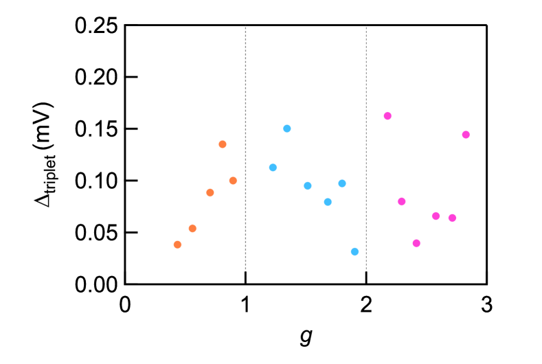
The best fitting result is shown in Fig. 3(b) by the solid lines plotted alongside the experimental data at 4.0 T. The obtained and are plotted as a function of in Fig. 3(c). for the x-axis is the differential conductance of the normal state measured at mV in units of and indexed by . is derived from the side peak positions and has a convex upward trend in each plateau-transition regime between plateaus of g= 0 and 1, 1 and 2, and 2 and 3, respectively. These values are larger than the true bulk gap due to the dissipation in the QH bulk state (the equivalent circuit is the same as shown in Fig. 1(f)). We assume that the superconducting bulk gap meV which is derived in Fig. 1(c) is unchanged with and therefore in Fig. 3(c) should be equal to . This assumption is probably valid because the observed in the plateau regime where there is no dissipation is consistent with (see SM). Then we use the same equivalent circuit model as used for evaluating to calibrate the value of and finally obtain the true proximity gap of meV as shown in Fig. 3(c) (see SM for details).
We also derived the parameters and and plot them as a function of change of in Fig. 3(c), i.e. to between plateaus in Fig. 3(d) and (e), respectively. The pink rectangles, blue triangles, and orange circles represent the parameters derived from the right, center, and left panel of Fig. 3(a), respectively. indicating the proportion of AR in channel has the maximum () and has a minimum at . Our experimental results are obtained by the two-terminal conductance measurement. Therefore the bulk contribution to the channel becomes maximum at a position displaced from and likely located between and 1. Indeed we find that the bulk contribution is maximal at which is consistent with measurement results on a Hall-bar device (see SM). These results strongly and quantitatively support that channel is comprised of the spin-resolved QH bulk state and the conductance enhancement originates from the equal-spin AR between the QH bulk state and the superconductor, while the channel is assigned to normal reflection component in the superconducting bulk gap. We note that the sub-gap feature and the side peaks have been theoretically predicted for the case of spin-singlet and spin-triplet superconducting proximity effect between a topological insulator and a spin-singlet superconductor with magnetic field Burset et al. (2015). There are a few theoretical works describing AR in the QH edge state Hoppe et al. (2000); Giazotto et al. (2005); Khaymovich et al. (2010); van Ostaay et al. (2011), but none focus on the QH state in the plateau-transition regime, and so further theoretical effort is necessary to reproduce the junction properties between superconductor and spin-resolved QH bulk state. From the topological aspects, theory predicts that the chiral topological superconductor state can be realized in superconductor-QH state junctions and therefore such junctions can be utilized to study non-Abelian statistics of the Majorana Fermions localized at the center of vortexes near the plateau-transition regime Qi et al. (2010). Our results indicate that it is possible to induce the proximity gap even in the spin-resolved QH state via equal-spin AR and so realize such chiral topological superconductivity.
In summary, we studied the transport properties of junctions between a NbTi superconductor and an InAs QW in the spin-resolved QH regime. We observed sub-gap features indicating Andreev transport arising from two channels. One equal spin Andreev reflection channel which produces peaks at zero bias, and a conventional Andreev reflection channel producing side peaks. These results indicate that junctions of NbTi and the InAs QW are a promising candidate to experimentally study the spin-triplet superconducting proximity effect in semiconductors and also topological superconductivity.
Acknowledgment
We greatly thank Y. Tanaka, P. Burset, and R. S. Deacon for fruitful discussions. This work was partially supported by Grant-in-Aid for Young Scientific Research (A) (No. JP15H05407), Grant-in-Aid for Scientific Research (A) (No. JP16H02204), Grant-in-Aid for Scientific Research (S) (No. JP26220710), JSPS Research Fellowship for Young Scientists (No. JP14J10600), JSPS Program for Leading Graduate Schools (MERIT) from JSPS, Grant-in-Aid for Scientific Research on Innovative Area, ”Nano Spin Conversion Science” (No.JP15H01012), Grant-in-Aid for Scientific Research on Innovative Area, ”Topological Materials Science” (Grant No. JP16H00984) from MEXT, CREST, and the Murata Science Foundation.
Supplemental Material
.1 Device fabrication
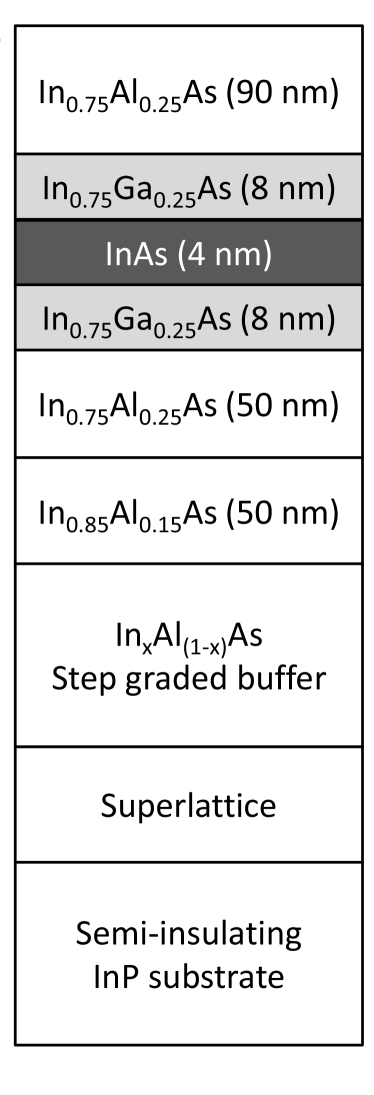
We used an InAs QW grown by molecular beam epitaxy with the density and the mobility . The 2DEG is formed in the 4 nm-thick InAs layer. The material stack of the InAs heterostructure is schematically shown in Fig. 4. A mesa was first defined in the substrate by wet etching with an etchant based on . Then, NbTi was sputtered to form the superconducting electrodes on the mesa edges, following a procedure of wet etching to make the clean edge exposed, sulfur passivation to avoid oxidization of the edge, and in-situ Ar plasma cleaning. Finally a gate electrode metal of Titanium and Gold was deposited on top to address the low QH filling regime even under a low magnetic field. The top gate is placed on an insulating layer made from cross-linked PMMA. This fabrication procedure creates no superconducting material on the top surface of the mesa. This is specially devised to control the carrier density not only of the mesa but also near the junction using the top gate voltage (discussed later). The two junctions are separated by 20 m, so this device is assumed to have two independent contact regions.
.2 NbTi superconductivity
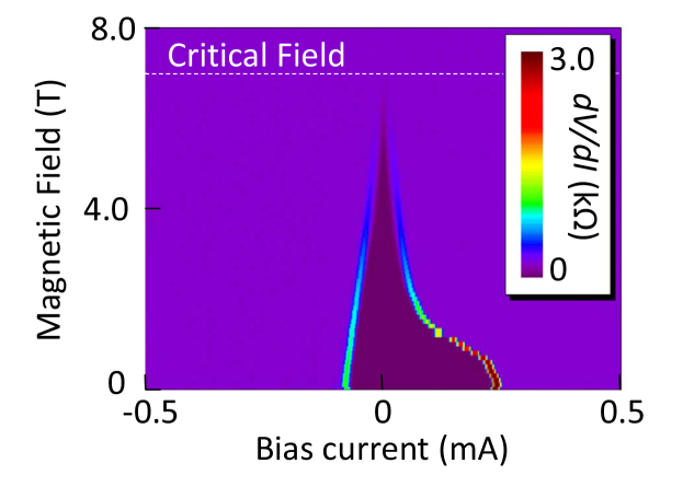
To characterize the superconducting properties of the NbTi, we performed a current-bias measurement of the differential resistance at various out-of-plane magnetic fields for a 150 nm-thick NbTi thin film device at 2 K which is lower than the NbTi critical temperature of 6.5 K. The measured data shows a supercurrent branch as =0 k in dark purple near the zero current bias in Fig. 5. From this data, we evaluate the critical field of 7.0 T. Herein, the coexistence of superconducting state and QH states can be realized if the 2DEG is in the spin-resolved QH regime for T.
.3 Superconducting proximity at 0 T
In Fig. 2(a) and (c) in the main text, there are dip structures around mV. These dip structures cannot be expected from the normal BTK model. These dip structures have also been reported in experimental studies of junctions of three dimensional topological insulators and superconductor Snelder et al. (2015). Some theoretical works predict existence of spin-triplet superconducting proximity on such junctions which generate the dip structures Burset et al. (2014, 2015). In our case, strong spin-orbit interaction on the interface can affect the superconducting proximity even at 0 T and invokes finite spin-flip process. Therefore, we suspect that the dip structure may be related to the spin-triplet superconducting proximity even at 0 T.
.4 Transconductance in the QH regime
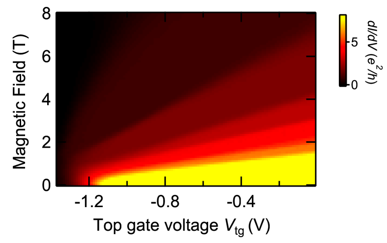
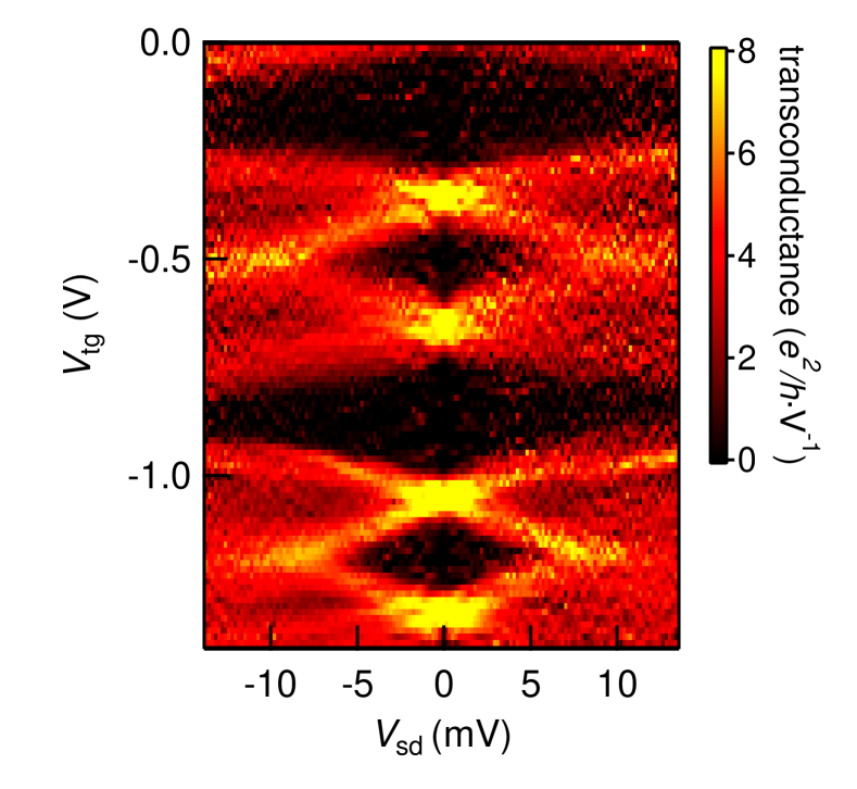
We measured the conductance as functions of magnetic field and top gate voltage in order to estimate quality of our InAs quantum Hall effect and Zeeman effect. Figure 6 shows the conductance as functions of and . As seen in this figure, clear quantized conductance plateaus appear at T and the Zeeman splitting is found at T. 2.4 and 4 T is large enough to study the coexistence between the spin-resolved QH state and superconductor. Furthermore, we measured the transconductance defined by the deviation of at 2.4 T. The results are plotted in Fig. 7. The diamond-shaped structure can be found. We focus on the bright areas, namely the plateau-transition regime in the main text.
.5 Sub-gap feature in QH plateau regime
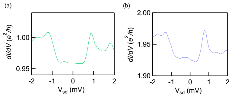
In the main text, we focus on the sub-gap feature in QH plateau-transition regime. In this section, we show the measured vs in the plateau regime. The typical results obtained at 4 T are shown in Fig. 8. Panel (a) and (b) indicates the result on the and 2 plateau, respectively. Even in the plateau regime, there is a sub-gap feature with a small dip or gap-like structure. These results are similar to the sub-gap features observed for of Fig. 3(b) and (c) in the main text. The estimated gap from these sub-gap features are nearly equal to the 0.35 mV calculated from the superconducting gap at 0 T. This supports our assumption in the main text that the spin-singlet superconducting proximity gap at 4 T is the same as the superconducting gap obtained at 0 T. We conclude that the QH edge states don’t contribute to the Andreev reflection in the device.
.6 Numerical calculation
We executed the numerical calculation using the model in which we assume the two channels, and . The fitting parameters are the superconducting gaps and , barrier strength (), normal state interface conductance , effective temperature , the relative contribution of channel , and offset conductance . We define as eqn. (2) in the main text. Then the fitting function can be written as
We take care to confirm that our device has two independent superconducting-QH bulk state junctions. Therefore, the sub-gap features and the position in of the side peaks are consistent with and . To account for the effective temperature, we approximated the deviation of the Fermi-Dirac distribution function in eqn. (1) in the main text as the Gaussian function, , where is ideally equal to but now includes the broadening due to inelastic scattering, inhomogeneity of the gap and the local heating Woods et al. (2004); DeGrave et al. (2011). To execute the fitting, we constrict the fitting ranges for all the parameters, and especially we tightly constrict the and from the curve shapes. In order to reproduce the curve shape around the zero bias voltage, we changed the fitting range for each of the curves because the differential conductance of the 2DEG appears as background and the conductance has a large dependence on the bias voltage near the plateau regime. Due to this background dependence, we could not reproduce the curve shapes in the two lower curves of the left panel and middle panel, and the lowest curve of the right panel in Fig.4(b) of the main text. In these cases, we evaluated only and from the sub-gap peak features ( and are indicated on the panels in Fig.4(b) as open and closed hexagons). Our fitting scheme includes many free parameters and results are sensitive to the constriction of the variable range. However, the estimated gap energies and produce relatively constant results with different fitting ranges, so we think it is valuable to discuss these parameters. All fits are executed with a genetic algorithm (GenCurvefit package for Igor Pro).
.7 Calculation of the proximity gap energy
As written in the main text, we analyzed our experimental data with the model to evaluate and , the superconducting gap energies. However, these values are enlarged from the true bulk and proximity superconducting gap energies due to dissipation induced from the bulk state of the mesa. In the plateau regime, the transport is non-dissipative in the mesa, while the transport is dissipative in the plateau-transition regime due to the QH bulk state. Herein, in the plateau-transition regime, applied between two superconductors is divided into the voltage on the junctions and on the mesa, then the deduced gives a larger gap energy as the contribution of the QH bulk state in the transport becomes larger. The equivalent circuit is represented in Fig. 2(d) in the main text. Consequently, produces a peak in the middle of the plateau-transition regime where the bulk contribution becomes maximum. The true bulk superconducting gap energies (corresponding to the gap for channel ), meV, can be evaluated from near the plateau regime. From this gap energy, we calculated the true superconducting proximity gap energy, meV as . The calculated gap, as a function of , at mV in unit of is shown in Fig.9.
.8 The maximum position of the bulk contribution
Our results for and have a maximum and minimum, respectively, at . In this section, we estimate how large should be to make the bulk contribution have a maximum at .
As the shape of our device is square, the two-terminal conductance is written by . and are the longitudinal conductivity and Hall conductivity Lippmann and Kuhrt (1958); Jensen and Smith (1972); Abanin and Levitov (2008), respectively. has a maximum when the bulk contribution is maximum and the situation is given by (), at which change in the filling factor is equal to 0.5. Herein, if the bulk contribution is maximum at (namely ), should be 0.49 (0.5), 0.80 (1.5), and 1.02 (2.5) in the cases, respectively. From these conductivity, we can calculate the longitudinal resistance,, resulting in 1.0 (), 0.28(), and 0.14() in the cases, respectively. The calculated longitudinal resistance should be obtained when the bulk contribution is maximum, meaning is maximum with the calculated resistance in the region corresponding to the plateau-transition regime. We measured a Hall bar device at 2 K, fabricated from the same InAs quantum well wafer as we used for the superconducting devices and the results are shown in Fig. 10. has some peaks consistent with the finite bulk contribution. The maximum of at 4 T is at 4 k and 1.5 k corresponding to the cases, respectively. The measured resistances are comparable to the estimated resistance based on the assumption that the bulk contribution is maximum at ().
References
- Andreev (1964) A. F. Andreev, Sov. Phys. JETP. 19, 1228 (1964).
- Bergeret et al. (2005) F. S. Bergeret, A. F. Volkov, and K. B. Efetov, Rev. Mod. Phys. 77, 1321 (2005).
- Keizer et al. (2010) R. S. Keizer, S. T. B. Goennenwein, T. M. Klapwijk, G. Miao, G. Xiao, and A. Gupta, Nature 439, 825 (2010).
- Asano et al. (2007a) Y. Asano, Y. Tanaka, and A. A. Golubov, Phys. Rev. Lett. 98, 107002 (2007a).
- Asano et al. (2007b) Y. Asano, Y. Sawa, Y. Tanaka, and A. A. Golubov, Phys. Rev. B 76, 224525 (2007b).
- Robinson et al. (2010) J. W. A. Robinson, J. D. S. Witt, and M. G. Blamire, Science 329, 59 (2010).
- Visani et al. (2012) C. Visani, Z. Sefrioui, J. Tornos, C. Leon, J. Briatico, M. Bibes, A. Barthelemy, J. Santamaria, and J. E. Villegas, Nature Physics 8, 539 (2012).
- Linder and Robinson (2015) J. Linder and J. W. A. Robinson, Nature Physics 11, 307 (2015).
- Eschrig and Lofwander (2008) M. Eschrig and T. Lofwander, Nature Physics 4, 138 (2008).
- van Ostaay et al. (2011) J. A. M. van Ostaay, A. R. Akhmerov, and C. W. J. Beenakker, Phys. Rev. B 83, 195441 (2011).
- Luo et al. (1988) J. Luo, H. Munekata, F. F. Fang, and P. J. Stiles, Phys. Rev. B 38, 10142 (1988).
- de Andrada e Silva et al. (1997) E. A. de Andrada e Silva, G. C. La Rocca, and F. Bassani, Phys. Rev. B 55, 16293 (1997).
- Nitta et al. (1997) J. Nitta, T. Akazaki, H. Takayanagi, and T. Enoki, Phys. Rev. Lett. 78, 1335 (1997).
- Heida et al. (1998) J. P. Heida, B. J. van Wees, J. J. Kuipers, T. M. Klapwijk, and G. Borghs, Phys. Rev. B 57, 11911 (1998).
- Takayanagi and Akazaki (1998) H. Takayanagi and T. Akazaki, Physica B: Condensed Matter 249-251, 462 (1998).
- Eroms et al. (2005) J. Eroms, D. Weiss, J. D. Boeck, G. Borghs, and U. Zülicke, Phys. Rev. Lett. 95, 107001 (2005).
- Rickhaus et al. (2012) P. Rickhaus, M. Weiss, L. Marot, and C. Schonenberger, Nano Letters 12, 1942 (2012), pMID: 22417183.
- Komatsu et al. (2012) K. Komatsu, C. Li, S. Autier-Laurent, H. Bouchiat, and S. Guéron, Phys. Rev. B 86, 115412 (2012).
- Wan et al. (2015) Z. Wan, A. Kazakov, M. J. Manfra, L. N. Pfeiffer, K. W. West, and L. P. Rokhinson, Nature Communications 6, 7426 (2015).
- Amet et al. (2016) F. Amet, C. T. Ke, I. V. Borzenets, J. Wang, K. Watanabe, T. Taniguchi, R. S. Deacon, M. Yamamoto, Y. Bomze, S. Tarucha, and G. Finkelstein, Science 352, 966 (2016).
- Qi et al. (2010) X.-L. Qi, T. L. Hughes, and S.-C. Zhang, Phys. Rev. B 82, 184516 (2010).
- Fu and Kane (2008) L. Fu and C. L. Kane, Phys. Rev. Lett. 100, 096407 (2008).
- Hasan and Kane (2010) M. Z. Hasan and C. L. Kane, Rev. Mod. Phys. 82, 3045 (2010).
- Mourik et al. (2012) V. Mourik, K. Zuo, S. M. Frolov, S. R. Plissard, E. P. A. M. Bakkers, and L. P. Kouwenhoven, Science 336, 1003 (2012).
- Das et al. (2012) A. Das, Y. Ronen, Y. Most, Y. Oreg, M. Heiblum, and H. Shtrikman, Nature Physics 8, 887 (2012).
- Rokhinson et al. (2012) L. P. Rokhinson, X. Liu, and J. K. Furdyna, Nature Physics 8, 795 (2012).
- Nadj-Perge et al. (2014) S. Nadj-Perge, I. K. Drozdov, J. Li, H. Chen, S. Jeon, J. Seo, A. H. MacDonald, B. A. Bernevig, and A. Yazdani, Science 346, 602 (2014).
- Bocquillon et al. (2016) E. Bocquillon, R. S. Deacon, J. Wiedenmann, P. Leubner, T. M. Klapwijk, C. Brune, K. Ishibashi, H. Buhmann, and L. W. Molenkamp, Nature Nanotechnology 12, 137 (2016).
- Wiedenmann et al. (2016) J. Wiedenmann, E. Bocquillon, R. S. Deacon, S. Hartinger, O. Herrmann, T. M. Klapwijk, L. Maier, C. Ames, C. Brune, C. Gould, A. Oiwa, K. Ishibashi, S. Tarucha, H. Buhmann, and L. W. Molenkamp, Nature Communications 7, 10303 (2016).
- Albrecht et al. (2016) S. M. Albrecht, A. P. Higginbotham, M. Madsen, F. Kuemmeth, T. S. Jespersen, J. Nygard, P. Krogstrup, and C. M. Marcus, Nature 531, 206 (2016).
- Deacon et al. (2016) R. S. Deacon, J. Wiedenmann, E. Bocquillon, F. Dominguez, T. M. Klapwijk, P. Leubner, C. Brune, E. M. Hankiewicz, S. Tarucha, K. Ishibashi, H. Buhmann, and L. W. Molenkamp, arXiv , 1603.09611 (2016).
- Shabani et al. (2014a) J. Shabani, S. Das Sarma, and C. J. Palmstrøm, Phys. Rev. B 90, 161303 (2014a).
- Shabani et al. (2014b) J. Shabani, A. P. McFadden, B. Shojaei, and C. J. Palmstrøm, Applied Physics Letters 105, 262105 (2014b).
- Blonder et al. (1982) G. E. Blonder, M. Tinkham, and T. M. Klapwijk, Phys. Rev. B 25, 4515 (1982).
- Irie et al. (2016) H. Irie, C. Todt, N. Kumada, Y. Harada, H. Sugiyama, T. Akazaki, and K. Muraki, Phys. Rev. B 94, 155305 (2016).
- Tang et al. (1996) H. X. Tang, Z. D. Wang, and Y. Zhang, Z. Phys. B 101, 359 (1996).
- Burset et al. (2014) P. Burset, F. Keidel, Y. Tanaka, N. Nagaosa, and B. Trauzettel, Phys. Rev. B 90, 085438 (2014).
- Burset et al. (2015) P. Burset, B. Lu, G. Tkachov, Y. Tanaka, E. M. Hankiewicz, and B. Trauzettel, Phys. Rev. B 92, 205424 (2015).
- Hoppe et al. (2000) H. Hoppe, U. Zülicke, and G. Schön, Phys. Rev. Lett. 84, 1804 (2000).
- Giazotto et al. (2005) F. Giazotto, M. Governale, U. Zülicke, and F. Beltram, Phys. Rev. B 72, 054518 (2005).
- Khaymovich et al. (2010) I. M. Khaymovich, N. M. Chtchelkatchev, I. A. Shereshevskii, and A. S. Mel’nikov, EPL (Europhysics Letters) 91, 17005 (2010).
- Snelder et al. (2015) M. Snelder, M. P. Stehno, A. A. Golubov, C. G. Molenaar, T. Scholten, D. Wu, Y. K. Huang, W. G. van der Wiel, M. S. Golden, and A. Brinkman, arXiv 1506, 05923 (2015).
- Woods et al. (2004) G. T. Woods, R. J. Soulen, I. Mazin, B. Nadgorny, M. S. Osofsky, J. Sanders, H. Srikanth, W. F. Egelhoff, and R. Datla, Phys. Rev. B 70, 054416 (2004).
- DeGrave et al. (2011) J. P. DeGrave, A. L. Schmitt, R. S. Selinsky, J. M. Higgins, D. J. Keavney, and S. Jin, Nano Letters 11, 4431 (2011), pMID: 21923114, http://dx.doi.org/10.1021/nl2026426 .
- Lippmann and Kuhrt (1958) H. J. Lippmann and R. Kuhrt, Z. Naturforsch. A 13, 462 (1958).
- Jensen and Smith (1972) H. H. Jensen and H. Smith, Journal of Physics C: Solid State Physics 5, 2867 (1972).
- Abanin and Levitov (2008) D. A. Abanin and L. S. Levitov, Phys. Rev. B 78, 035416 (2008).