Amorphous to amorphous insulator-metal transition in GeSe3:Ag glasses
Abstract
We study an insulator-metal transition in a ternary chalcogenide glass (GeSe3)1-xAgx for =0.15 and 0.25. The conducting phase of the glass is obtained by using “Gap Sculpting” (Prasai et al, Sci. Rep. 5:15522 (2015)) and it is observed that the metallic and insulating phases have nearly identical DFT energies but have a conductivity contrast of . The transition from insulator to metal involves growth of an Ag-rich phase accompanied by a depletion of tetrahedrally bonded Ge(Se1/2)4 in the host network. The relative fraction of the amorphous Ag2Se phase and GeSe2 phase is shown to be a critical determinant of DC conductivity.
pacs:
Valid PACS appear hereMetal-Insulator transitions (MIT) and their associated science are among the cornerstones of condensed matter physics Mott and Davis (2012). In this Letter, we describe the atomistics of a technically important but poorly understood MIT in GeSe:Ag glasses, a prime workhorse of conducting bridge memory (CBRAM) devices Kozicki and Mitkova (2003); Valov et al. (2011). By design, we construct a stable conducting model from a slightly favored insulating phase. Predictions are made for structural, electronic and transport properties. We demonstrate the utility of our “Gap sculpting” method Prasai et al. (2015) as a tool of Materials Design.
We report metallic phases of amorphous (GeSe3)1-xAgx at and . These are canonical examples of Ag-doped chalcogenide glasses, which are studied in relation to their photo-response and diverse opto-electronic applications Kolobov (2006); Mitkova . Ag is remarkably mobile making the material a solid electrolyte and is known to act as “network-modifier” in these glasses and alter the connectivity of network. Experiments have shown Se rich ternaries ((GeySe1-y)1-xAgx with y ) to be phase-separated into Ag-rich Ag2Se phase and residual GetSe1-t phase Mitkova et al. (1999).
Using first-principles calculations, we show that stable amorphous phases with at least times higher electronic conductivity exist with only small ( eV/atom) difference in total energy. These conducting states present the same basic structural order in the glass, but have a higher relative fraction of an a-Ag2Se phase compared to the insulating states. It is known that amorphous materials are characterized by large numbers of degenerate conformations that are mutually accessible to each other at small energy cost, but those usually have identical macroscopic properties. The remarkable utility of these materials accrues from states with distinct properties, nevertheless readily accessible to each other.
We discover the conducting phase of GeSe3Ag glass by designing atomistic models with a large density of states (DOS) near the Fermi energy Prasai et al. (2015). This is achieved by utilizing Hellmann-Feynman forces from the band edge states. These forces are used to bias the true forces in ab initio molecular dynamics (AIMD) simulations to form structures with a large DOS at the Fermi level. The biased force on atom , , is obtained by suitably summing Hellmann Feynman forces for the band edge states (second term in Eq. 1) with the total force from AIMD calculations, .
| (1) |
Here, ’s set the sign and magnitude of the HF forces from individual states i. To maximize the density of states near , gap states closer to the valence edge will have , whereas the states in the conduction edge will have . The magnitude of determines the size of biasing force (with representing true AIMD forces). We have employed biased forces as an electronic constraint to model semiconductors and insulators in our recently published work Prasai et al. (2016a) where the biasing is done in just the opposite sense: to force to states out of the band gap region.
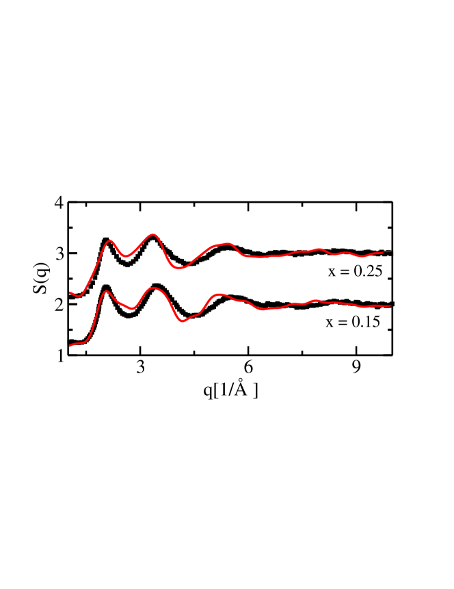
We start with conventional 240 atom models of (GeSe3)1-xAgx, =0.15 and 0.25, at their experimental densities 5.03 and 5.31 gm/cm3 Piarristeguy et al. (2000) respectively. These were prepared using melt-quench MD simulations, followed by conjugate-gradient relaxation to a local energy minimum. The MD simulations are performed using the Vienna Ab initio Simulation Package (VASP) Kresse and Furthmüller (1996a); *kresse2. Plane waves of up to 350 eV are used as basis and DFT exchange correlation functionals of Perdew-Burke-Ernzerhof Perdew et al. (1996) were used. Brillouin zone (BZ) is represented by -point for bulk of the calculations. For static calculations, BZ is sampled over 4 k-points. These models fit the experimental structure factor reasonably well (Figure 1).
We obtain conducting conformations by annealing the starting configurations using biased forces at 700 K for 18 ps. The electronic states in the energy range [–0.4 eV, +0.4 eV] are included in the computation of bias force and is used. The bias potential () shepherds the electronic states in the band edges into the band-gap region. Since we want any proposed metallic conformation to be a true minimum of the unbiased DFT energy functional, we relax instantaneous snapshots of biased dynamics (taken at the interval of 0.2 ps, leaving out the first 4 ps) to their nearest minima using conjugate gradient algorithm with true DFT-GGA forces. We study all relaxed snapshots by i) gauging the density and localization of states around Fermi energy and, ii) testing the stability of the configurations by annealing them at 300 K (n.b. glass transition temperatures () are 488 K and 496 K for compositions =0.15 and 0.25 respectively Arcondo et al. (2007)). At each composition, we selected five models that display a large density of extended states around Fermi energy and are stable against extended annealing at 300 K as the ‘metallized’ models. These metallized systems are, on average, 0.0400.009 eV/atom above their insulating counterparts.
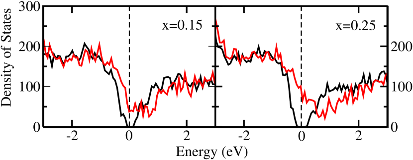
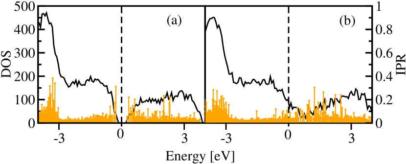
The metallized models, by construction, show a large density of states around Fermi energy (Fig. 2) whereas the insulating models display small but well defined PBE gap of 0.41 eV and 0.54 eV for =0.15 and 0.25 respectively. For disordered materials, a high DOS at alone may not produce conducting behaviour since these states can be localized (example: amorphous graphene, Van Tuan et al. (2012)). We gauge the localization of these states by computing inverse participation ratio (IPR, Ziman (1979))(plotted for =0.25 system in Figure 3) and show that these states are indeed extended. We compute the electronic conductivity [] using Kubo-Greenwood formula (KGF) in the following form:
| (2) | |||
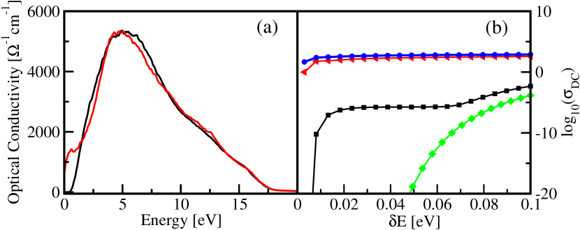
It has been used with reasonable success to predict conductivity Abtew et al. (2007); *galli1990; *allen1987. Our calculations used 4 k-points to sample the Brillouin zone. To compensate for the sparseness in the DOS due to the size of the supercell, a Gaussian broadening (E) for the -function is used. We note that the choice of E between 0.01 eV and 0.1 eV does not significantly alter the computed values of DC conductivity [] (Figure 4). For the choice of E=0.05 eV (which is small compared to the thermal fluctuation of Kohn-Sham states for disordered systems at room temperature. For a heuristic theory, see Prasai et al. (2016b)), the DC conductivity of metallic models are of the order of at both concentrations. For the insulating model at =0.15, this value is of order whereas for insulating model at =0.25, this value is lower but can not be ascertained from our calculations. We find that the metallized models show, at least, times higher conductivity than the insulating models. The computed conductivity for metallic models are comparable to the DC conductivity values of liquid silicon (, Glazov et al. (1969)).
We track the atomic rearrangements associated with the metallization of network to identify the microscopic origin of metallicity. Recalling that these are inhomogenous glasses with phase separation into Ag-rich a-Ag2Se phase and residual Ge-Se backbone, we note that the insulator-metal transition in these glasses can be viewed in terms of relative ratio of these two competing phases. In particular, we make the following three observations associated with the insulator-metal transition: i) Growth of Ag-Se phase, ii) Depletion of tetrahedral GeSe2 phase, and iii) Growth of Ge-rich phase in host network. Below we briefly comment on these three observations, a more detailed account of structural rearrangements will be published later.
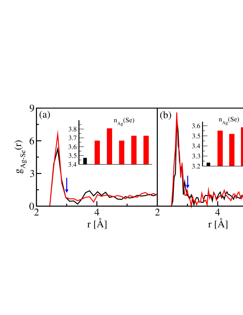
Growth of Ag-Se phase. We observe that the Ag-Se phase grows upon metallization. Se-Ag correlation ( Å) is found to increase from the insulating to metallic model (see Figure 5, also the increase in peak P2 in Figure 6). For both Ag concentrations, Se-coordination around Ag is found to increase from insulating to metallic models. For =0.15, Se-coordination around Ag increases from 3.47 to 3.72 (the later value is an average over 5 metallic models, see Figure 5). For =0.25, it increases from 3.23 to (on average) 3.53.
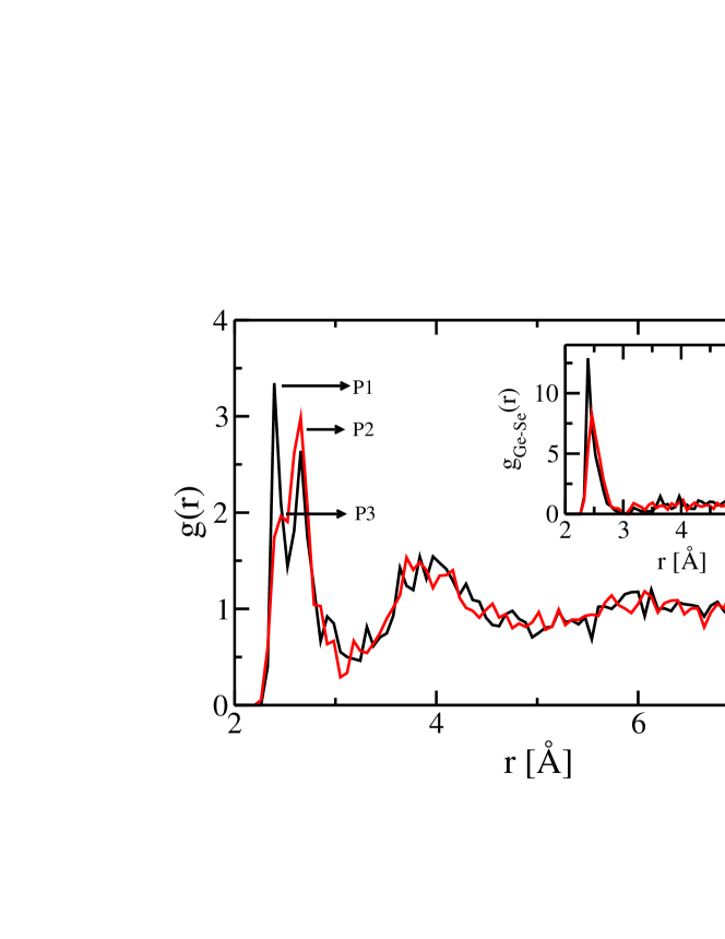
Depletion of tetrahedral GeSe2. The network in the insulating phase is dominated by Se-rich tetrahedral Ge(Se1/2)4, accompanied by a competing Ag-Se phase. The fraction of later phase is directly determined by Ag-concentration in the network. These two phases appear as two distinct peaks in total radial distribution function (RDF) (Figure 6). Upon metallization, the growth of Ag-Se shifts the balance of stoichiometries in network and the host network becomes Se deficient. At composition =0.25 (plotted in Fig. 6), the network in metallic phase is dominated by the Ag-Se subnetwork (peak P2). The corresponding Ge-Se coordination number in metallic model is 3.22, slightly lower than 3.40 in insulating model. These values are 3.28 and 3.43 respectively for =0.15. The correlation cutoff of 2.70 Å is taken to determine the coordinations.
Response of host network. The host network of Ge-Se consists of Se-rich tetrahedral GeSe2 and non-tetrahedral Ge-rich phases including the ethane-like Ge2Se3 units. These subnetworks were reported in GeSe2 by Boolchand and coworkers Boolchand and Bresser (2000) and in ternary chalcogenide glasses by Mitkova and coworkers Mitkova et al. (2006). We find that these Ge-Se stoichiometries have different bondlength distributions: Se rich phases () have bondlengths smaller than 2.55 Å whereas Ge-rich phases () have bondlengths longer than 2.55 Å. In an insulating conformation, the former phase dominates and registers an RDF peak at 2.40 Å (Fig. 6). For metallic conformations, fewer Se atoms are available to Ge. This increases the fraction of Ge-rich phases and the Ge-Se bondlength distribution shifts to longer distances. This is represented by a shift in Ge-Se pair correlation function in Figure 6 (inset) and appearence of peak P3 in total RDF. Due to increase in fraction of Ge2(Se1/2)6, Ge-Ge correlation peak appears around 3.5 Å in metallic models. We note that it is such a Ge-Ge signal in Raman scattering and 119Sn Mssbauer spectroscopy that led to experimental discovery of Ge-rich Ge2(Se1/2)6 phase in stoichiometric bulk GexSe100-x glasses Boolchand and Bresser (2000).
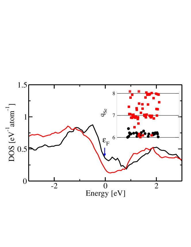
Now we comment further on the role of Ag-Se phase in metallicity. It is well known that the states around Fermi energy are mainly Se p-orbitals (Prasai and Drabold (2011); Tafen et al. (2005), In GeSAg: Akola et al. (2015)). The electronic structure of metallic model projected onto its constituent subnetworks (Ag-Se and Ge-Se) shows different electronic activity of Se-atoms in the two subnetworks. We find that individual Se atoms in Ag2Se nework have twice as much projection around the Fermi energy than the Se atoms in Ge-Se network (Figure 7). This suggests that a more concentrated Ag-Se network will enhance the conduction. Experimentally, growth of Ag-rich nanocrystals in GeS2 matrix has been shown to enhance the electronic conductivity Wang et al. (2012); *waser2009. The Se-atoms in Ag-Se phase are found in atomic state () where as those in Ge-Se network are ionic with negative charge ( or ) (See inset in Figure 7).
Altogether, we have presented a direct simulation of conducting phase of CBRAM material GeSe3Ag and it provides evidence of the conduction through interconnected regions of Ag2Se phase in the glassy matrix Wang et al. (2012); *waser2009. This work does not attempt to describe the conduction through Ag-nanowires which may be the mechanism of conduction in two terminal metal-electrolyte-metal devices Kozicki et al. (2015). It demonstrates the existence of metastable amorphous forms (“poly-amorphism”) of the glass with drastically different optical response. The observation that the DFT energies of these states are only 0.04 eV/atom higher than insulating state suggests that these states might to accessible. Furthermore, we have shown that “Gap Sculpting” can be used to purposefully design metallic conformation.
We thank M. Mitkova and P. Boolchand for stimulating discussions. This work is supported by National Science Foundation under grant no. DMR 1506836, no. DMR 1507670 and no. DMR 1507166. We are thankful to Ohio Supercomputer center for computing resources.
References
- Mott and Davis (2012) N. F. Mott and E. A. Davis, Electronic processes in non-crystalline materials (OUP Oxford, 2012).
- Kozicki and Mitkova (2003) M. N. Kozicki and M. Mitkova, “Microelectronic programmable device and methods of forming and programming the same,” (2003), uS Patent 6,635,914.
- Valov et al. (2011) I. Valov et al., Nanotechnology 22, 254003 (2011).
- Prasai et al. (2015) K. Prasai et al., Scientific Reports 5 (2015).
- Kolobov (2006) A. V. Kolobov, ed., Photo-induced metastability in amorphous semiconductors (John Wiley & Sons, 2006).
- (6) M. Mitkova, “Real time optical recording on thin films of amorphous semiconductors,” in Insulating and semiconducting glasses, edited by P. Boolchand (World Scientific).
- Mitkova et al. (1999) M. Mitkova et al., Physical Review Letters 83, 3848 (1999).
- Prasai et al. (2016a) K. Prasai et al., Physica Status Solidi (a) 213, 1653 (2016a).
- Piarristeguy et al. (2000) A. Piarristeguy et al., Journal of Non-Crystalline solids 273, 30 (2000).
- Kresse and Furthmüller (1996a) G. Kresse and J. Furthmüller, Physical Review B 54, 11169 (1996a).
- Kresse and Furthmüller (1996b) G. Kresse and J. Furthmüller, Computational Materials Science 6, 15 (1996b).
- Perdew et al. (1996) J. P. Perdew et al., Physical Review Letters 77, 3865 (1996).
- Arcondo et al. (2007) B. Arcondo et al., Physica B: Condensed Matter 389, 77 (2007).
- Van Tuan et al. (2012) D. Van Tuan et al., Physical Review B 86, 121408 (2012).
- Ziman (1979) J. M. Ziman, Models of disorder: the theoretical physics of homogeneously disordered systems (CUP Archive, 1979).
- Abtew et al. (2007) T. Abtew et al., Physical Review B 76, 045212 (2007).
- Galli et al. (1990) G. Galli et al., Physical Review B 42, 7470 (1990).
- Allen and Broughton (1987) P. B. Allen and J. Q. Broughton, J. Phys. Chem.;(United States) 91 (1987).
- Prasai et al. (2016b) K. Prasai et al., Semiconductor Science and Technology 31, 73002 (2016b).
- Glazov et al. (1969) V. M. Glazov et al., Plenum Press, New York, 1969, 362 P (1969).
- Boolchand and Bresser (2000) P. Boolchand and W. Bresser, Philosophical Magazine B 80, 1757 (2000).
- Mitkova et al. (2006) M. Mitkova et al., Journal of Non-Crystalline solids 352, 1986 (2006).
- Prasai and Drabold (2011) B. Prasai and D. Drabold, Physical Review B 83, 094202 (2011).
- Tafen et al. (2005) D. N. Tafen et al., Physical Review B 72, 054206 (2005).
- Akola et al. (2015) J. Akola et al., Journal of Physics: Condensed Matter 27, 485304 (2015).
- Wang et al. (2012) R. Y. Wang et al., Advanced Materials 24, 99 (2012).
- Waser et al. (2009) R. Waser et al., Advanced Materials 21, 2632 (2009).
- Kozicki et al. (2015) M. N. Kozicki et al., “Electrochemical metallization memories,” in Resistive Switching: From Fundamentals of Nanoionic Redox Processes to Memristive Device Applications, edited by D. Ielmini and R. Waser (John Wiley & Sons, 2015) pp. 483–514.