Probing the Quantum States of a Single Atom Transistor at Microwave Frequencies
Abstract
The ability to apply GHz frequencies to control the quantum state of a single atom is an essential requirement for the fast gate pulsing needed for qubit control in donor based silicon quantum computation. Here we demonstrate this with nanosecond accuracy in an all epitaxial single atom transistor by applying excitation signals at frequencies up to 13 GHz to heavily phosphorous doped silicon leads. These measurements allow the differentiation between the excited states of the single atom and the density of states in the one dimensional leads. Our pulse spectroscopy experiments confirm the presence of an excited state at an energy 9 meV consistent with the first excited state of a single donor in silicon. The relaxation rate of this first excited state to ground is estimated to be larger than 2.5 GHz, consistent with theoretical predictions. These results represent a systematic investigation of how an atomically precise single atom transistor device behaves under rf excitations.
Advances in Si device fabrication technology over the past decade have driven the scale of transistors down to the atomic level. The ultimate limit of this scaling is to fabricate a transistor with just one single dopant atom as the active component of the device and this has been realised using scanning tunnelling microscope (STM) lithography. Sch136104 The spin states of individual P donor electrons and nuclei have extremely long coherence times when incorporated into a crystal composed of isotopically purified 28Si, Tyr2012 ; Ste2012 ; Muh2014 making them excellent candidates for quantum information processing applications. Kane133 ; Loss120 ; Pla2012 STM lithography offers the potential to scale up such qubits by providing a means to position individual P atoms in a Si lattice, and align them with sub-nanometer precision to monolayer doped control electrodes. This technique has already demonstrated double Web4001 and triple Wat1830 quantum dot devices, controllable exchange interactions between electrons, Web430 and the ability to initialise and read out the spin states of single electrons bound to the donor with extremely high fidelity. Wat2015 Most recently, these monolayer doped gates have shown to be immune to background charge fluctuations making them excellent interconnects for silicon based quantum computer. Sha233304 ; Sha236602 ; Sha3
Besides the ability to create devices with atomic precision, another requirement for quantum information processing and high-speed logic applications is the ability to control the quantum states of the donor electrons at sub nanosecond timescales. Control signals in the GHz regime are desirable for dispersive readout Hou15 and for controlling exchange interactions for non-adiabatic gate operations Pet2180 . Indeed, a recently proposed scheme for implementing the surface-code error correction protocol in silicon relies on the ability to propagate signals through such devices with sub-nanosecond timing precision. Hill15 Recent impurity-based quantum charge pump devices have been shown to be robust in terms of immunity to pumping errors when operated at GHz frequencies. Tet063036 ; Fuj207 However, to date these experiments have been performed on devices containing random ion implanted impurities. Tet063036 ; Fuj207 STM fabrication capabilities can allow high-precision ( nm) positioning of the dopant Sch136104 , and when combined with high-speed control of quantum states, it will provide devices for quantum metrology. Tet063036 ; Fuj207
In this paper we investigate the propagation of high-frequency signals to the monolayer-doped leads used in atomically precise devices. Previous results have demonstrated the ability to apply radio frequency ( MHz) transmission using dispersive measurements for manipulation of the quantum states. Hou15 Here we present a systematic study of the propagation of high frequency signals in atomically precise devices. In this work we demonstrate high frequency capacitive coupling (up to 13 GHz) to the states of a single-atom transistor Fue242 ; Fue2011 fabricated via scanning tunnelling microscope lithography, see Fig. 1a), important for the implementation of quantum information processing Tyr2012 ; Ste2012 ; Muh2014 ; Kane133 ; Loss120 ; Pla2012 ; Hill15 and quantum metrology. Tet063036 ; Fuj207 We report transient spectroscopy experiments Fuj081304 ; Volk1753 that confirm the existence of the excited state of the P donor located at an energy of 9 meV 1 meV and we extract bounds from 2.5 GHz to 162 GHz for the relaxation rates from the first excited state to the ground state, , i.e. in good agreement with previous experiments Zhu093104 ; HubS211 and theoretical estimations. Tah075302 It is important to note that such a large range in the extracted value of can be linked to the strong tunnel coupling of the state to source/drain leads in this particular device, making the experiments needed for a more quantitative result infeasible. Fuj081304 ; Volk1753 However, in the long term this coupling can be controlled by the geometry of the tunnel junctions, which can be engineered with sub-nm precision during fabrication. Cam2013
RESULTS AND DISCUSSION
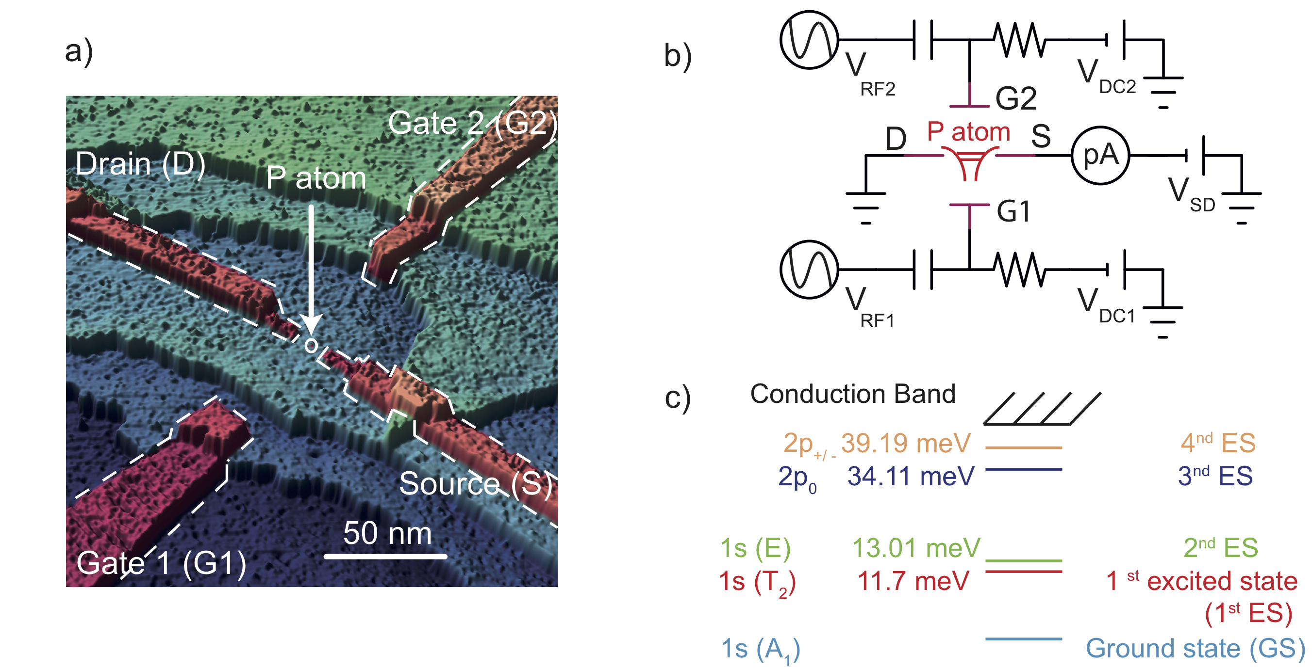
In contrast to surface gate-defined quantum dot devices, which typically make use of macroscopic metal electrodes to propagate high-frequency signals, atomic precision devices rely on electrodes formed using highly phosphorus doped silicon ( 2.5 ) where the phosphorus dopants form a monatomic layer within the Si crystal patterned in the same lithographic step as the single donor atom, see Fig. 1 a). Within the monolayer of dopants the average separation of the donors is 1 nm giving rise to a highly disordered two-dimensional electron gas. Disorder scattering in these degenerately doped leads gives rise to a resistance of hundreds Ohms per square comparable to that found in silicon quantum dots Zwa961 but one order of magniture higher than the values observed in conventional transistors. Kei7080 However, another very important difference is that the self-capacitance of the atomically thin monolayer wires are negligible with the cross capacitances to the other leads being quite small, estimated to be around the aF Fue2011 . As a consequence, very little current ( nA) is required to carry a high-frequency voltage signal along these wires if compared to the tens of nA’s necessary for quantum dots. Zwa961
Fig. 1 shows in a) an STM image of the device and in b) a schematic of the measurement circuit used, illustrating how both dc and rf signals can be applied to gate 1 (G1) and to gate 2 (G2) via bias-tees. The pink areas in Fig. 1 a) show the highly doped monolayer regions (see also methods section) comprising tunnel coupled source/drain (S/D) leads and capacitively coupled gates (G1/G2) surrounding a single phosphorus atom. Several step edges separating the individual atomic planes are clearly visible in the STM image.
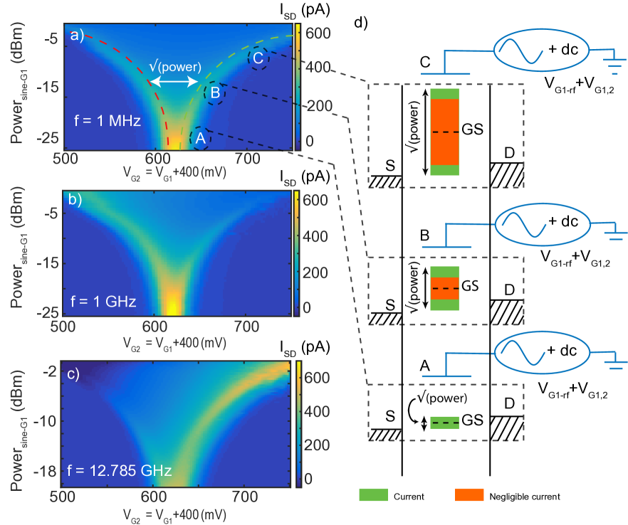
To test the frequency response of the monolayer doped gates, the to current peak related to current flow through the isolated atom Fue242 ; Fue2011 ; Tet063036 can be capacitively addressed by two gates (i.e. G1 and G2), allowing an independent rf signal to be added to each of the two gates and the device to be studied in both the dc and the rf domains. The use of rf signals is particularly attractive for these atomic-scale devices as the very narrow leads ( 5 nm) used to address the donor are quasi-1D, make it difficult, by using simple dc bias spectroscopy, to distinguish the signatures in current related to the excited states of the donor from the features related to the density of the states (DOS). Fue242 ; Fue2011 ; Ryu374 ; Mot161304 Later we will show how we apply transient current spectroscopy as described in Refs. Fuj081304 ; Volk1753 to clarify some of the transport mechanisms that can arise throughout the excited state spectrum of a single atom transistor. In Fig. 1 c) a schematic of the excitation spectrum of the state of a donor in Si Ram1297 is shown highlighting the 1s(), 1s() and 1s(E) valley states and the 2 and 2 orbital states of the single donor. In Fig. 2 we observe the evolution of the current peak related to the ground state (GS) of the state as a function of the power of the sinusoidal rf signal added to the dc voltage of gate 1. The possibility of capacitively addressing this GS is confirmed for high frequencies up to 13 GHz, where, as expected, when an rf signal with sufficient power is in use, the position of the current peak splits in two, with the splitting being proportional to the square root of the power of the provided excitation. This doubling of the current peak is observed for more than 4 orders of magnitude change in the frequency (i.e. from 1 MHz to 13 GHz). In Fig. 2d) we show a schematic describing how the doubling appears at different power and the underlying mechanisms causing it. When the rf signal is applied to one of the two gates (G1 or G2), during each rf cycle, the GS can occupy a range of positions represented by the green/red regions in the schematic of Fig. 2d) where the green and red regions simply refer to the voltage change rate at which the donor GS crosses the bias windows and depends on the timing of the sine wave (green = low rate of change of the sine; red = high rate of change of the sine).
To clarify, at any point in time of the sine period the current is proportional to the portion of integrated time that the states spend within the bias windows. Hence, if the variation in time of the position of the state is minimal (i.e. ), as in the green regions in Fig. 2d), it is possible for electrons to tunnel resonantly between the source and the drain via the state and it is possible to observe a current. However, if this variation in time is maximum (i.e. 1), as in the red regions, only negligible current can be observed.
In Fig. 3 we now turn to the impact of the rf on the response on the excited states of the donor atom. Fig. 3 a) shows the excited state spectrum at the to transition with no rf signal applied also consistent with previous measurements of this device. Fue242 ; Fue2011 ; Ryu374 In this figure the dc charge stability diagram focusses on the position of the first excited state, 1s (). Since we have the availability of two gates and the device is highly symmetric, the donor states can be capacitively addressed with both G1 and G2. As a consequence we can address the states in two different regimes either when G1 and G2 are tied together and varied simultaneously or when G1 is fixed and G2 is varied. By addressing the donor in those two different regimes we observe the same spectrum as in the original measurements Fue242 ; Fue2011 where, as expected, Rah165314 the positions of each level are insensitive to the changes in electric field related to the different measurement configurations, see Fig. 3a) and Fig. 5c). Obtaining the same results with different regimes of addressing the states is important as it demonstrates the reproducibility under different electric field conditions.
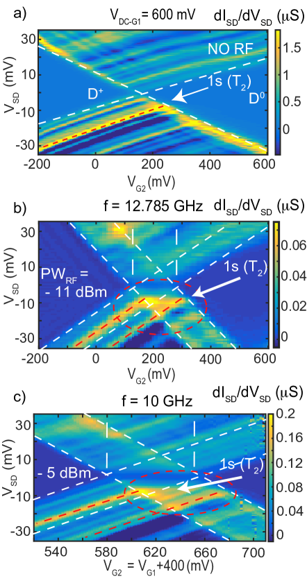
In Fig. 3 b) we now present the same spectrum but with an rf excitation of = 12.785 GHz applied to G1. We observe the same doubling of current signature as observed in Fig. 2c), but now for the excited state spectrum, e.g. 1s(). This first excited state is located at 10 meV 2 meV, consistent with the previously measured bulk value for the first excited state of a single P donor in bulk silicon Fue242 ; Fue2011 ; Ram1297 as shown in Fig. 1c). Likewise in Fig. 3 c) we observe the same effect but now using an rf excitation at = 10 GHz applied to G1 and with both gates addressed in dc, as in Fig. 2. These results are similar to those discussed in Fig. 2d), however this time the capacitive coupling is demonstrated for the 1s() level of the excited state spectrum and shows robustness to the electric field across the donor.
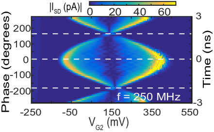
Quantum information and quantum metrology applications require precise and independent rf control of different gates, Loss120 ; Hill15 ; Fuj207 as many quantum logic gate operations include fast manipulation of electron states. These operations require the absolute synchronisation in phase (time) between the rf signal individually applied to different gates and of their relative coupling to quantum states. To ascertain if this is possible in our device, in Fig. 4 we present results obtained from applying sinusoidal rf excitations of 250 MHz to the bias-tees of both G1 and G2. Here, the provided rf excitations are of equal amplitude but there is a varying difference in the absolute phase between the two signals. Hence, Fig. 4 ultimately allows to quantify the level of synchronisation in time between the capacitive coupling between G1 and the GS and the one between G2 and the GS. The result of these measurements confirms that, within the limit of precision of the source ( 10 ps, see methods section), a very similar capacitive coupling between each gate and the donor state Fue2011 is in place and is preserved in the rf regime. These results show that, by precision STM patterning, it is possible to have control of the device symmetry and, as a result, to observe accurate nanosecond synchronisation between different gates up to 0.25 GHz frequencies. The results presented so far are of relevance for the field of quantum computations as they demonstrate the control of energy states at 10 GHz, i.e. the high frequencies required for several quantum computer proposals which, require synchronous sub-ns pulses to be applied to quantum states Loss120 ; Hill15 . Precision transistors can also be used for single-electron transfer applications, such as the ones necessary for quantum metrology, Tet063036 ; Fuj207 where independent and precise control in time of more than one gate is needed.
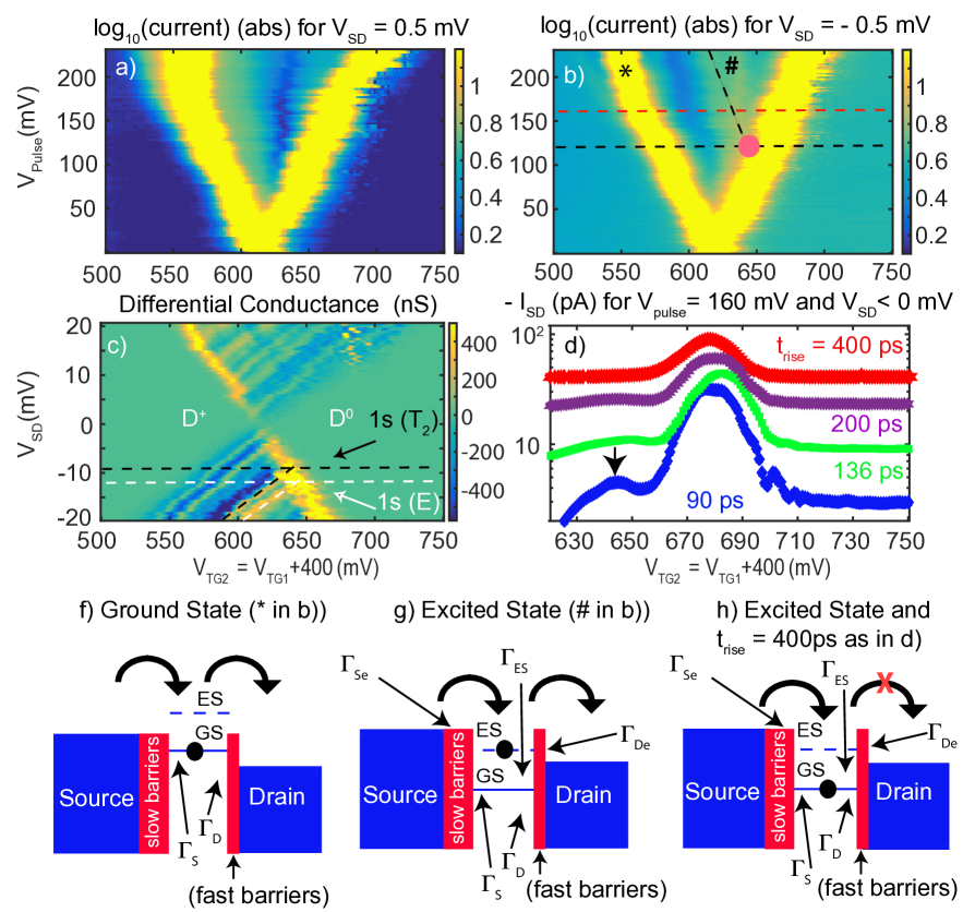
In the next section we shall show how, using excited state spectroscopy at = 50 MHz, Fuj081304 ; Volk1753 we can distinguish the electron excited states spectrum of the donor from the 1D confinement-related DOS of the quasi one dimensional leads. Fue242 ; Fue2011 ; Ryu374 ; Mot161304 As in the previous experiments, when we apply a square wave signal to one of gates addressing the state, we observe a characteristic V-shape of the current as a function of increasing pulse voltage (see Fig. 5 where represents the voltage amplitude provided to the bias-tee). The V-shape of the current represents the doubling of the ground state peak when square pulses are applied to G1 and is observed both for positive (Fig. 5a) and for negative (Fig. 5b) source bias voltages. This process is schematically described in Fig. 5f) for negative biases. In Fig. 5 a) and b) the left branch shows the current where the ground state is pulsed from far above the bias window, while the right branch represents the dc ground state signature, which is shifted by the introduction of the pulse. There is an additional feature, labelled ””, observed when a negative bias is applied to the source, as in Fig. 5 b), which we attribute to the excited state of the donor electron as explained in the next section. It is worthwhile to remember that the DOS in the one dimensional leads cannot be associated with this additional feature because the DOS signature is not -dependent but only S/D bias-dependent. Fue242 ; Fue2011 ; Mot161304 Hence, in these experiments we can address both the excited and ground state spectrum at low bias such that pulse spectroscopy allows to distinguish transport via the excited state and the DOS in the leads in a way not possible via dc spectroscopy. Fue242 ; Fue2011 The Coulomb diamonds and the doubling observed in Fig. 5 a) and b) allow a direct conversion between gate voltage and energy. From the position of the red dot in Fig. 5b) at = 120 mV 10 mV and using 0.075 for the final correction factor of the applied power (see methods section), we can determine an excited state energy of 9 meV 1 meV.
This pulsed-estimated value for the excited state energy 1s() lies close to the one extracted from the dc data in Fig. 5c) 10 meV 2 meV (black arrow and black dashed lines), see also red ellipses and red dashed lines in Fig. 3b) and Fig. 3c). The position of the other visible peak for the excited state (1s(E), white arrow and white dashed line around 13.5 meV), is also very close to the expected bulk values, i.e. 11.7 meV and from previous estimations made of this device, in the dc mode. Fue242 ; Fue2011
It is important to understand why the overall dc excited state spectrum is more visible for negative bias (e.g. see Fig. 5 c)) which indicates that the transparencies of the source/drain to excited state barriers (/) are asymmetric, with the latter being more transparent. Fue2011 ; Lan136602 The asymmetry in the tunnel barriers (i.e. / 1) can be better understood by looking at Fig. 5g) where the negative bias regime is schematically illustrated. This figure shows that if the electrons moving from source to drain via the excited state encounter first a slow barrier, , and then a fast one, , then the dc excited state signature will be more visible compared to the opposite case of positive bias where an electron will first encounter a fast barrier and then a slow one. In the later case electrons are most likely to relax to the ground state before tunnelling through the slow barrier and the excited state signature will be less visible. Furthermore, as the same asymmetry applies for pulsing experiments and, at negative bias and for sufficiently slow relaxation from the 1s () excited state to the ground state, , if compared with , we see the excited state line once the pulse amplitude exceeds the ES energy (black dashed line, the pale red dot and the symbol in Fig. 5b)). This because the asymmetry will allows a better visibility of the excited state 1s () but this time at low bias and without the presence of the DOS signature complicating the picture. It can be easily seen Fue2011 that the same asymmetry observed in the tunnel barriers / is also true for / with and being the source to ground state and the drain to ground state barriers, respectively, where the following two inequalities can also be obtained: Fuj081304 ; Volk1753 ; Tah075302
| (1) |
| (2) |
where these two inequalities are due to the typical larger spatial extent of the excited state wave functions compared to the ground state ones.
The values of the two barriers and have been already quantified via a simple modelling111The estimation of these rates comes from the assumption that, in this device, the transport at low temperatures ( 100 mK) is in the life time broadening regime which allow to extract a first set of indicative values for the values of 150 MHz and 164.5 GHz, see also Ref Fue2011 . to be 150 MHz and 164.5 GHz confirming the expected asymmetry of the barriers (/ ), not unusual for these systems. Lan136602 Since Eq. 2 is true, it follows that . As a consequence we can obtain bounds for from the following points:
-
•
The rise time from 10 to 90 of the maximum amplitude Fuj081304 ; Volk1753 of the used pulsed signal is 90 ps (11 GHz), hence the pulse brings the excited state in resonance within this 11 GHz range of frequencies. This gives us the information that is 11 GHz in agreement with what already discussed.
-
•
The amplitude of the excited state signal in Fig. 5b) is 4 pA, hence it is possible to estimate that 50 of the electrons are loaded via the excited state during each individual pulse. Also, the edge of the square pulse Fuj081304 ; Volk1753 can never be sharp as in an ideal case, hence this indicates that cannot be much faster than , in agreement with Equ. 1.
-
•
If a positive bias is applied to the device, as in Fig. 5a), the electrons first encounter the fast barrier and then the slow one, . As no extra signal can be observed for this regime, this indicates that the electrons are always relaxing to the ground state before being able to tunnel to the source, leading to the conclusion that , in agreement with recent theoretical estimations. Tah075302
The set of observations just discussed together with and Eq. 1 and Eq. 2 allow us to determine approximative bounds for as in the following inequalities: , hence 164.5 GHz 150 MHz. To test this hypothesis further, in Fig. 5d) traces are taken for a fixed = 160 mV (as in the red dashed line in Fig. 5b)) across the excited state signal. Here we can see by adding different low pass filters to the pulse line (at room temperature and one at the time) we can change the pulse rise time and observe if the extra signal related to the excited state can be attenuated. In fact, by increasing the rise time of the pulse to 400 ps (i.e. by using a 2.5 GHz low pass filter), the extra signal can be completely suppressed. As shown schematically in Fig. 5g) and in ref., Fuj081304 ; Volk1753 the fast rise time of the pulse is a fundamental requirement for the observation of the resonant tunnelling via the excited state. If the rise of the pulse edge is too slow compared to and , then the electrons cannot resonantly tunnel via the excited state but instead have always an higher chance to first tunnel to the ground state cancelling the possibility of observing the extra current signature.
Here we argue that the use of the filters and the reduction of the rise time to 400 ps ultimately favours tunnelling via the ground state rather than via the excited state. This allows us to give a better estimation of the value for 2.5 GHz, since only when the rise time and have similar values can the extra signal related to the resonant tunnelling via the excited state be suppressed. Note that this value of is higher than the value of extracted from dc transport,11footnotemark: 1 but still realistic. This correction on the estimation of , leads also to a slightly improved estimation of 162 GHz,11footnotemark: 1 while still confirming the asymmetry between the two barrier rates.
The use of filters described above and schematically drawn in Fig. 5h) can provide a rough estimate for , since it is not easy to determine the final influence that the filter has to the shape of the pulse, Fuj081304 ; Volk1753 however it gives a better indication for the bounds of . In fact, this discussion suggests that a better defined range for the value of is: 162 GHz 2.5 GHz, which is compatible with theoretical predictions and with experimental observations. Tah075302 ; Zhu093104 ; HubS211 We have shown how to extract limits for the value of the relaxation rate of the first excited state of an isolated P donor. As traditionally these quantities are difficult to measure Fuj081304 ; Volk1753 ; Zhu093104 ; HubS211 or estimate theoretically Tah075302 ; Riw235401 this is a relevant result for the fields of Si quantum information and Si quantum metrology. In these planar doped devices the barriers and are tuneable only during fabrication allowing us to control the tunnel rates by an order of magnitude with precision lithography using current techniques, with future experiments aimed at improving this further. Cam2013 This non tunability of the barriers during experiments represents an ultimate limit to the pulsing frequency that can be used. Hence, the higher pulse frequency, of the same order of magnitude as the relaxation rates 10 GHz, necessary to obtain a quantitative value Fuj081304 ; Volk1753 of as in Refs. Zhu093104 ; HubS211 ; Tah075302 is not accessible. However, the regime explored in these experiments demonstrates the potential of the fast pulsing technique with all epitaxial monolayer doped gates. The discussion contained in this last section also explains why no excited state substructure can be observed in this Fig. 2, as the use of a sinusoidal excitation doesn’t provide the appropriate conditions (as in Fig. 5g)) for the electrons to resonantly tunnel via excited states when the S/D bias is small.
CONCLUSIONS
In conclusion, in this work we demonstrated fast rf control of the excited state spectrum of a atom in a single atom transistor using all epitaxial monolayer doped gates. This control was performed at GHz speed and with nanosecond synchronisation needed to execute quantum gate operations in several silicon based quantum computer proposals. Pulsed spectroscopy measurements with selective transport via excited states allowed us to differentiate between the excited states of the single atom and the density of states in the one dimensional leads in a manner not possible via dc spectroscopy. From these measurements we demonstrated a possible range of values for the relaxation times from the first excited state to the ground state. Such excited state relaxation rate information will help in the assessment on how realistic is the use of the silicon quantum valley-orbital degree of freedom for quantum logic and quantum metrology applications. Riw235401 ; Tet046803 ; Cul126804 This work shows that with precision single atom fabrication technologies with epitaxial monolayer doped gates we can apply voltages up to GHz frequencies to control the spin states of the qubits. With the recent demonstration of the suppression of charge noise in these systems Sha233304 ; Sha236602 ; Sha3 this bodes well for precision donor based qubits in silicon.
ACKNOWLEDGMENTS
G. C. Tettamanzi acknowledges financial support from the ARC-Discovery Early Career Research Award (ARC-DECRA) scheme, project title : Single Atom Based Quantum Metrology and ID: DE120100702 for the development of the setup used in these experiments. M.Y.S. acknowledge a Laureate Fellowship (FL130100171).
METHODS AND EXPERIMENTAL
Fabrication of the Single Atom Transistor Device. The device is fabricated on a low-doped (1-10 cm) silicon wafer prepared with a Si(100) 2x1 surface reconstruction using a flash anneal to 1150 ∘C, before it is passivated by atomic hydrogen. Controlled voltage and current pulses on the STM tip locally desorb this hydrogen layer to define the device features with atomic precision, leaving behind chemically active Si unpaired bonds. PH3 gas introduced into the chamber binds to the surface in the regions where the hydrogen was desorbed. An anneal to 350 ∘C causes the P atoms to incorporate into the top layer of the Si crystal. The P doped features are then encapsulated by low temperature ( 250 oC) solid source Si molecular beam epitaxy. The all epitaxial doped leads are electrically contacted by first using reactive ion etching to etch holes in the encapsulation down to the doped layer, then the holes are filled by evaporation of Al to make ohmic contact to the P doped layer. The P doped leads in this device are 1000 nm long and widen between 5 nm in the central part of the device to 800 nm in the contact region, with in an estimated 36 of two terminal resistance along the length of the leads. Fue2011
Low Temperature and rf Measurements. The device is mounted on a cold finger of 4He pot of an Oxford Variable Temperature Insert (VTI) operated at 1.2 K. A low noise battery operated measurement setup was used to measure the source/drain current and to apply the dc voltages. To apply the sinusoidal rf input to the gates via the bias-tees an Agilent E8257C source (operating up to 40 GHz) and a two channels Agilent 81180A source were used. The inter-channel time skew control of the Agilent 81180A source goes from -3 ns to +3 ns with 10-ps precision and determines the best possible control in time/phase between the two different rf signals (10-ps which is equivalent to 0.9 degrees for the used = 250 MHz of our experiments). rf signals can be transferred to the bias-tees via high performance coax rf lines.
These lines have silver-plated copper-nickel inner conductor and copper-nickel outer conductor (i.e. attenuation ranging between the sub dBm/m to the few dBm/m at 20 GHz). SK coaxial rf connectors are used in all these rf lines and 6 dBm attenuators are placed as close as possible to the bonding pads ( 1 cm). The bias-tees are built with typical resistance and capacitance values of R = 1 M and C = 1 nF, respectively. The used values for R and for C leads to characteristic RC times of around the few ms and high pass filter cutting frequencies of around a 0.1 KHz. These bias-tees have also been tested independently with a Keysight N9918A FieldFox handheld microwave analyser and have shown to operate with no resonances and with the expected linear increases of the losses up to the 26.5 GHz (i.e. the limit of our analyser).
Furthermore, a correction factor 0.75 estimated via the of the V-shape in Fig. 5a) and in Fig. 5b) is used to take into account the attenuation of the signal at the bias-tee level (for = 50 MHz) while the gate lever arm has been already estimated to 0.1 Fue2011 making the final correction factor of the applied power equal to 0.075. Indeed, experiments as shown in Fig. 2 have been possible up to 20 GHz, knowing that neither the rf source or attenuation in the rf lines are a limitation to these experiments for up to 40 GHz and the bias-tees attenuation is not a limitation to these experiments for up to 26.5 GHz. The limitation on the maximum frequency of operation of our device is most likely due to imperfect 50 matching at the interface between the Al/Si bonding wire and the bonding pad of the device (used to connect the device to the external setup). The pulsing experiments have been performed with an HP 8131 and with an Agilent 81180A AWG in combination with a fast switching optical isolator from Delft university (http://qtwork.tudelft.nl/ schouten/ivvi/doc-mod/docs5d.htm). Overall, the 10 to 90 rising time was estimated with a fast oscilloscope to be 90 ps for the pulses used in Fig. 5, hence we believe that the AWG is not a limiting factor to the excited state spectroscopy experiments.
ADDENDUM
In our paper we provided an upper bound for the relaxation from the 1s () excited state to the ground state, . This was determined from our estimation that the drain to ground state fast tunnel barrier, was equal to 162 GHz. We have now realised that in Figure 5g) of the paper, where the transport mechanisms that allowed the observation of the excited state signature are schematically explained, we neglected to consider the process where an electron tunnels from drain to the ground state, see green arrow in Figure 6 below. This neglected process can lead to blockading of the loading of the excited state, which no longer contributes to a net current through the Single Atom Transistor. The fact that we nevertheless observe the excited state resonance in the experiment suggests that the rate for this loading (i.e. ) is not greater than the source to excited state () as previously estimated and is much smaller than 162 GHz. It does however indicate that these two rates are of the same order of magnitude, and the competition between the two processes contributes to the observed current (4 pA). This interpretation is a minor adjustment to that given in the paper, only requiring and being of the same order of magnitude while being much smaller than . In this new interpretation of the data the estimation of the source to ground state slow tunnel barrier, , being much smaller of is confirmed. The same applies for the lower bound for obtained in the paper and discussed in the abstract. However, it is no longer possible to estimate an higher bound for the value of the which was previously stated as 162 GHz.

References
- (1)
- (2)