Counting Near Infrared Photons with Microwave Kinetic Inductance Detectors
Abstract
We demonstrate photon counting at 1550 nm wavelength using microwave kinetic inductance detectors (MKIDs) made from TiN/Ti/TiN trilayer films with superconducting transition temperature 1.4 K. The detectors have a lumped-element design with a large interdigitated capacitor covered by aluminum and inductive photon absorbers whose volume ranges from 0.4 m3 to 20 m3. The energy resolution improves as the absorber volume is reduced. We achieved an energy resolution of 0.22 eV and resolved up to 7 photons per optical pulse, both greatly improved from previously reported results at 1550 nm wavelength using MKIDs. Further improvements are possible by optimizing the optical coupling to maximize photon absorption into the inductive absorber.
Photon-number-resolving (PNR) detectors at near infrared wavelengths have important applications in a number of frontier fields, such as quantum secure communications Hiskett , linear optical quantum computing Knill and optical quantum metrology Zwinkels . Compared to more conventional detectors at this wavelength, such as silicon-based detectors Finger , superconducting detectors have lower dark-count rate, higher sensitivity, and broadband response. They show great promise in serving as the basic building blocks for efficient PNR devices. For example, by spatial or temporal multiplexing of superconducting nanowire single-photon detectors (SNSPDs) Tsman ; Divochiy ; Dauler ; Mattioli , photons can be counted at high speed. But the single-element nanowire has no intrinsic PNR and energy-resolving capabilities. Alternatively, single-element transition edge sensors (TESs) Irwin have demonstrated high quantum efficiency and multi-photon discrimination at telecommunication wavelengths Miller ; Lita ; Calkin . Recently, counting up to 29 photons and intrinsic energy resolution eV at nm wavelength have been achieved in Ti/Au TESs Lolli ; Lolli2 ; Lolli3 .
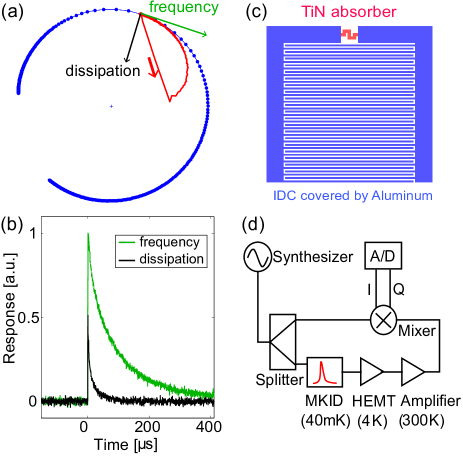
Another type of superconducting detector possessing intrinsic photon-number-resolving and energy-resolving power is the microwave kinetic inductance detector (MKID) Day . MKIDs are cooper pair breaking detectors based on high-quality factor (high-) superconducting resonators zmuidzinas ; yiwen . The absorption of a photon with energy higher than twice the gap energy () can break Cooper pairs into quasiparticles, changing the surface impedance of the resonator and resulting in a lower resonance frequency and higher internal dissipation (or lower quality factor ). When applying a short optical pulse to the detector and probing the resonator with a microwave tone near the resonance frequency, one can obtain a pulse response in the complex forward transmission , as shown in Fig. 1(a). This photon response can be measured using a homodyne detection scheme (Fig. 1(d)) and the signal can be decomposed into frequency and dissipation responses (Fig. 1(a),(b)) for pulse analysis.
Compared to TESs, MKIDs are easy to fabricate and multiplex into large arrays. A large array of MKIDs can be measured using a pair of coaxial cables, which greatly reduces the complexity of the instrument design. Previously, MKIDs with PNR capability have mostly been considered for astronomy applications at the visible wavelength Bumble . Single-photon counting at telecommunication wavelengths (near infrared) with titanium-nitride (TiN) MKIDs was first demonstrated in Ref. Jiansong , where a full-width-at-half-maximum (FWHM) energy resolution 0.4 eV was achieved and up to 2-photon events were resolved. In this letter, we present an optimized MKID design based on TiN/Ti/TiN trilayer films and improved photon counting performance at 1550 nm wavelength: energy resolution 0.22 eV is obtained and up to 7-photon events can be resolved.
Our detectors are made from a 20 nm thick TiN/Ti/TiN trilayer film Vissers ( K) deposited on a high-resistivity Si substrate. Such TiN trilayer films were initially developed for feedhorn-coupled MKIDs which have recently demonstrated photon-noise limited sensitivity at submillimeter wavelengths hannes . As shown in Fig. 1(c), our detectors comprise a large IDC shunted by a meandered inductive strip. The latter serves as a sensitive photon absorber. The IDC area is 0.7 mm 0.7 mm, with m finger/gap width. This large area IDC is used to suppress the two-level system (TLS) noise in the substrate gao2008 . The IDC is covered with a 100 nm-thick layer of aluminum (Al). Because of the low current density in the IDC and the much lower kinetic inductance of Al than TiN, the response from a photon hitting the IDC area is negligible. We designed resonators on a 10 mm by 5 mm chip, with inductor strip width ranging from 1 m to 20 m, length from 10 m to 100 m and volume from 0.4 m3 to 20 m3, to systematically study the dependence of the detector performance on the absorber geometry. All the resonance frequencies are designed to be around GHz and all the resonators are coupled to a common microstrip feedline with coupling quality factor .
The detectors are cooled in a dilution refrigerator to a base temperature of 40 mK. At this temperature, the internal quality factors of the resonators are measured to be around . A 1550 nm laser diode driven by a function generator at room temperature is used to generate optical pulses with a width of 200 ns at a repetition frequency of 120 Hz. The incident photons are then attenuated and guided into the device box mounted at the mixing chamber stage through a bare optical fiber. In this demonstration experiment, we did not optimize the optical coupling to the absorber and the light exiting the fiber flood illuminates the entire chip instead of being focused only onto the absorber area. As a result, the optical efficiency is rather low, which we plan to improve in future experiments. As shown in Fig. 1(d), the standard homodyne scheme is used to read out the resonators. We probe the resonators at a microwave frequency that maximizes the frequency response and the microwave power is chosen to be 2 dB below bifurcation power to avoid the strong non-linear effects zmuidzinas in the resonator. For each optical pulse, the corresponding response of the detector is digitized at a sampling rate of 2.5 Ms/s. The raw data are converted to the frequency and dissipation responses. Only the frequency response data are further analyzed, because the dissipation response is smaller compared to the frequency response and the dissipation pulse decay time is much faster (see Fig1. (b))due to the anomalous electrodynamic effect found previously in TiN films PropTiN ; Jiansong ; hannes . Note that we have used a rigorous non-linear fitting procedure to directly convert the pulse trajectory in the IQ plane to the fractional frequency shift, because the response in fractional frequency shift unit is always linearly proportional to the change in the quasiparticle density, even when the pulse response is large (approaching the resonator line-width) and the phase shift becomes nonlinear. We analyze the pulse data by using standard Weiner optimal filter procedures and the filtered pulse height data are used to generate photon-counting statistics.
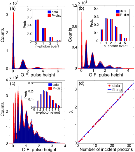
Fig. 2(a) shows a histogram of the optimally filtered pulse height data for 2 pulse events measured from the resonator with absorber width of 2 m and volume of 1.92 m3. The first 3 peaks, which correspond to the events of 0, 1, and 2 photons being absorbed in the detector, are clearly observed. We fit the histogram to a model of a superposition of 4 Gaussian peaks with independent heights and widths, as shown by the red profile in Fig. 2(a). The FWHM energy resolution of the -photon peak is related to the standard deviation of the -th Gaussian peak by:
| (1) |
where eV is the energy of a single 1550 nm photon and is the pulse height of the -photon peak. The obtained FWHM energy resolutions for the 1-photon and 2-photon peaks are 0.34 eV and 0.42 eV respectively. Here we claim a peak is resolved if . According to this criterion, this detector has the sensitivity to resolve the first 3 peaks (0-, 1- and 2-photon). According to the stochastic nature of the photon detection process, the -photon events should obey Poisson statistics. Indeed, as shown in the inset of Fig. 2(a), the counts in the -photon peak (proportional to the area of each Gaussian) normalized by the total counts match a Poisson distribution with 0.61. is the mean photon number absorbed by the detector, suggesting that our detector detects an average of 0.61 photons per pulse event.
Fig. 2(b) shows the photon counting histogram at a higher input optical power, corresponding to a mean photon number 1.95. The first 6 (0- to 5-photon) peaks are resolved with the energy resolutions of 0.36 eV and 0.45 eV for the 1-, and 2-photon peak respectively, which both slightly increase from Fig. 2(a). Fig. 2(c) shows the histogram at an even higher optical power with a mean photon number of 3.78, where the first 8 (0- to 7-photon) peaks are resolved.
In the 3 histograms shown in Fig. 2, we see that the 1- and 2-photon peaks are clearly broadened as compared to the 0-photon peak, indicating that additional noise arises when photons are absorbed and the energy resolution for the -photon peak () is not dominated by the background noise of the detector in the dark environment. We speculate the broadening might be related to several factors, including position-dependent response of the absorber, parasitic response from the photons hitting the non-absorber area (e.g., IDC, substrate, feedline), some unknown sources of photon-induced noise. We have simulated the current distribution using Sonnet (an electromagnetic simulation software) and the results show that the current is very uniform throughout the inductor strip to be within 0.4. This is expected because the dimensions of the inductors (m) are much smaller than the microwave wavelength ( cm around 6 GHz). Since the resonator frequency response is proportional to the local kinetic inductance change weighted by the square of the current distribution gaothesis , broadening of the photon peak due should not be dominated by the non-uniform current distribution in the inductive absorber.
In Fig. 2(d), we plot the detected mean photon number as a function of the estimated total number of photons incident onto the absorber area, which is perfectly linear as expected. The incident photon number is estimated from the total optical power measured by a power meter and the solid angle covered by the absorber area at the distance from the absorber to the fiber tip. Due to the low photon absorption efficiency, our detector can absorb and detect only 1 photon for approximately incoming photons hitting the absorber.
In this work, we have 13 resonators with different absorber volumes, which allows us to compare the photon counting statistics. The main results are summarized in Fig. 3. Fig. 3(a) shows the 1-photon responsivity (fractional frequency shift induced by absorbing 1 photon) as a function of the absorber volume . The measured responsivity is fitted well by a linear relation with . This is expected because , where is the quasiparticle density.
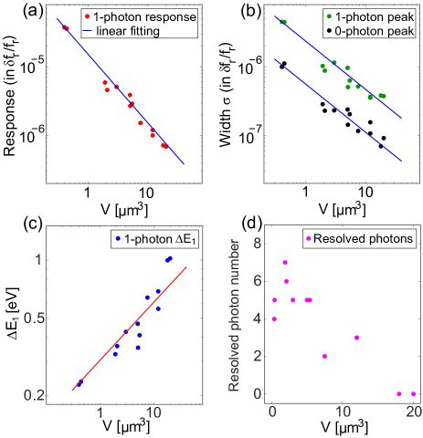
Fig. 3(b) shows the widths (i.e., the standard deviations and converted to which is a measure of the frequency noise) of the 0-photon peak (black dots) and 1-photon peak (green dots) as a function of . Both widths roughly fit onto a power-law of and the 1-photon peak is about 4.5 times wider than the 0-photon peak. Combining the responsivity data from Fig. 3(a) and the noise data from Fig. 3(b), we derive the 1-photon energy resolution from Eqn. (1) as a function of , which is plotted in Fig. 3(c). We see that increases with and scales as . Our results suggest that the energy resolution improves as the absorber volume is reduced. The best we obtained is 0.22 eV, corresponding to an energy-resolving power of at 1550 nm, which is achieved in the resonator with the smallest absorber volume of 0.4 m3 and also the narrowest inductor width of 1 m. In Fig. 3(d), we plot the maximum number of photons that can be resolved by each detector as a function of its absorber volume . We see that drops at both smallest and largest . drops at large because the energy resolution degrades as is increased (Fig. 3(c)). also drops at small because the large responsivity and high photon number lead to “saturation” of the detector, where the frequency shift of the pulse exceeds the resonator bandwidth and the signal-to-noise ratio is degraded. To increase the bandwidth for operation, we can design resonator with lower and/or higher resonance frequency .
The best theoretical energy-resolving power that can be achieved by a MKID as a pair-breaking detector is given by , where is the conversion efficiency from photons to quasiparticles STJ , is the energy of the incident photons, is the superconducting gap energy of the absorber material, and is the Fano factor Fano . This predicts a theoretical at 1550 nm (a typical value of is assumed), which is an order of magnitude higher than the achieved by our best detector. Coincidentally, the optical lumped-element MKIDs Marsden ; Marsden2 made from 20-60 nm substoichiometric TiN films have a typical energy-resolving power at 254 nm, which is also an order of magnitude below their Fano limit . While this suggests that TiN-based photon counting detectors have large room to improve, it is important to understand why they “underperform” their theoretical prediction. In fact, is the ideal conversion efficiency when photons are absorbed in a bulk superconductor. Our film is only nm thick and the high energy phonons may quickly escape the film into the substrate before breaking more quasiparticles, leading to a efficiency smaller than and a smaller response. This phonon loss process may also fluctuate and cause additional noise, as observed in the thin film superconducting tunnel junction photon detectors STJ . In future experiments, we plan to futher explore this phonon loss effect, as well as the energy resolution scaling, by testing different thickness of TiN films and by making the absorber on a suspended membrane.
Many aspects in our design and experimental setup can be improved. If the responsivity and noise trends still hold below 0.4 m3, we expect that better energy resolution can be achieved by using an absorber volume even smaller than 0.1 m3. Instead of using 1.4 K trilayer, a lower TiN film with a lower gap energy may further boost the responsivity. Suspending the absorber on a thin silicon membrane may increase the quasiparticle recombination time and the conversion efficiency, as suggested by the “phonon recycling” scheme Fyhrie ; Ulbricht . According to the optical measurement on thin TiN films by VolkonenValkonen , we estimate that the reflectance and transmittance for our 20 nm TiN film are about 60 and 10 respectively, indicating approximately only 30 photons are absorbed. The photon absorption efficiency can be greatly enhanced by adding anti-reflection coating and embedding the absorber in an optical structure Lita2 . To efficiently collect every photon, the input light should be precisely confined onto the absorber active area, which can be realized using advanced alignment and coupling techniques, such as direct fiber coupling to the detector Miller2 or through a fusion-spliced microlens Dauler2 .
In conclusion, we have demonstrated photon counting at 1550 nm using TiN/Ti/TiN trilayer MKIDs. Energy resolution as low as 0.22 eV is obtained and up to 7-photon events can be resolved. By studying devices with a variety of geometries, we have systematically investigated the dependence of photon counting performance on the absorber volume. The energy resolution improves as the absorber volume is reduced. Further improvements in these detectors are possible by improving the detector design and optimizing the optical coupling to maximize the photon absorption into the absorber. With the energy resolution of our MKID photon counting detectors approaching the performance of TESs (currently a factor of two better), the multiplexing advantage of MKIDs may stand out in applications where a large array of detectors with high photon-resolving power is needed.
The MKID devices were fabricated in the NIST-Boulder microfabrication facility. This work was supported in part by the National Natural Science Foundation of China (Grant Nos. 61301031, U1330201). L. F. Wei thanks Profs. C. D. Xie and K. C. Peng for their encouragements and useful discussions.
References
- (1) P. Hiskett, D. Rosenberg, C. Peterson, R. Hughes, S. Nam, A. Lita, A. Miller, and J. Nordholt, New J. Phys. 8, 193 (2006).
- (2) E. Knill, R. Laflamme, and G. J. Milburn, Nature 409, 46 (2012).
- (3) J. Zwinkels, E. Ikonen, N. Fox, G. Ulm, and M. Rastello, Metrologia 47, R15 (2010).
- (4) G. Finger, I. Baker, D. Alvarez, D. Ives, L. Mehrgan, M. Meyer, J. Stegmeier and H. J. Weller, Proc. of SPIE 9148, 914817 (2014).
- (5) G. Gol’tsman, O. Okunev, G. Chulkova, A. Lipatov, A. Semenov, K. Smirnov, B. Voronov, A. Dzardanov, C. Williams and R. Sobolewski, Appl. Phys. Lett. 79, 705 (2001).
- (6) A. Divochiy, F. Marsili, D. Bitauld, A. Gaggero, R. Leoni, F. Mattioli, A. Korneev, V. Seleznev, N. Kaurova, O. Minaeva, G. Gol’tsman, K. Lagoudakis, M. Benkhaoul, F. Levy, and A. Fiore, Nature Photonics 2, 302 (2008).
- (7) E. Dauler, A. Kerman, B. Robinson, J. Yang, B. Voronov, G. Goltsman, S. Hamilton, and K. Berggren, Journal of Modern Optics 56, 364 (2009).
- (8) F. Mattioli, Z. Zhou, A. Gaggero, R. Gaudio, R. Leoni, and A. Fiore, Optics Express 24, 9067 (2016).
- (9) K. D. Irwin, Appl. Phys. Lett. 66, 1998 (1995).
- (10) A. J. Miller, S. W. Nam, J. M. Martinis, and A. V. Sergienko, Appl. Phys. Lett. 83, 791 (2003).
- (11) A. Lita, A. Miller and S. Nam, Optics Express 16, 3032 (2008).
- (12) B. Calkins, P. Mennea, A. Lita, B. Metcalf, W. Kolthammer, A. Linares, J. Spring, P. Humphreys, R. Mirin, J. Gates, et al., Optics Express 21, 22657 (2013).
- (13) L. Lolli, E. Taralli, and M. Rajteri, J Low Temp Phys 167, 803 (2012).
- (14) G. Brida, L. Ciavarella, I. Degiovanni, M. Genovese, L. Lolli, M. Mingolla, F. Piacentini, M. Rajteri, E. Taralli, and M. Paris, New. J. Phys. 14, 085001 (2012).
- (15) L. Lolli, E. Taralli, C. Portesi, E. Monticone, and M. Rajteri, Appl. Phys. Lett. 103, 041107 (2013).
- (16) P. K. Day, H. G. LeDuc, B. A. Mazin, A. Vayonakis, and J. Zmuidzinas, Nature 425, 817 (2003).
- (17) J. Zmuidzinas, Annual Review of Condensed Matter Physics 3, 169 (2012).
- (18) Y. Wang, P. Zhou, L. Wei, H. Li, B. Zhang, M. Zhang, Q. Wei, Y. Fang, and Chunhai Cao, J. Appl. Phys. 114, 153109 (2013).
- (19) B. A. Mazin, B. Bumble, S. R. Meeker, K. O Brien, S. McHugh, and E. Langman, Opt. Express 20, 1503 (2012).
- (20) J. Gao, M. Vissers, M. Sandberg, F. Silva, S. Nam, D. Pappas, D. Wisbey, E. Langman, S. Meeker, B. Mazin H. Leduc, J. Zmuidzinas, and K. Irwin, Appl. Phys. Lett. 101, 142602 (2012).
- (21) M.R. Vissers, J. Gao, M. Sandberg, S. M. Duff, D. S. Wisbey, K.D. Irwin, and D. P. Pappas. Appl. Phys. Lett. 102, 232603 (2013).
- (22) J. Hubmayr, J. Beall, D. Becker, H.-M. Cho, M. Devlin, B. Dober, C. Groppi, G. C. Hilton, K. D. Irwin, D. Li, P. Mauskopf, D. P. Pappas, J. Van Lanen, M. Vissers, Y. Wang, L. F. Wei, and J. Gao, Appl. Phys. Lett. 106, 073505 (2015).
- (23) J. Gao, M. Daal, J. Martinis, A. Vayonakis, J. Zmuidzinas, B. Sadoulet, B. Mazin, P. Day, and H. Leduc, Appl. Phys. Lett. 92, 212504 (2008).
- (24) J. Gao, M. R. Vissers, M. Sandberg, D. Li, H. M. Cho, C. Bockstiegel, B. A. Mazin, H. G. Leduc, S. Chaudhuri, D. P. Pappas,and K. D. Irwin, J Low Temp Phys, 176, 136 (2014).
- (25) J. Gao, Ph.D. thesis, Caltech, 2008.
- (26) D. D. E. Martin, P. Verhoeve, A. Peacock, A. G. Kozorezov, J. K. Wigmore, H. Rogalla, and R. Venn, Appl. Phys. Lett. 88, 123510 (2006).
- (27) U. Fano, Phys. Rev. 72, 26(1947).
- (28) D. Marsden, B. A. Mazin, B. Bumble, Seth Meeker, K. O’Brien, S. McHugh, M. Strader, and E. Langman, Proc. SPIE 8453, 84530B (2012).
- (29) B. A. Mazin, S. R. Meeker, M. J. Strader, P. Szypryt, D. Marsden, J. C. van Eyken, G. E. Duggan, A. B. Walter, G. Ulbricht, M. Johnson, B. Bumble, K. O’Brien, and C. Stoughton, Publications of the Astronomical Society of the Pacific, 125, 1348 (2013).
- (30) A. Fyhrie, C. McKenney, J. Glenn, H. G. LeDuc, J. Gao, P. Day, and Jonas Zmuidzinas, Proc. SPIE 9914, 99142B (2012).
- (31) G. Ulbricht, B. A. Mazin, P. Szypryt, A. B. Walter, C. Bockstiegel, and B. Bumble, Appl. Phys. Lett. 106, 251103 (2015).
- (32) E. Valkonen, C. Ribbing, and J. Sundgren, Applied Optics 25, 3624 (1986).
- (33) A. Lita, B. Calkins, L. Pellouchoud, A. Miller, and S. Nam, Proc. of SPIE 7681, 76810D-1 (2010).
- (34) A. Miller, A. Lita, B. Calkins, I. Vayshenker, S. Gruber, and S. Nam, Optics Express 19, 9102 (2011).
- (35) E. A. Dauler, M. E. Grein, A. J. Kerman, F. Marsili, S. Miki, S. W. Nam, M. D. Shaw, H. Terai, V. B. Verma, and T. Yamashita, Opt. Eng. 53, 081907 (2014).