,
Effect of uniaxial strain on the optical Drude scattering in graphene
Abstract
Graphene is a mechanically robust 2D material promising for flexible optoelectronic applications. However, its electromagnetic properties under strain are experimentally poorly understood. Here we present the far-infrared transmission spectra of large-area chemical-vapor deposited monolayer graphene on a polyethylene terephthalate substrate subjected to uniaxial strain. The effective strain value is calibrated using the Raman spectroscopy and corrected for a relaxation of wrinkles and folds seen directly by atomic-force microscopy. We find that while the Drude weight and the Fermi level remain constant, the scattering rate increases by more than 10% per 1% of applied strain, showing a high level of reproducibility during strain cycling. As a result, the electronic mobility and optical absorption of graphene at terahertz and lower frequencies appear to also be sensitive to strain, which opens pathways to control these key parameters mechanically. We suggest that such a functionality can be potentially used in flexible optoelectronic and microelectromechanical systems based on graphene. By combining our findings with existing theoretical models, we discuss the possible mechanisms of strain-controlled Drude scattering.
I Introduction
The remarkable electronic, optical and mechanical properties of graphene make it extremely promising for flexible optoelectronics BonaccorsoNP10 ; JangAM16 . In addition to its high conductivity and optical transparency, this two-dimensional material possesses exceptional mechanical flexibility with outstanding values of Young’s modulus ( 1 TPa) and tensile strength ( 40 N/m) LeeScience08 , allowing it to sustain strains of up to 25% LiuPRB07 ; KimNature09 . The elastically driven deformation of the C-C bonds changes the vibrational and electronic spectra and therefore affects a large number of physical properties of graphene. Uniaxial strain, which is the easiest type of deformation to implement, was experimentally found to influence the electrical resistivity KimNature09 ; ShioyaNL15 , the work function HeAPL15 , Raman peaks YuJPCCL08 ; MohiuddinPRB09 ; CorroJPC15 , and visible light transmission spectra NiAM14 .
Much less is known about the effect of strain on the electromagnetic Drude absorption by free carriers, which determines the far-infrared, terahertz, and microwave properties of graphene, and is therefore essential for low-energy optoelectronic and plasmonic applications. Pellegrino PellegrinoHPR10 calculated the strain dependence and the induced anisotropy of the Drude weight, based on the well established tight-binding theory of uniaxially strained graphene PereiraPRB09 ; RibeiroNJP09 . In the only experimental report known to us KimAPL12 , Kim studied the strain evolution of the far-infrared response of graphene on a stretchable low-density polyethylene (LDPE) substrate under a very high amount of strain (15%). Unexpectedly, the authors observed an incoherent non-Drude behavior for the polarization parallel to the strain axis. However, since the measurements were not reproducible during strain cycling, it remains unclear whether this observation is related to the intrinsic properties of strained graphene or is a result of structural damage. Achieving systematic and reproducible results in this case is not only a must to establish the physical mechanisms behind strain evolution, but also a key requirement for benchmarking flexible optoelectronic device applications. This motivated us to undertake a systematic and quantitative investigation of the effect of strain on the intrinsic Drude absorption in graphene.
Here we use Fourier transform infrared (FT–IR) spectroscopy as the primary technique to probe the Drude absorption and measure optical conductivity in chemical-vapor deposited (CVD) graphene on an elastic polyethylene terephthalate (PET) substrate under mechanical deformation. We achieve a high level of reproducibility of the measurements under consecutive strain sweeps. The graphene surface presents multiple folds and wrinkles generated during the transfer of graphene onto the substrate, which we characterize with nanoscale precision via atomic force microscopy (AFM). By bending the substrate, we apply a nominal tensile strain of up to 2%. We observe directly that wrinkles flatten when the substrate is bent, which suggests that the actual strain may be lower than the value expected under the assumption that graphene precisely follows the substrate surface. Therefore, we use Raman spectroscopy to extract the true strain value by observing the shift in the 2D Raman peak. The effective strain is indeed found to be lower than the nominal value. Our results show a significant variation of the optical conductivity of graphene in the far-infrared regime, even under relatively small effective strain below 1%. Importantly, the Drude weight remains constant within the experimental error bars, with the substrate apparently acting as a charge reservoir, while the scattering rate increases strongly with strain, most probably due to increased contact and stronger interactions between the graphene and the underlying substrate. This control of optical conductivity, potentially useful for flexible optoelectronic device applications, is highly reproducible. To complement the experimental investigation, we present detailed theoretical analysis of the effect of strain on the Drude absorption in graphene, involving various scattering mechanisms.
II Methods
II.1 Samples and strain application
We used commercially available CVD-grown monolayer graphene (Graphenea) transferred onto a 250 m thick PET slab. This substrate is sufficiently transparent and flexible to allow precise and reproducible control of strain while doing optical and scanning-probe measurements. Large-area square samples (1111 mm2) were used to ensure the uniformity of the strain in the middle of the sample and to avoid any diffraction effects at the lowest optical frequencies investigated.
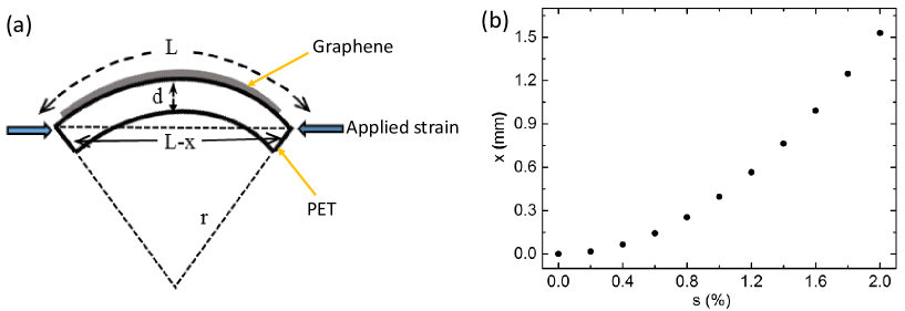
Tensile strain was applied to the graphene by bending the substrate, with graphene on the convex side, using a home-made micrometer-based mechanical device, similar to the the method used in Refs. MohiuddinPRB09 ; NiAM14 , as shown in Fig. 1 and Fig. 2. The nominal applied strain (assuming that graphene follows the substrate without slipping) is calculated as , where is the substrate thickness substrate and is the bending radius. Assuming a uniform bending, the micrometer displacement and the strain are related by the formula , where is the substrate width, as shown in Fig. 1(b). The same bending method was used in all measurements presented in this paper.
II.2 Experimental methods
The atomic force microscopy (AFM) and Kelvin probe force microscopy (KPFM) measurements were performed with Ti/Ir coated tips (resonance frequency 70 KHz) under controlled humidity (303%) at room temperature. These measurements proceed in two-pass scan mode: in the first pass, a normal topography height image is obtained in tapping mode; in the second pass, the cantilever is lifted 30 nm above the surface and follows the previously obtained topography to record the contact potential difference (CPD) between the graphene and the tip.
The Raman measurements were performed at the excitation wavelength of 514.5 nm (2.41 eV) with a 50 objective. The spot size was 1 m and the laser power less than 2 mW to avoid laser-induced heating. Due to the dominance of PET-induced Raman peaks over the phonon G peak of graphene (1580 cm-1), we have focused our analysis on the shift of the double-resonance 2D peak (2700 cm-1), which is moreover very sensitive to strain YuJPCCL08 ; MohiuddinPRB09 ; CorroJPC15 .
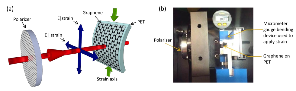
Infrared transmission spectra were measured using a standard FT–IR spectrometer (Bruker Vertex 70v) over the 40–700 cm-1 frequency range, using a globar light source and a liquid-He cooled Si bolometric detector. A spot size of 2 mm was used to keep light well in the middle of the sample. Absolute transmission at every strain value was normalized against the empty sample holder at the same micrometer position in order to keep the measurement conditions exactly the same. Spectra for both graphene/PET samples, and bare reference substrates were obtained separately for incident light polarized parallel () and perpendicular (E⟂) to the strain direction as sketched in Fig. 2.
All measurements were performed at room temperature. They were repeated during several strain cycles and showed excellent reproducibility.
III Results and discussion
III.1 Scanning probe and Raman measurements
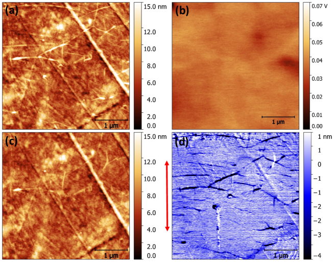
In Fig. 3(a) and (b) we show a typical a 44 m2 topographical micrograph and contact potential difference map renormalized around the mean value of the same region of unstrained graphene. The topography, representative of measurements performed at multiple different locations on the sample, reveals a clean graphene surface almost free from chemical residues, and is characterized by wrinkles and folds of different heights and orientations. For the CPD, while absolute values could not be determined in the absence of a reference calibration, we note that only very small variations are observed across the graphene surface, with a root mean square () value of 3.4 mV, which is limited by the resolution of KPFM setup at ambient conditions. When the same area is measured under higher nominal strain ( =1.2, 1.6 and 2%) no significant evolution of the values is observed. However, as can be seen in Fig. 3(c) for the topographical micrograph at 2% nominal strain, a number of small folds and wrinkles in the graphene appear to have relaxed. To quantify this relaxation behavior, we performed a differential analysis of the topographical images using an in-house developed drift correction algorithm Gaponenko_ms , which allows changes from one scan to another of the same area to be determined with sub-nm precision. Fig. 3(d) shows the resulting differential image, with the dark contrast features corresponding to all the wrinkles and folds that relaxed after the application of 2% nominal strain. They show decreased height with respect to the unstrained graphene imaged in Fig. 3(a). We can see that relaxation occurs primarily for wrinkles aligned perpendicular to the axis of applied strain, indicated by the red arrow, as would be logically expected. The only clear increase in the height of a fold, occurring in the star-like feature at the upper right of the image, was observed for a wrinkle aligned parallel to the the axis of applied strain, and accompanied relaxation in the rest of the feature. These strong variations of the nanoscale topographic landscape through relaxation under the applied strain imply that the effective strain transferred to the sample might be significantly smaller than the nominal strain.
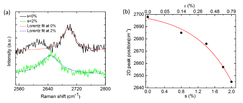
The actual amount of strain applied to graphene was therefore calibrated with Raman measurements. At 2% nominal strain, we observed a 52 cm-1 red shift caused by the elongation and weakening of C-C bonds, displacing the 2D peak from 2697 to 2645 cm-1 as shown in Fig. 4(a). The solid black and green lines show the experimental data measured at 0% and 2% nominal strain, respectively, fitted with a Lorentzian function (red dashed line for 0% and blue dashed line for 2%). The observed red shift in the position of the 2D peak is smaller than the values of 64 cm-1 per % uniaxial strain reported by Mohiuddin , on a mechanically exfoliated single layer graphene flake free of wrinkles and grain boundaries associated with CVD-grown material MohiuddinPRB09 . In our case, we must therefore presume that the observed relaxation of folds/wrinkles leads to a sliding at the graphene-PET interface HeAPL15 , and use the single-grain data as a reference to calibrate the effective vs. nominal strain in our measurements. Fig. 4(b) shows the 2D peak position (black circles) as a function of nominal strain (bottom abscissa) and the corresponding effective strain (upper abscissa). The corresponding values of the red shift were extracted from a fit of the data (red line). is then obtained using the relation cm-1 per % uniaxial strain, based on the exfoliated graphene results MohiuddinPRB09 .
III.2 Far-infrared measurements
As the PET substrate demonstrates strong photoelastic effects (as discussed in the Supplementary Information) it is necessary to fully characterize it optically as a function of the bending radius before the extraction of the intrinsic graphene properties. To this end we used a reference graphene-free substrate of the identical thickness, taken from the same batch. In Fig. 5 the absolute far-infrared transmission spectra are presented for the polarization of light parallel (a) and perpendicular (b) to the strain axis. The spectra for a perfectly flat and a maximally bent substrate substrate, corresponding to the effective graphene strain of 0.79%, are shown by the dashed blue and green lines, respectively. One can see that the substrate is sufficiently transparent everywhere except in the region between 300 cm-1 and 540 cm-1, where strong phonon absorption is present. The observed minima at 138 cm-1 and 632 cm-1 are due to weaker optical phonons in PET, which do not fully block the transmission. Periodic oscillations due to the Fabry-Perot interference in the substrate are seen, as expected, in the spectral regions of high transparency. For both polarizations, applying strain results in a frequency-dependent reduction of the transmission due to the above-mentioned photoelastic effects. Applying a Kramers-Kronig analysis KuzmenkoRSI05 to these data allows us to extract the spectra of the complex refractive index for each polarization, at each value of the applied strain, as detailed in the Supplementary information.
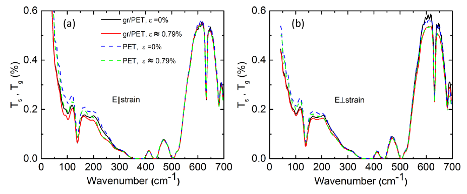
The solid black and red solid curves in Fig. 5 represent the absolute transmission of graphene on PET for zero and the highest effective strain (0.79%), respectively. The presence of the graphene monolayer noticeably reduces the transmission at low frequencies (below 200–300 cm-1) with respect to the bare substrate, while it does not essentially affect the transmission at high frequencies. Qualitatively, this indicates that the transmission reduction is due to the absorption by Drude carriers in graphene, as observed previously HorngPRB11 ; KimAPL12 ; SensaleNatComm12 .
In order to see the Drude absorption more clearly, in Fig. 6 we plot the extinction spectra , where the effects of the substrate are largely suppressed as compared to the absolute transmission. Furthermore, in order to avoid any spurious effects originating from a possible light depolarization in the substrate, from this point on we discuss the polarization-averaged, instead of polarization-resolved, spectra. Fig. 6(a) shows the extinction at zero strain (solid blue line), where a pronounced Drude peak is seen, with the maximum extinction reaching about 25% at the lowest frequencies. For an ultrathin film on a substrate the extinction is given by:
| (1) |
where 377 is the vacuum impedance, is the two-dimensional optical conductivity of graphene and
| (2) |
The substrate factor reduces the extinction as compared to the case of free standing graphene, where it is equal to one, and adds some Fabry-Perot oscillations, clearly seen in the experiment. The Drude model for the optical conductivity reads as HorngPRB11 :
| (3) |
where is the Drude weight and is the scattering time. The red curve in Fig. 6(a) presents the best fit using the Eqs (2) and (3). One can see that overall the model works well: apart from perfectly reproducing the shape of the Drude peak, it also generates Fabry-Perot oscillations similar to the experimental curve. The amplitude of the oscillations is difficult to match using the model due to various dephasing effects in the substrate. Nevertheless, from this fit we can rather accurately extract the Drude parameters kps-1, and ps. We emphasize that the ability to measure and independently is one of the advantages of the infrared spectroscopy as compared to the DC transport measurements. Within the theory of non-interacting Dirac fermions AndoJPSJ02 , the Drude weight is determined solely by the Fermi level with respect to the Dirac point: , where is the reduced Planck constant and is the elementary charge. Therefore, this measurement allows us to determine the Fermi level meV and the scattering rate meV. By adopting a standard value for the Fermi velocity ms-1, we can estimate the electronic mobility cm2V-1s-1 and the carrier concentration cm-2. These quantities are consistent with typical values found in CVD graphene under ambient conditions KimAPL12 ; HorngPRB11 ; RenNL12 .
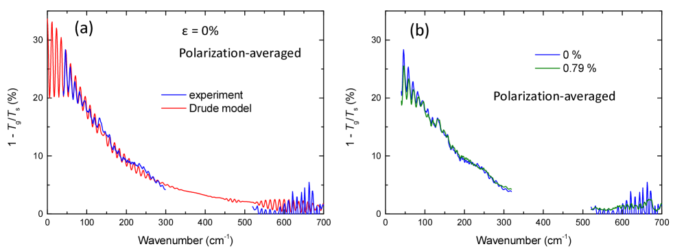
The effect of strain on the extinction spectra is shown in Fig. 6(b), where the blue and green curves correspond to =0% and 0.79%, respectively. One can see that the Drude peak somewhat flattens under strain, showing a smaller (higher) value below (above) 120 cm-1. This indicates that the scattering rate, which determines the width of the Drude peak, increases with strain, although a detailed analysis is required to quantify this effect, as carried out below. One can also notice that the amplitude of the Fabry-Perot oscillations at high frequencies decreases with strain, which is likely due to the substrate bending, not included in the flat-multilayer model, which may suppress the phase coherence between internally reflected rays.
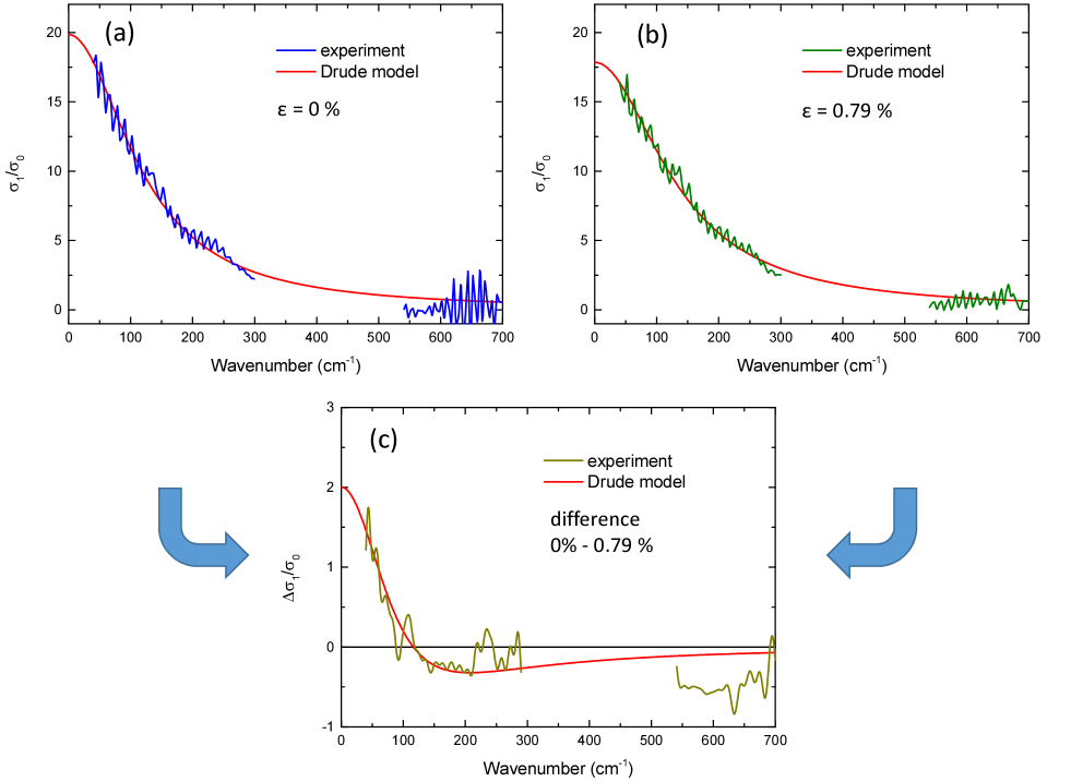
Before proceeding with a detailed analysis of the effect of strain, it is convenient to convert the extinction spectra into the optical conductivity of graphene using a model-independent Kramers-Kronig constrained analysis KuzmenkoRSI05 . Fig. 7(a) shows the extracted spectrum (blue line) as well as the best Drude fit (red line) of the real part of the optical conductivity, at zero strain, normalized to the universal value KuzmenkoPRL08 ; NairScience08 . The model matches the experiment well, apart from some remnant Fabry-Perot oscillations in the experimental curve, which appear due to the already-mentioned difficulty in precisely reproducing the oscillations in the extinction spectra. As one can see from Fig. 7(b), the Drude model works equally well at the maximum strain. The zero-frequency limit of the optical conductivity (obtained from the fit) shows a reduction from 20 to 18 , i.e. by about twice the total optical conductivity of graphene in the infrared and visible ranges KuzmenkoPRL08 ; NairScience08 . Thus the measured effect of strain on the optical conductivity in the far infrared regime is about two orders of magnitude larger than in the visible range NiAM14 . In order to emphasise the effect of strain, in Fig. 7(c) we plot the experimental frequency-dependent differential conductivity (dark yellow curve) and the corresponding difference between the Drude fits (red curve), where the remnant Fabry-Perot oscllations are Fourier-filtered. In spite of the unavoidable noise in the differential spectra, the match between experiment and the Drude model is obvious and a sign inversion is clearly observed at about 120 cm-1. This fully justifies our preliminary conclusion that the Drude peak broadens under strain.
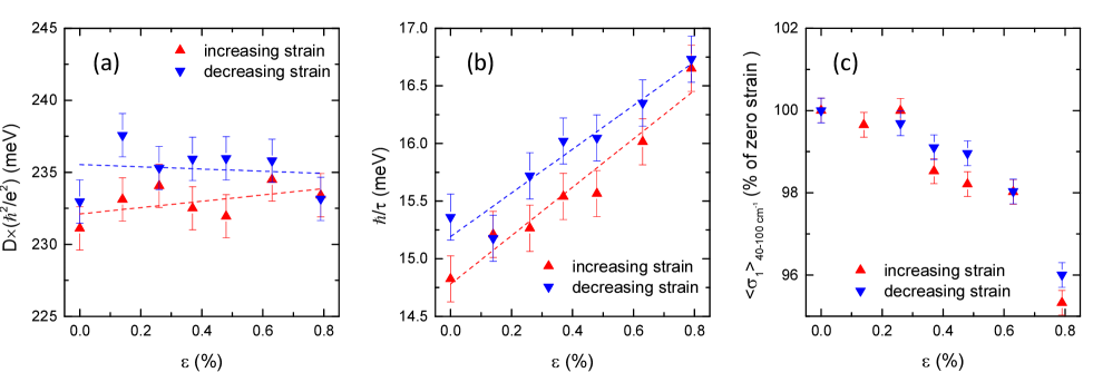
Using the same procedure, we extracted the Drude parameters independently at each value of strain. Furthermore, this was done separately for measurements carried out while increasing and decreasing the applied strain. Solid symbols in Fig. 8(a) and Fig. 8(b) show the Drude weight and the scattering rate , respectively, as a function of the effective strain for both phases of the cycle (red and blue). The dashed lines of the corresponding color are the linear fits. The central observation of this paper is that the Drude weight remains constant within the experimental error bars, while the scattering rate increases significantly with , by more than 10% at only 0.79% of strain. It is important to note that the behavior of both the Drude weight and the scattering rate is reproducible and reversible.
Fig. 8(c) shows the measured value of the optical conductivity, , normalized to zero strain and spectrally averaged between 40 and 100 cm-1 (1.2 - 3 THz), i.e. the part of the experimental range where the optical conductivity decreases most significantly with . One can see that the optical conductivity decreases reversibly by about 5% for the maximum applied strain, which is driven in the present case, as we have shown, by the strain dependent Drude scattering rather than the Drude weight.
III.3 Discussion of the Drude weight
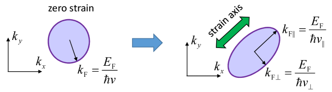
The effect of uniaxial strain on the crystal lattice and the electronic band structure of graphene was extensively studied theoretically LiuPRB07 ; PereiraPRB09 ; RibeiroNJP09 ; PellegrinoPRB10 ; PereiraEPL10 ; BaimovaPSS12 . The nearest neighbor hopping parameter for the -bands depends strongly on the bond distance : , where 3 eV and nm are the equilibrium values. Therefore, the major consequence of the lattice deformation is to modify the three effective hopping parameters and subsequently to shift and uniaxially deform each of the six Dirac cones located in the K-points of the Brillouin zone. This gives rise to elliptical Fermi pockets elongated along the strain axis, regardless of the direction of the strain with respect to the crystal axes PellegrinoPRB10 ; PereiraEPL10 (Fig.9). Thus, a uniaxial deformation is theoretically expected to anisotropically renormalize the Fermi velocity, producing two different values parallel () and perpendicular () to the strain, with . This also modifies the density of states at the Fermi level:
| (4) |
and makes the Drude weight anisotropic PellegrinoHPR10 :
| (5) |
Under small deformations, as in our experiment, we can apply a linear expansion for the strain-dependent Fermi energy:
| (6) |
and the (anisotropic) Fermi velocity:
| (7) |
where the index 0 refers to zero strain. As we show in the Supplementary Information, based on the existing ab-initio calculations RibeiroNJP09 , the Fermi-velocity expansion coefficients are equal to and and are independent of the strain orientation with respect to the crystal axis. This allows us to ignore the random orientation of the crystalline grains present in CVD graphene.
Using Equations (4)-(7), we can obtain a linear expansion for the density of states:
| (8) |
and the (anisotropic) Drude weight:
| (9) |
One can see that decreases, while increases with strain, which generates a Drude-weight dichroism determined solely by the anisotropy of the Fermi velocity and insensitive to the Fermi level. Measuring the anisotropy of the Drude weight would therefore directly probe the anisotropy of the Fermi velocity. Unfortunately, the photoelastic effects in the substrate did not allow us to measure the intrinsic dichroism of graphene with a sufficient precision, as discussed before. On the other hand, the average Drude weight is measured very accurately, since the substrate depolarization does not add to the total optical absorption. This value depends only on the shift of the Fermi energy and is not affected by the anisotropy. Therefore, our observation of a constant (within error bars) Drude weight (Fig. 8(a)) indicates that the Fermi level is essentially strain-independent: .
We note that this observation is a rather non-trivial one. Indeed, as the density of states varies with strain PereiraPRB09 ; PellegrinoPRB10 ; ShahMPLB13 ; HeAPL15 , one has to assume a strain-induced charge transfer between graphene and the environment (in particular, the substrate) in order to maintain constant. It is therefore likely that the PET substrate acts as a charge reservoir maintaining the chemical potential in graphene at a fixed level. Interestingly, our KPFM experiments show a rather small spatial variation of the chemical potential (about 3.4 meV), which may be also due to the stabilizing effect of the substrate on the chemical potential.
III.4 Discussion of the strain-dependent scattering rate
Next we discuss the surprisingly strong strain-induced increase of the scattering rate shown in Fig. 8(b). The data are well described by a linear dependence (dashed lines):
| (10) |
where the values and are found for the increasing and decreasing strain respectively. By taking the average value, we obtain the linear expansion coefficient . Speaking differently, the scattering rate increases by about 13.5 % per 1% of the applied strain, which indicates that the Drude scattering is highly sensitive to the mechanical deformation.
In a recent theoretical report ShahMPLB13 , the effect of strain-dependent density of states on the scattering rate was calculated in a connection to transport measurements, and a significant increase of with increasing strain was found. While the predicted effect was characterized as giant, the results of Ref. ShahMPLB13 are in fact smaller than what we observe here.
As it is widely discussed in the literature AndoJPSJ06 ; TanPRL07 ; HwangPRL07 ; StauberPRB07 ; ChenNP08 ; HwangPRB08 ; PonomarenkoPRL09 ; HwangPRB13 ; SongSR12 ; ShahMPLB13 ; YuPRB16 , the charge scattering in graphene is affected by short-range point defects (pd), long-range charged impurities (ci), acoustic phonons (ap), surface-phonons (sp) in the substrate, and the graphene grain boundaries. According to the Matthiessen’s rule, the total scattering rate is a sum of these respective contributions: . In principle, each of them may contribute to the total strain dependence. We can therefore attribute to each scattering channel () its respective strain-induced increase rate :
| (11) |
Even though we cannot distinguish the different scattering-rate contributions experimentally, it is clear that , i.e. there should be at least one scattering channel, for which . In the following discussion, we therefore consider each mechanism separately in order to identify candidate channels responsible for the large effect observed here. As we analyze the polarization-averaged spectra, and in order to use the existing theoretical literature, where only the isotropic case was considered, we neglect the strain-induce anisotropy of the Fermi surface and assume that the density of states changes with strain according to Eq. (8), where we furthermore set , in agreement with our experiment.
Point defects. Point defects are assumed to be uncharged short-range scatterers with a potential and the concentration located directly in the graphene plane. They contribute to the scattering rate as follows HwangPRL07 ; StauberPRB07 :
| (12) |
As the density of defects per unit cell remains the same, the spatial density changes inversely with the area of the unit cell, leading to , where we ignore a small Poisson ratio (0.16 in graphite BlaksleeJAP70 ; PereiraPRB09 but possibly even smaller in graphene on a substrate). Assuming that does not change, we obtain:
| (13) |
where is the average Fermi-velocity expansion coefficient. Such a small theoretical value of allows us to safely exclude point defects as a candidate mechanism.
Charged impurities. The scattering potential of charged impurities is given by: , where is the average dielectric constant of the media surrounding the graphene and is the distance between the layer containing these impurities (typically the substrate) and the graphene sheet HwangPRL07 ; StauberPRB07 . The contribution of charged impurities to scattering, which takes into account a dynamical self-screening by the graphene electrons, can be expressed as follows AndoJPSJ06 ; HwangPRL07 ; StauberPRB07 (see the Supplementary Information):
| (14) |
Here is the impurity concentration, is the Fermi momentum and is the effective graphene fine-structure constant.
One can see that multiple parameters affect , contributing rather differently to its strain dependence. First, the density of states , which is now in the denominator, tends to decrease the scattering rate, in contrast to the case of point defects. Second, applying strain increases, peculiarly, the graphene fine-structure constant via a reduced Fermi velocity: . From Eq. (14) it follows that increasing leads to the growth of the scattering rate. Third, the scattering rate is affected by the graphene-impurity distance and by the Fermi momentum via their dimensionless product . As the Fermi energy is fixed, the Fermi momentum increases with strain: , which reduces scattering. However, if decreases with strain, this may potentially increase of . Since we apply strain by bending the PET substrate, it is possible that this brings the graphene closer to the substrate (where we assume the charged scatterers are located). If nm then 1, which a regime where the scattering is highly sensitive to the graphene-substrate separation HwangPRL07 .
By combining these competing factors, we obtain:
| (15) |
where is the integral in the Eq. (14) and . Specifically, assuming that , we numerically obtain . One can see that the total contribution of other factors than the distance would result in the opposite strain dependence as compared to the experiment. Thus only the change of may account for the effect that we observe. Specifically, if , i.e. decreases by more than 8% at 1% of applied strain, then , which would quantitatively explain our experimental observation. Although we cannot measure and directly, these estimates do not seem to be unreasonable, given that CVD graphene is bound very weakly to the substrate. Consequently, we speculate that the increase of scattering by charged impurities due to the reduction of the effective graphene-PET distance might be an explanation of our experimental observation.
Acoustic phonons. Scattering from the acoustic phonons was calculated in StauberPRB07 ; HwangPRB08 :
| (16) |
where is the mass density, is the sound velocity (averaged over the longitudinal and transverse branches), is the deformation potential, and is the Boltzmann constant. When strain is applied, both the mass density and the sound velocity decrease: and . Based on theoretical results of Ref.BaimovaPSS12 , we can estimate that . Ignoring a possible strain-induced decrease of the deformation potential, we obtain:
| (17) |
Since is well below the experimental value of 13.4, one can also exclude the acoustic phonons as a dominant contribution to the strain-induced increase of the total scattering rate.
Surface phonons. At room temperature, surface optical phonons in polar substrates such as SiO2 and SiC also contribute to scattering in the overlying graphene HwangPRB13 . We are not aware whether or not this mechanism is at work for a polymer substrate like ours. The analytical formula for is too complicated to be presented here. Importantly, however, the dynamical screening gives rise to a strong dependence of the surface-phonon scattering on the distance , similar to the case of charge impurities. Thus, the effect of the surface phonons cannot be excluded at the moment as a candidate for the strain-induced increase of .
Grain boundaries. In CVD graphene, grain boundaries are known to diminish the effective transport mobility SongSR12 . The boundary region acts as a resistance in series with the bulk graphene, which can be expressed in terms of an additional scattering rate for the static conductivity. In optics, however, the situation is different. As the boundary regions represent a small fraction of the total graphene area, the effect of the boundaries is to excite graphene plasmons due to the breaking of translational symmetry, rather than to increase the Drude scattering rate. This would shift the Drude peak to finite energies CrasseeNL12 , which would produce a totally different spectral shape of the differential conductivity than what we observe in Fig. 7(c). Thus, we can exclude the grain boundaries from the candidate list.
III.5 Effect of strain on the charge mobility and electromagnetic absorption
Based on the observed growth of the scattering rate we can estimate its effect on other important parameters, such as the mobility and the terahertz/microwave absorption. If the Fermi level is fixed, the anisotropic mobility is determined by the anisotropic Fermi velocity and the scattering rate (which we assume to be isotropic):
| (18) |
from which it follows that
| (19) |
Using the experimentally obtained value of and theoretical values for we find that and should decrease with a rate of 17% and 12.5% per 1% of strain, respectively.
The (anisotropic) optical absorption in the low-THz and the microwave range, where , is proportional to the zero-frequency limit of the (anisotropic) optical conductivity:
| (20) |
which yields in the linear approximation:
| (21) |
Therefore and , and the corresponding low-frequency absorption coefficients should decrease with a rate of 15.7% and 11.1% per 1% of strain, respectively.
Although the strain value in our experiment was limited to about 0.8%, graphene can in principle support strains of up to 25% LiuPRB07 ; KimNature09 depending on the substrate used. The large numbers discussed above therefore suggest the possibility to controllably and reproducibly vary the mobility and optical absorption of graphene by several tens of percent, even if the linear dependence observed in our present study will eventually saturate.
IV Conclusion
We investigated the far-infrared optical conductivity of CVD-graphene on a flexible PET substrate under a tensile uniaxial strain, nominally up to 2%. These experiments were supported by AFM/KPFM measurements that revealed a flattening of wrinkles and folds initially present in graphene. Using Raman spectroscopy allowed us to calibrate the effective strain values, which was found to be smaller than the nominal strain, probably due to this wrinkle relaxation. Fitting the far-infrared spectra to the Drude model allowed us to accurately determine the Drude weight and the optical scattering rate independently as functions of the applied strain.
We find that the Drude weight remains essentially constant, implying that the Fermi level is quenched at a fixed level, probably by the presence of the substrate acting as a charge reservoir to compensate the strain-induced changes in the density of states of graphene. Additionally, we observe a strong linear increase of the scattering rate (by about 13% per 1% of the applied strain). This effect is found to be reversible and reproducible during strain cycling. A detailed theoretical analysis suggests that a likely origin of this unexpected effect is a change of the distance between graphene and the substrate, which influences, via a modified dynamical screening, the electronic scattering by the charged impurities or polar surface phonons in the substrate. In both cases, this mechanism would be truly unique for a 2D material, where the substrate plays a critical role.
Regardless of the actual physical mechanism, the strong effect of strain on the scattering rate may have important implications for graphene-based flexible optoelectronic devices, as it affects the electronic mobility and low-energy electromagnetic absorption. In particular, CVD graphene on plastic substrates is becoming increasingly important for flexible photodetectors, touch screens and microelectromechanical systems (MEMS). Our observation that these properties can be controlled mechanically, is therefore important for benchmarking and diversifying the functionalities of such devices.
V Acknowledgements
This research was supported by the EU Graphene Flagship (Contract No. CNECT-ICT-604391 and 696656) and by the Swiss National Science Foundation (Grants No. 200020-156615 and 200021-15317). PP and IG acknowledge UniGE COINF support allowing the development of the drift correction differential analysis algorithm. The authors are grateful to S. Muller, M. Brandt, J. Teyssier, J.-M. Poumirol and P. Tückmantel for discussions and technical assistance.
References
- (1) Bonaccorso F, Sun Z, Hasan T and Ferrari A C 2010 Graphene photonics and optoelectronics Nat. Photon. 4 611
- (2) Jang H, Park Y J, Chen X, Das T, Kim M S and Ahn J H 2016 Graphene-Based Flexible and Stretchable Electronics Adv. Mater. 28 4184
- (3) Lee C, Wei X, Kysar J W and Hone J 2008 Measurement of the Elastic Properties and Intrinsic Strength of Monolayer Graphene Science 321 385
- (4) Liu F, Ming P and Li J 2007 Ab initio calculation of ideal strength and phonon instability of graphene under tension Phys. Rev. B 76 064120
- (5) Kim K S 2009 Large-scale pattern growth of graphene films for stretchable transparent electrodes Nature 457 706
- (6) Shioya H, Russo S, Yamamoto M, Craciun M F and Tarucha S 2015 Electron states of Uniaxially Strained Graphene Nano Lett. 15 7943
- (7) He X 2015 Tuning the graphene work function by uniaxial strain Appl. Phys. Lett. 106 043106
- (8) Yu T, Ni Z, Du C, You Y, Wang Y and Shen Z 2008 Raman Mapping Investigation of Graphene on Transparent Flexible Substrate: The Strain Effect J. Phys. Chem. Lett. 112 12602
- (9) Mohiuddin T M G 2009 Uniaxial strain in graphene by Raman spectroscopy: G peak splitting, Gruneisen parameters and sample orientation Phys. Rev. B 79 205433
- (10) Corro E D, Kavan L, Kalbac M and Frank O 2015 Strain Assessment in Graphene through the Raman 2D mode J. Phys. Chem. C 119 25651
- (11) Ni G X, Yang H Z, Ji W, Baeck S J, Toh C T, Ahn J H, Pereira V M and Ozyilmaz B 2014 Tuning Optical Conductivity of Large-Scale CVD Graphene by Strain Engineering Adv. Mater. 26 1081
- (12) Pellegrino F M D, Angilella G G N and Pucci R 2010 Effect of uniaxial strain on the Drude weight of graphene High Pressure Res. 31 98
- (13) Pereira V M, Castro Neto A H and Peres N M R 2009 Tight-binding approach to uniaxial strain in graphene Phys. Rev. B 80 045401
- (14) Ribeiro R M, Pereira V M, Peres N M R, Briddon P R and Castro Neto A H 2009 Strained graphene: tight-binding and density functional calculations New J. Phys. 11 115002
- (15) Kim J Y, Lee C, Bae S, Kim S J, Kim K S, Hong B H and Choi E J 2012 Effect of uni-axial strain on THz/far-infrared response of graphene Appl. Phys. Lett. 100 041910
- (16) Gaponenko I, Tückmantel P, Ziegler B, Rapin G, Chhikara M and Paruch P Computer vision distortion correction of scanning probe microscopy images, submitted to Sci. Rep.
- (17) Kuzmenko A B 2005 Kramers–Kronig constrained variational analysis of optical spectra Rev. Sci. Instrum. 76 083108
- (18) Horng J 2011 Drude conductivity of Dirac fermions in graphene Phys. Rev. B 83 165113
- (19) Sensale-Rodriguez B, Yan R, Kelly M M, Fang T, Tahy K, Hwang W S, Jena D, Liu L and Xing H G 2012 Broadband graphene terahertz modulators enabled by intraband transitions Nat. Commun. 3 780
- (20) Ando T,Zheng Y and Suzuura H 2002 Dynamical Conductivity and Zero-Mode Anomaly in Honeycomb Lattices J. Phys. Soc. Jpn. 71 1318
- (21) Ren L 2012 Terahertz and Infrared Spectroscopy of Gated Large-Area Graphene Nano Lett. 12 3711
- (22) Kuzmenko A B, van Heumen E, Carbone F and van der Marel D 2008 Universal Optical Conductance of Graphite Phys. Rev. Lett. 100 117401
- (23) Nair R R, Blake P, Grigorenko A N, Novoselov K S, Booth T J, Stauber T, Peres N M R and Geim A K 2008 Fine Structure Constant Defines Visual Transparency of Graphene Science 320 1308
- (24) Pellegrino F M D, Angilella G G N and Pucci R 2010 Strain effect on the optical conductivity of graphene Phys. Rev. B 81 035411
- (25) Pereira V M, Ribeiro R M, Peres N M R and Castro Neto A H 2010 Optical properties of strained graphene EPL 92 67001
- (26) Baimova Y A, Dmitriev S V, Savin A V, and Kivshar Y S 2012 Velocities of sound and the densities of phonon states in a uniformly strained flat graphene Sheet Phys. Solid State 54 866
- (27) Shah R, Mohiuddin T M G and Singh R N 2013 Giant Reduction of Charge Mobility in Strained Graphene Mod. Phys. Lett. B 27 1350021
- (28) Ando T 2006 Screening Effect and Impurity Scattering in Monolayer Graphene J. Phys. Soc. Jpn. 75 074716
- (29) Tan Y W, Zhang Y, Bolotin K, Zhao Y, Adam S, Hwang E H, Das Sarma S, Stormer H L and Kim P 2007 Measurement of Scattering Rate and Minimum Conductivity in Graphene, Phys. Rev. Lett. 99 246803
- (30) Hwang E H, Adam S, and Das Sarma S 2007 Carrier Transport in Two-Dimensional Graphene Layers Phys. Rev. Lett. 98 186806
- (31) Stauber T, Peres N M R and Guinea F 2007 Electronic transport in graphene: A semiclassical approach including midgap states Phys. Rev. B 76 205423
- (32) Chen J H, Jang C, Adam S, Fuhrer M S, Williams E D and Ishigami M 2008 Charged-impurity scattering in graphene Nat. Phys. 4 377
- (33) Hwang E H and Das Sarma S 2008 Acoustic phonon scattering limited carrier mobility in two-dimensional extrinsic graphene Phys. Rev. B 77 115449
- (34) Ponomarenko L A 2009 Effect of a High-k Environment on Charge Carrier Mobility in Graphene Phys. Rev. Lett. 102 206603
- (35) Song H S, Li S L, Miyazaki H, Sato S, Hayashi K, Yamada A, Yokoyama N and Tsukagoshi K 2012 Origin of the relatively low transport mobility of graphene grown through chemical vapor deposition Sci. Rep. 2 337
- (36) Hwang E H and Das Sarma S 2013 Surface polar optical phonon interaction induced many-body effects and hot-electron relaxation in graphene Phys. Rev. B 87 115432
- (37) Yu K, Kim J, Kim J Y, Lee W, Hwang J Y, Hwang E H and Choi E J 2016 Infrared spectroscopic study of carrier scattering in gated CVD graphene Phys. Rev. B 94 235404
- (38) Blakslee O L, Proctor D G, Seldin E J, Spence G B and Weng T 1970 Elastic Constants of Compression-Annealed Pyrolytic Graphite J. Appl. Phys. 41 3373
- (39) Crassee I, Orlita M, Potemski M, Walter A L, Ostler M, Seyller Th, Gaponenko I, Chen I and Kuzmenko AB 2012 Intrinsic Terahertz Plasmons and Magnetoplasmons in Large Scale Monolayer Graphene Nano Lett. 12 2470