Latent Room-Temperature Tc in Cuprate Superconductors
Abstract
The ancient phrase, “All roads lead to Rome” applies to Chemistry and Physics. Both are highly evolved sciences, with their own history, traditions, language, and approaches to problems. Despite all these differences, these two roads generally lead to the same place. For high temperature cuprate superconductors however, the Chemistry and Physics roads do not meet or even come close to each other. In this paper, we analyze the physics and chemistry approaches to the doped electronic structure of cuprates and find the chemistry doped hole (out-of-the-CuO2-planes) leads to explanations of a vast array of normal state cuprate phenomenology using simple counting arguments. The chemistry picture suggests that phonons are responsible for superconductivity in cuprates. We identify the important phonon modes, and show that the observed K, the -dome as a function of hole doping, the change in as a function of the number of CuO2 layers per unit cell, the lack of an isotope effect at optimal doping, and the D-wave symmetry of the superconducting Cooper pair wavefunction are all explained by the chemistry picture. Finally, we show that “crowding” the dopants in cuprates leads to a pair wavefunction with S-wave symmetry and K. Hence, we believe there is enormous “latent” remaining in the cuprate class of superconductors.
The highest superconducting transition temperature, , at ambient pressure is 138 K in the Mercury cuprate HgBa2Ca2Cu3O8+δ (Hg1223) with three CuO2 layers per unit cell.Schilling1993 ; Mukuda2012 Hg1223 was discovered in 1993. The longest time period between record setting discoveries is the 17 years between Pb (1913 with K) to Nb (1930 with K). With the enormous increase in focus on superconductivity after the discovery of cuprates 30 years ago, the current 24 years without a new record at ambient pressure indicates we may be reaching the maximum attainable .
In this paper, we show this conclusion to be wrong. We demonstrate that can be raised above room-temperature to K in cuprates by precise control of the spatial separation of dopants. Hence, there still remains substantial “latent” in cuprates. Our proposed doping strategy and superconducting mechanism is not restricted to cuprates and may be exploited in other materials.
Our room-temperature result is based upon four observations:
-
•
Cuprates are intrinsically inhomogeneous on the atomic-scale and are comprised of insulating and metallic regions. The metallic region is formed by doping the material.
-
•
A diverse set of normal state properties are explained solely from the topological properties of these two regions and their doping evolution.
-
•
Superconductivity results from phonons at or adjacent to the interface between the metallic and insulating regions. Transition temperatures K are possible because the electron-phonon coupling is of longer-range than metals (nearest neighbor).
-
•
These interface phonons explain the observed superconducting properties and lead to our prediction of room-temperature superconductivity.
How is our claim of room-temperature possible? The talent and funding invested into finding the mechanism of cuprate superconductivity and higher materials has led to more than 200,000 refereed papers.Mann2011 After this mind-boggling quantity of literature, it seems unlikely that any unturned stones remain that could lead to our prediction.
Our claim does not come from locating an overlooked stone beneath the cuprate stampede. Instead, we believe the majority of the cuprate community settled upon the incorrect orbital nature of the doped hole. This mistake led to Hamiltonians (Hubbard models) that “threw the baby out with the bath water.”
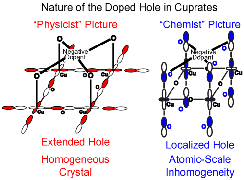
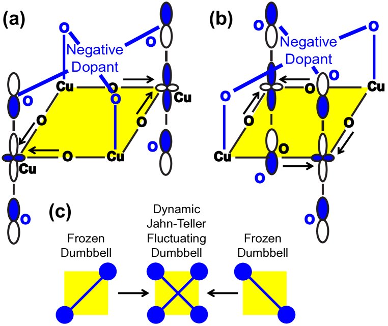
A major reason for the early adoption of these Hubbard models for cuprates was due to computational results using the ab initio local density approximation (LDA) in density functional theory (DFT). While LDA is now deprecated, being replaced by the Perdew-Burke-Ernzerhof functionalPBE (PBE), both functionals lead to exactly the same doped hole wavefunction in cuprates. These “physicist” functionals find the doped hole to be a delocalized wavefunction comprised of orbitals residing in the CuO2 planes common to all cuprates.Yu1987 ; Mattheiss1987 ; Pickett1989 Unfortunately, LDA and PBE both contain unphysical Coulomb repulsion of an electron with itself.Perdew1981 The “chemist” hybrid density functionals, invented in 1993 (seven years after the discovery of cuprate superconductivity), corrected for this self-Coulomb error, and thereby found the doped hole residing in a localized wavefunction surrounding the dopant atom with orbital character pointing out of the CuO2 planes.Perry2001 ; Perry2002 The physicist and chemist doped holes are shown in Figure 1. A discussion of the superiority of the chemist’s DFT to the physicist’s DFT is in Appendix A.
The “chemist’s” ab initio doped hole leads to eight electronic structure concepts that explain a vast array of normal and superconducting state phenomenlogy using simple counting. These eight structural concepts are described below.
Structural Concept 1: Cuprates are inhomogeneous on an atomic-scale. The inhomogeneity is not a small perturbation to translational symmetry. It must be included at zeroth order.
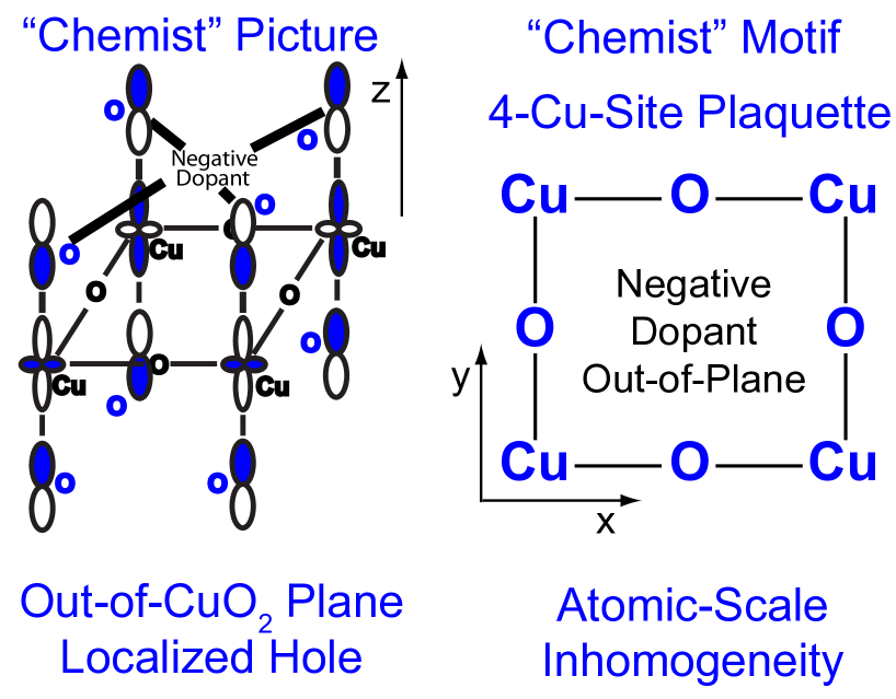
Structural Concept 2: The Cuprate motif is a four-Cu-site plaquette formed by each dopant. See Figure 2. The out-of-the-CuO2 plane negative dopant is surrounded by an out-of-the-CuO2 plane hole. The hole is comprised of apical Oxygen and planar Cu character. There is also some planar O character that is not drawn.
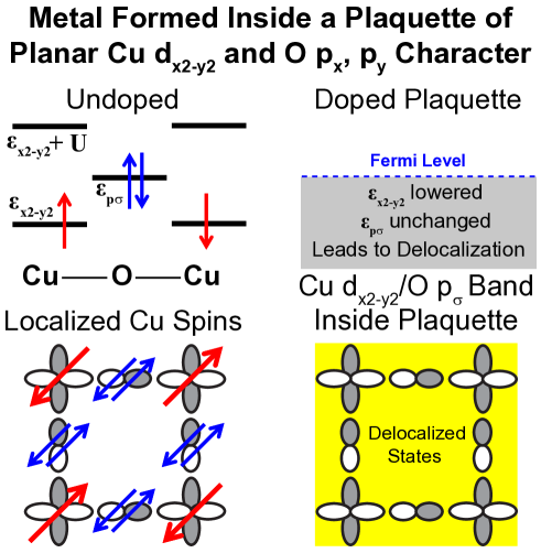
Structural Concept 3: A tiny piece of metal is formed within each plaquette from electron delocalization in the planar Cu and O ( and ) orbitals. See Figure 3. Delocalization occurs because the positive charge of the out-of-plane hole lowers the Cu orbital energy relative to the O orbital energy. In contrast, these electrons are localized in a spin-1/2 antiferromagnetic (AF) state in an undoped plaquette.
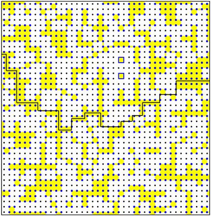
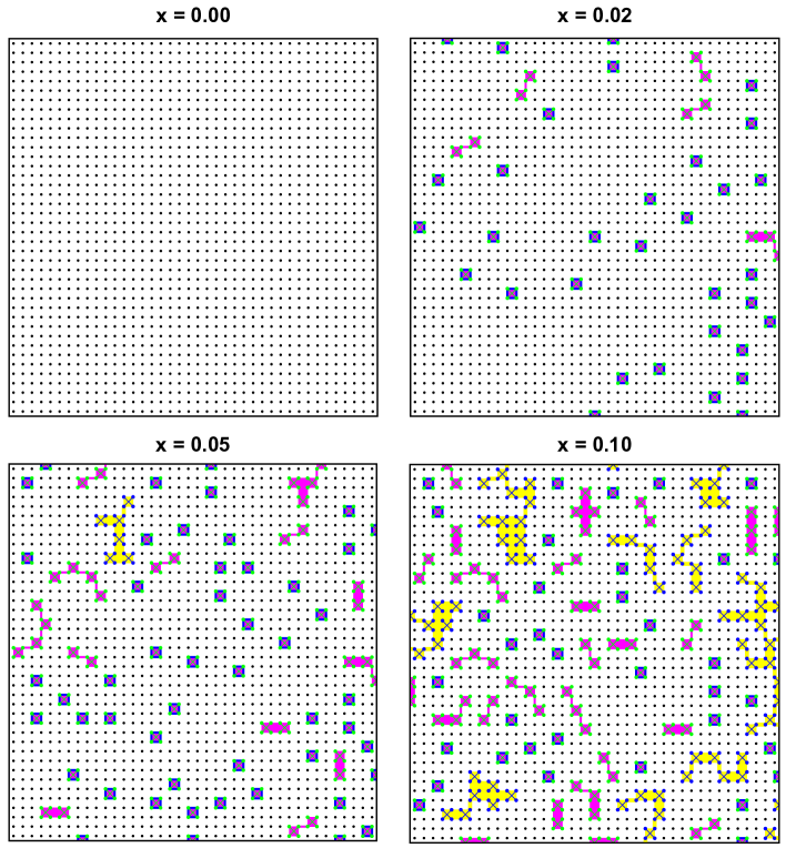
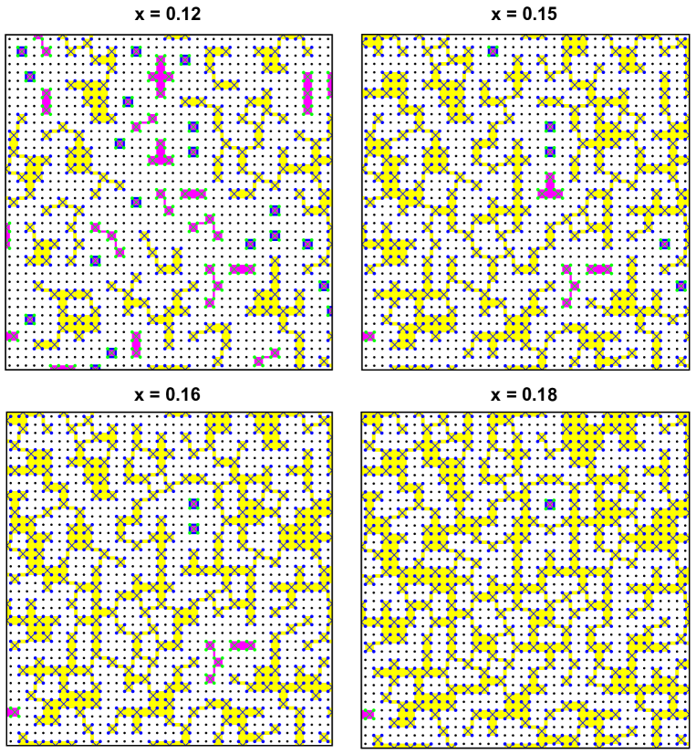
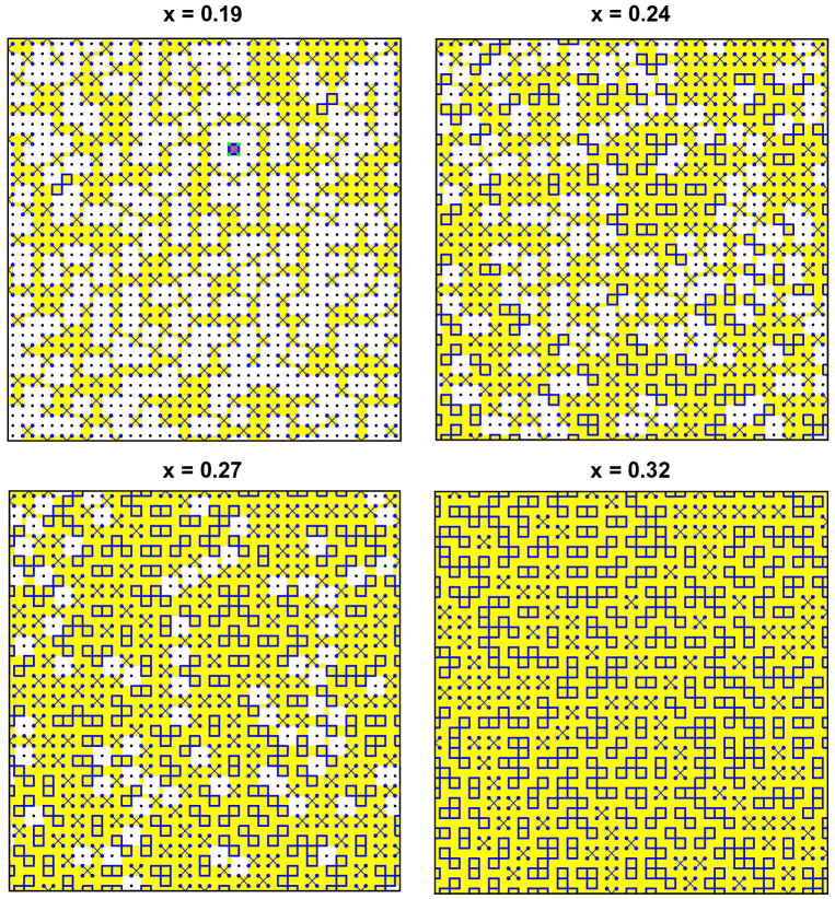
Structural Concept 4: A metal is formed when the doped plaquettes percolate through the crystal. When a three-dimensional (3D) pathway of adjacent doped plaquettes is created through the crystal (percolation of the plaquettes), a metallic band comprised of planar Cu and O orbitals is created inside the percolating region. These delocalized metallic wavefunctions do not have momentum, , as a good quantum number. Two-dimensional (2D) percolation occurs at a higher doping ( holes per planar Cu) than the start of 3D percolation (at holes per planar Cu). See Figure 4. The undoped (non-metallic) region remains an insulating spin-1/2 AF. Thus cuprates have both insulating and metallic regions on an atomic-scale.
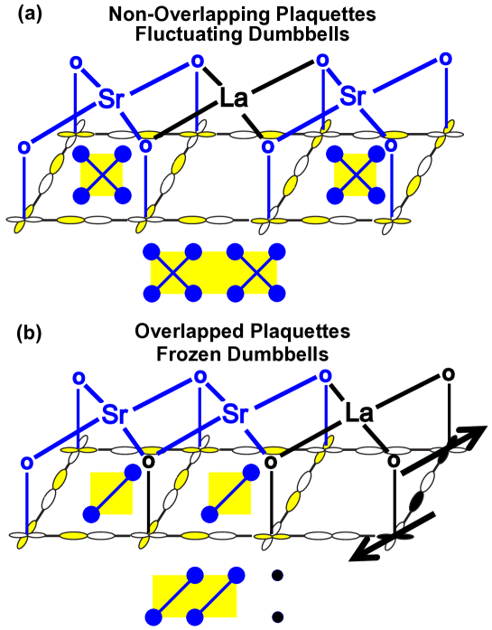
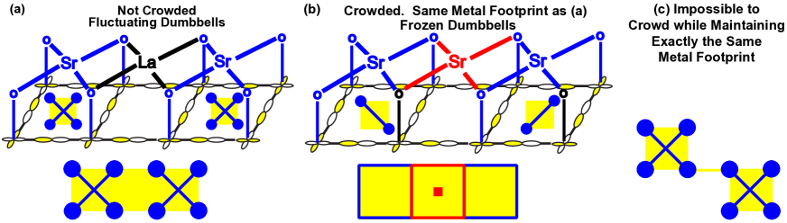
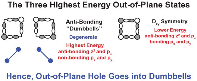
Structural Concept 5: The out-of-the-CuO2 plane hole shown in Figures 1 and 2 is a dynamic Jahn-Teller distortion that is a linear superposition of two “frozen dumbbell” states. See Figure 5. Figure 25 in Appendix C shows that the out-of-the-plane hole goes into the states in Figure 5. We call the dynamic Jahn-Teller hole state a “fluctuating dumbbell.”
Structural Concept 6: A fluctuating dumbbell can be frozen by overlapping its plaquette with another plaquette. See Figure 6.
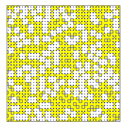
Structural Concept 7: If possible, plaquettes avoid overlapping. Since the dopant atom is negatively charged, two plaquettes will repel each other. Their Coulomb repulsion is short-ranged because of screening from the planar metallic electrons. Hence, plaquettes do not overlap, but are otherwise distributed randomly. Plaquettes can avoid overlap up to a hole doping of . For dopings greater than , plaquettes must overlap. Plaquettes overlap as little as possible to minimize their mutual repulsion. Up to doping, there always exists a four-site square of AF spins where the next plaquette can be placed. For the doping range , added plaquettes can cover three AF spins. In the range , plaquettes cover two AF spins, and from , a single localized spin. At , the crystal is fully metallic with no localized spins. Further doping cannot increase the number of metallic sites. Figure 4 shows that plaquettes can avoid overlap at doping. Figure 7 below shows doping, where plaquettes must overlap.
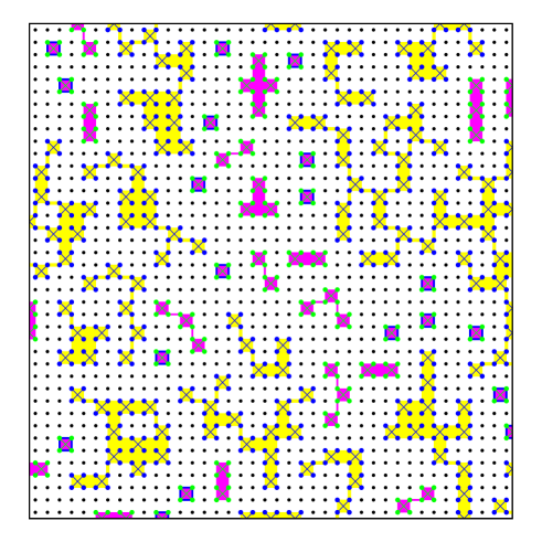
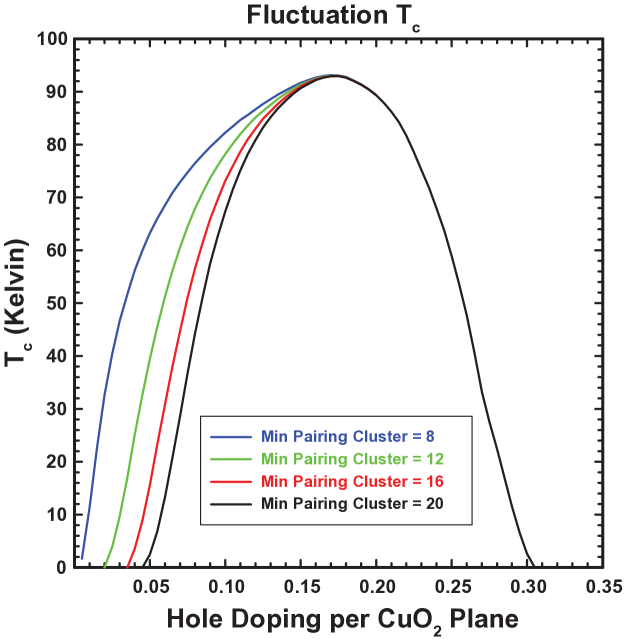
Structural Concept 8: Plaquette Clusters smaller than the superconducting coherence length ( nm) thermally fluctuate and do not contribute to the superconducting pairing. At low dopings, the plaquettes have not yet merged into a single connected region. There exist plaquette clusters smaller than the coherence length, as shown in magenta in Figure 8. They cannot contribute to the superconducting . These fluctuating clusters lead to superconducting fluctuations above .
Figures 9, 10, and 11 show the evolution of the plaquettes as a function of doping. Only twelve dopings are shown here from the range to . The Appendix has similar figures for all dopings in this range in increments (Figures S0S32). Only one CuO2 plane is shown in each of these figures.
The above eight electronic structural concepts explain a diverse set of normal state cuprate phenomenology as a function of doping by simple counting arguments,Tahir-Kheli2015 ; Tahir-Kheli2013 ; Tahir-Kheli2011 ; Tahir-Kheli2010 as we have shown previously. These include (See reference Tahir-Kheli2015, for a videotaped seminar summarizing all of these results.):
-
•
the low and high-temperature normal state resistivity by counting the number of overlapped plaquettes and the size of the metallic region.Tahir-Kheli2015 ; Tahir-Kheli2013
For La2-xSrxCuO4, the fluctuating dumbbells in adjacent CuO2 layers become decorrelated above K. Phonon modes with character predominantly inside these plaquettes become 2D, leading to the low-temperature linear resistivity term. For the double-chain cuprate, YBa2Cu4O8, if the fluctuating dumbbells between adjacent CuO2 layers are correlated, then these phonons remain 3D, leading to a low-temperature resistivity that is quadratic in temperature, as observed.Proust2016
-
•
the pseudogap and its vanishing at doping from counting isolated plaquettes (not adjacent to another doped plaquette in the same CuO2 plane) and their spatial distribution.Tahir-Kheli2015 ; Tahir-Kheli2011
As discussed in Appendix B, there is a degeneracy near the Fermi level of the planar states inside an isolated plaquette. The degeneracy is broken by interaction with the environment. A nearby isolated plaquette strongly splits the degeneracy and leads to the pseudogap.
-
•
the “universal” room-temperature thermopower by counting the sizes of the insulating AF and metallic regions and taking the weighted average of the thermopower of each region.Tahir-Kheli2015 ; Tahir-Kheli2010
Since the room-temperature thermopower of the AF region is and the metallic region thermopower is , there is a rapid decrease in the thermopower as the size of the metallic region increases with doping.
-
•
the STM doping incommensurability by counting the size of the metallic regions.Tahir-Kheli2015 ; Tahir-Kheli2010
-
•
the energy of the neutron spin scattering resonance peak by counting the size of the AF regions.Tahir-Kheli2015 ; Tahir-Kheli2010 The resonance peak arises from the finite spin correlation length of the AF regions.
In this paper, we use exactly the same doped electronic structure described above to explain the superconducting and its evolution with doping. We show that Oxygen atom phonon modes at and adjacent to the interface between the insulating and metallic regions lead to superconductivity. We estimate the magnitude of the electron-phonon coupling and obtain the following:
-
•
a large K from phonons (because the range of the electron-phonon coupling near the metal-insulator interface increases from poor metallic screening),
-
•
the observed -dome as a function of hole doping (since the total pairing is the product of the size of the metallic region times the interface size),
-
•
the large changes as a function of the number of CuO2 layers per unit cell (from inter-layer phonon coupling of the interface O atoms plus inhomogeneous hole doping of the layers),
-
•
the D-wave symmetry of the superconducting Cooper pair wavefunction (also known as the D-wave superconducting gap).
In general, an isotropic S-wave superconducting pair wavefunction is energetically favored over a D-wave pair wavefunction for phonon induced superconductivity. However, the fluctuating dumbbells reduce the S-wave below the D-wave by drastically increasing the Cooper pair electron repulsion.
-
•
the lack of a superconducting isotope effect at optimal doping (due to the random anharmonic potentials of each pairing O atom).
-
•
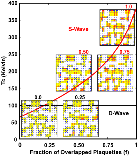
by overlapping plaquettes, the fluctuating dumbbells become frozen and the S-wave pair wavefunction rises above the D-wave . (Figure 19).
While maintaining the same metallic “footprint” of optimal doping (), completely frozen dumbbells lead to an S-wave of K when the D-wave K (Figure 19).
All the ’s in this paper are computed using the strong coupling Eliashberg equationsAllen1982 as detailed in Appendix G. These equations include the electron “lifetime” effects that substantially decrease from the simple BCS expression.
These results are shown in the following set of Concepts.
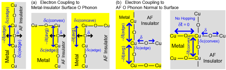
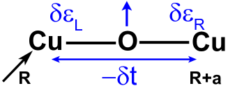
Concept 1: There are two planar O atom phonon modes (one at the metal-AF insulator interface and the other adjacent to the interface on the insulating side) that have longer-range electron coupling due to poor electron screening from the metallic region. See Figure 12. For the remainder of the paper, we use the “effective” single band model for the metallic band.Hashimoto2008 In this model, the planar O atoms are eliminated. The model has a single effective Cu orbital per Cu in the CuO2 plane with an effective hopping to neighboring metallic Cu atoms. The parameters of the band structure are the Cu orbital energy and the hopping terms (Table 2, Appendix F).
Concept 2: The typical magnitude of the electron-phonon coupling matrix element, , is the geometric meanAllen1982 of the Debye energy, , and the Fermi energy, , or . The derivation is given in Appendix D. For eV eV and eV, we find eV eV. All results in this paper use electron-phonon coupling parameters in this range.
Concept 3: The potential energy of each O atom in Figure 12 is strongly anharmonic due to the difference of the electron screening in the metallic and insulating regions. See Figure 13. In fact, the phonon mode shown in Figure 12a is anharmonic even without a nearby metal-insulator boundary. The “floppiness” of the bond-bending of a linear chain (here, the planar CuOCu chain) has been emphasized by Phillips,Phillips2007 and seen by neutron scattering (the F atomLi2011 in ScF3 and the Ag atomLan2014 in Ag2O). However, without the metal-insulator boundary, reflection symmetry would force the electron-phonon coupling for this mode to be zero.
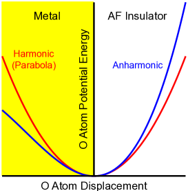
Concept 4: Near optimal doping, , there is no Tc isotope effect. Harmonic potentials have no isotope variation of the superconducting pairing strength because the pairing is inversely proportional to where is the O atom mass and is the angular frequency of the phonon mode. For a derivation of this result, substitute into the pairing coupling in Figure 14b, where is the electron potential. Since , where is the spring constant, there is no pairing isotope effect. For anharmonic potentials, the phonon pairing strength becomes dependent on the isotope mass.Hui1974 Anharmonic potentials can decrease or increase the isotope effect depending on the details of the anharmonicity.Crespi1991 ; Crespi1991a ; Crespi1993 Near optimal doping, the metallic and insulating environments for each O atom phonon is random, leading to an average isotope effect of zero, as observed.Keller2005 ; Keller2008 The O atom environment becomes less random at lower dopings, as seen in Figure 9. Hence, the isotope effect appears at low dopings.Keller2005 ; Keller2008
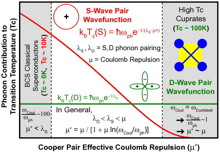
Concept 5: Cooper pairing from phonons is maximally phase coherent for an isotropic S-wave pair wavefunction because the sign of the pairing matrix element in Figure 14 is always negative. However, a D-wave pair wavefunction is observed for cuprates. It appears prima facie that phonons cannot be responsible for superconductivity in cuprates. Since Cooper pairs are comprised of two electrons in time-reversed states, the sign of the Cooper pair scattering is always negative and of the form ,deGennes-book ; Schrieffer-book where is the matrix element to emit a phonon and is the energy of the phonon mode. See Figure 14. Hence, the lowest energy superconducting pairing wavefunction is a linear superposition of Cooper pairs with the same sign. It is called the isotropic “S-wave” state. In theory, the pair Coulomb repulsion, , could suppress the S-wave state and lead to a D-wave state because cancels out of when performing the angular integral around the D-wave pair wavefunction. However, the electrons in a pair can couple via a phonon while avoiding each other (due to retardation of phonons). The “effective” repulsion, , known as the Morel-Anderson pseudopotentialBogoliubov-book ; Morel1962 ; deGennes-book ; Schrieffer-book ; Cohen1969 ; Allen1982 is too small to raise the D-wave higher than the S-wave . Unless there is a mechanism for drastically increasing , any phonon model for cuprate superconductivity is bound to fail to obtain the correct superconducting pair wavefunction. We show in Concept 6 that the fluctuating dumbbells in Figure 5 increase to , leading to a D-wave pairing wavefunction.
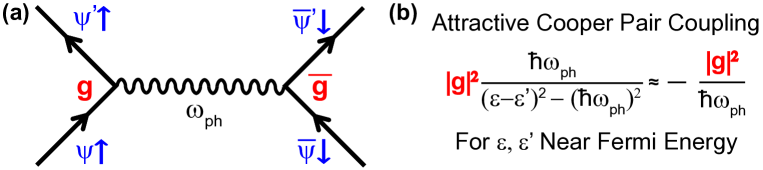
Concept 6: The fluctuating dumbbells suppress the S-wave pairing wavefunction and lead to a D-wave pairing wavefunction. See Figure 15. The expression for the Morel-Anderson Coulomb pseudopotential,Bogoliubov-book ; Morel1962 ; deGennes-book ; Schrieffer-book ; Cohen1969 ; Allen1982 , is shown in Figure 15. It depends on the ratio of the Coulomb and phonon energy scales, . Since this ratio is large, is small, leading to an S-wave pair wavefunction rather than the experimentally observed D-wave pair wavefunction.Tsuei2000 The fluctuating dumbbell frequency, , is of the same order as because of the dynamic Jahn-Teller distortion of the planar O atoms in Figure 5. The O atom distortion disrupts the metallic screening of the Coulomb repulsion, and thereby increases as shown in Figure 15. In essence, substitutes for in the expression for . When , a D-wave pair wavefunction is formed.
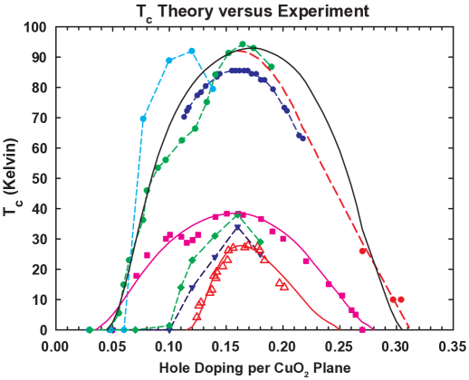
Concept 7: Interface O atom phonon pairing explains the experimental domes. Figure 16 shows the calculated -domes versus experiment as a function of doping for different cuprates using the phonon modes from Figure 12 and the electron-phonon couplings estimated in Concept 2. All three computed D-wave domes were obtained from the strong-coupling Eliashberg equations for .Allen1982 ; Schrieffer1963 ; Scalapino1966 Other phonon modes also contribute to . These phonons primarily reduce the magnitude of due to their contribution to electron pair “lifetime effects” (strictly speaking, the “ wavefunction renormalization effects”). The effect of all the phonon modes on are included in our computations. All the details of the band structure, the interface O phonon coupling parameters, and the inclusion of the remaining phonons into the Eliashberg calculations are described in appendices F and G. We intentionally chose our parameters to be simple and conceptual. We did not attempt to fit the experimental points exactly. Our goal is to demonstrate that reasonable electron-phonon couplings and our proposed inhomogeneous cuprate electronic structure are sufficient to understand the experimental -domes.
Concept 8: The experimental variation of with the number of CuO2 layers per unit cell is due to interlayer coupling of the interface O atom phonons and the nonuniform hole doping between layers. Since the O atom phonons near the metal-insulator interface are longer-ranged, they couple to adjacent CuO2 planes. Hence, there is a strong dependence of on the number of CuO2 layers per unit cell. In addition, the Cu Knight shift measurements of Mukuda et al.Mukuda2012 have shown that the hole doping is not the same in each CuO2 layer. The computed as a function of the number of CuO2 layers is shown in Figure 17.
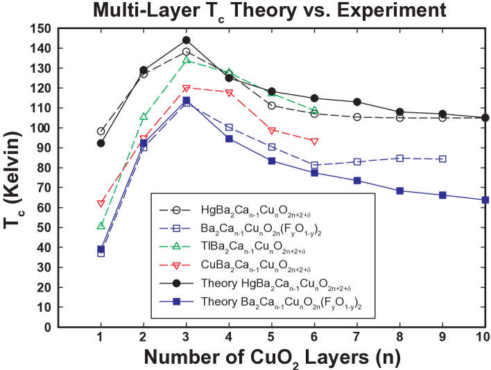
Concept 9: The D-wave Tc values computed in Figures 16 and 17 are weakly dependent on the orbital energy change, , and strongly dependent on the hopping energy change, . See Table 1 for the change in at optimal doping of for the computed black, red, and magenta curves in Figure 16.
| Change in | Black Curve | Magenta Curve | Red Curve |
|---|---|---|---|
| YBa2Cu3O7-δ | La2-xSrxCuO4 | YBa2(Cu0.94Zn0.06)3O7-δ | |
| 92.2 K | 38.5 K | 27.7 K | |
| 83.1 K | 30.7 K | 19.9 K | |
| 100.0 K | 46.3 K | 35.6 K | |
| 93.6 K | 39.4 K | 27.7 K | |
| 84.7 K | 31.3 K | 19.9 K | |
| 101.1 K | 47.5 K | 35.6 K | |
| 90.5 K | 37.5 K | 27.7 K | |
| 81.4 K | 30.1 K | 19.9 K | |
| 98.5 K | 45.0 K | 35.6 K |
From Table 1, a 10% increase in always decreases the D-wave by . A change in leads to change in the D-wave . In appendices G.2.1 and G.2.2, the exact dependence of the electron-phonon pairing parameter, , is derived. The contribution of to is approximately isotropic around the Fermi surface leading to a weak dependence of the D-wave on changes in . In contrast, an S-wave pairing symmetry depends strongly on both and . The weak dependence of the D-wave on implies our choices for the parameters for the curves in Figures 16 and 17 are not accurately fitted by the experimental data. The uncertainty in the magnitude of leads to an S-wave range from K due to dopant “crowding,” as shown next.
Concept 10: Overlapping plaquettes (“crowding” the dopants) freeze the dumbbells, decrease the Coulomb pseudopotential, , and thereby raise the S-wave Tc. If the same metallic “footprint” can be maintained, then there is no change in the phonon pairing. Only is reduced (see Figure 15). If all the dumbbells can be frozen, then from Figures 14 and 15, the S-wave will be larger than the D-wave . Figure 18 shows how two plaquettes with fluctuating dumbbells can be crowded by adding an additional dopant (Sr in the figure) while retaining exactly the same metallic footprint. For random doping, there will always exist adjacent plaquette pairs as shown in Figure 18c that cannot be overlapped by another plaquette within the existing metallic footprint. There are two ways to obtain an optimally doped metallic footprint and freeze 100% of the dumbbells. First, dope “dominoes” (adjacent pairs of plaquettes as in Figure 18a and b). Second, dope to less than optimum doping. Next, crowd all of the plaquettes in such a way as to end up with an optimally doped metallic footprint and 100% frozen dumbbells.
Concept 11: Crowding dopants while maintaining the optimal doping metallic footprint leads to room temperature S-wave . See Figure 19.
Cuprate Physics and Its Analogy to Chemical Dissociation
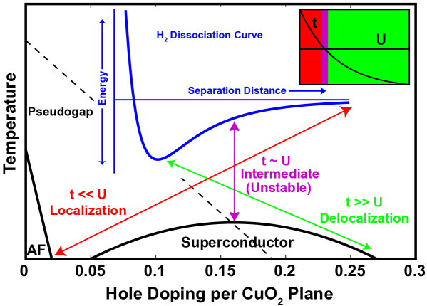
In Figure 20, the ground state electronic wavefunction of H2 at the equilibrium bond separation of 0.74 Å is well approximated by a restricted Hartree-Fock form (a spin up and spin down electron pair occupying the same bonding orbital). In the language of an effective electron hopping, , and an onsite Coulomb repulsion, , this region is represented by . At dissociation (), the ground state electronic wavefunction is highly correlated. The wavefunction is large only when there is one electron on each H atom.
From Figure 20, the optimal superconducting of cuprates is at “intermediate” correlation. Molecules do not generally “settle” at intermediate correlation. Since the dopants in cuprates are frozen in at high temperatures, the material avoids intermediate correlation by phase separating on an atomic-scale into a metallic (weak correlation) and an insulating AF (strong correlation) regions.
Atomic-scale inhomogeneity explains three important materials issues about cuprates. First, cuprates “self-dope” to approximately optimal . Since plaquette overlap occurs at doping, we believe it is energetically favorable for dopants to enter the crystal until their plaquettes begin to overlap. Adding further dopants is energetically unfavorable. The change in between optimal doping () and plaquette overlap () is . Hence, cuprates “self-dope” to approximately optimal as a consequence of the energetics of overlapping plaquettes.
Second, YBa2Cu3O7-δ cannot be doped past , as shown in Figure 16. The phenomenon can be understood if it is energetically unfavorable to overlap plaquettes that share an edge (occuring at doping ). In the earliest days of cuprate superconductivity, materials scientists had difficulty observing superconductivity in La2-xSrxCuO4 above doping.Takagi1989 We believe the difficulty was also due to the energetics of overlapping plaquettes with shared edges. Annealing in an O2 atmosphere solved the La2-xSrxCuO4 overdoping problem. However, the problem still remains for YBa2Cu3O7-δ.
Third, it is known that a room-temperature thermopower measurement is one of the fastest ways to determine if a cuprate sample is near optimal doping for because the room-temperature thermopower is very close to zero near optimal doping. This peculiar, but useful, observation can be understood because 2D percolation of the metallic region occurs at doping. Since the AF region thermopower is large ( and the metallic thermopower is at high overdoping, 2D metallic percolation “shorts out” the AF thermopower and drives the thermopower close to zero near optimal .
Finally, the potential energy curve in the intermediate correlation regime is hard to study for molecules. For H2, the equilibrium bond distance is 0.74 Å. The intermediate correlation regime is at Å bond separation. At this distance, the blue potential energy curve in Figure 20 can only be observed indirectlyHerzberg-vol1 ; Herzberg-vol2 ; Wilson-book because it is not at a local minimum. For H2, the ultraviolet spectrum of the vibrational modes (there are 14 discrete level below the continuum) can be fitted to a simple Morse potential to estimate the potential energy as a function of the separation distance. The bond-stretching phonon mode probes the potential energy of the two of H atoms up to Å.
Materials Approaches to Room-Temperature Tc and Large
There is enormous “latent” residing in the cuprate class of superconductors from converting the D-wave superconducting pairing wavefunction to an S-wave pairing wavefunction. The result is surprising because it has been assumed by most of the high- cuprate community, including the author, that there was something special about the D-wave pairing symmetry that led to K.
The first thought that comes to mind given our finding is, “With over 200,000 refereed papersMann2011 and 30 years of intensive research in both academia and industry, surely someone overlapped plaquettes, and thereby created a room-temperature S-wave superconductor?”
Our answer is that plaquettes have been overlapped with regularity for 30 years. These materials are all overdoped with doping , as shown in Figure 11. Hence, dumbbells have been frozen and the S-wave has increased. However, our calculations find the S-wave remains below the D-wave for reasonable parameter choices. Unfortunately, the optimally doped metallic footprint is not obtained by naive dopant crowding. Instead, the size of the metallic footprint increases and its pairing interface decreases. The right side of the -dome shown in Figure 16 is the result. Even the layer-by-layer Molecular Beam Epitaxy (MBE) of Bozovic et al.Pereiro2012 does not control the placement of the dopants in each layer, leading to the same result as above.
While almost everything that can be possibly be suggested for the mechanism for cuprate superconductivity has been suggested in over 200,000 papers (percolation, inhomogeneity, dynamic Jahn-Teller distortions, competing orders, quantum critical points at optimal doping or elsewhere, spin fluctuations, resonating valence bonds, gauge theories, blocked single electron interlayer hopping, stripes, mid-infrared scenarios, polarons, bipolarons, spin polarons, spin bipolarons, preformed Bose-Einstein pairs, spin bags, one-band Hubbard models, three-band Hubbard models, t-J models, t+U models, phonons, magnons, plasmons, anyons, Hidden Fermi liquids, Marginal Fermi liquids, Nearly Antiferromagnetic Fermi liquids, Gossamer Superconductivity, the Quantum Protectorate, etc.), we believe these ideas have lacked the microscopic detail necessary to guide experimental materials design, and in some instances, may have even led materials scientists down the wrong path.
We have shown above that freezing dumbbells in cuprates leads to room-temperature (see Figure 19). However, the critical current density, , is approximately two orders of magnitude smaller than the theoretical maximum, , where is the depairing limit for Cooper pairs. is small because the conducting pathway in the CuO2 planes is extremely tenuous (see the discussions in the captions of Figures 4 and 10). For practical engineering, should be at least .
In cuprates, can be raised to room-temperature by freezing dumbbells while maintaining the random metallic footprint found at optimal doping. By fabricating wires (a wire is defined as a continuous 1D metallic pathway through the crystal), remains large while increases to at least .
Our results lead to the following approaches for achieving higher and . Unless explicitly stated, the bullet points below apply to any type of material (cuprate or non-cuprate).
-
•
The material should be inhomogeneous with a metallic region and an insulating region.
The insulating region does not have to be magnetic. However, we believe the antiferromagnetic insulating region helps maintain the sharp metal-insulator boundary seen in cuprates. An ordinary insulator or a semiconductor with a small number of mobile carriers is sufficient to obtain a longer ranged electron-phonon coupling at the interface because there is less electron screening in the semiconducting (or insulating) region compared to the metallic region.
-
•
The ratio of the number of metallic unit cells on the interface (adjacent to at least one insulating unit cell) to the total number of metallic unit cells must be larger than 20%.
We use the terms interface and surface interchangeably below.
The number of metallic unit cells on the interface (or surface) must be a large fraction of the total number of metallic unit cells in order for the enhanced electron-phonon pairing at the interface to have an appreciable affect on . From our calculations in Figure 16, 50% of optimal is obtained when the ratio is , and 25% of optimal occurs when the ratio is . Below a surface metal unit cells to total metal unit cells ratio of 20%, falls off exponentially, and therefore is too low to be useful.
Metallic clusters that are smaller than approximately the coherence length do not contribute to due to thermal fluctuations. The surface metal unit cells to total metal unit cells ratio above should only include surface metal unit cells in extended metallic clusters.
Inhomogeneous materials formed at eutectic points have a surface metal unit cells to total metal unit cells ratio of or less if the sizes of the metallic and insulating regions are on the order of microns. Standard materials fabrication methods do not lead to sufficient surface atomic sites for high . Inhomogeneity on the atomic-scale is necessary.
It would appear that parallel 1D metallic wires that are one lattice constant wide (equal to one plaquette width in cuprates) would lead to the maximum surface unit cells to total metal unit cells ratio of 100%, and thereby a large increase. We were surprised to discover that at optimal doping of , the surface metal unit cells to total metal unit cells ratio is 91% in cuprates.
Increasing the ratio to 100% increases by only because at higher magnitudes, no longer increases exponentially with the magnitude of the electron-phonon coupling, (defined in Appendix G). Instead, scalesAllen1975 as . A 10% increase in the surface to total metal unit cells ratio increases by 10%, leading to a 5% increase in . Hence, there is negligible to be gained by fabricating wires. However, wires lead to large , as discussed below.
In fact, parallel wires that are a few lattice constants in width are bad superconductors because 1D superconductor-normal state thermal fluctuations lead to large resistances below the nominal . By fabricating two (or more) sets of parallel wires that cross each other, the effect of resistive thermal fluctuations in a single wire are suppressed. In the figures below, we show perpendicularly crossed wires in 2D. The same pattern or a different pattern can be used in adjacent layers normal to the 2D wires. Crossing wires in 3D (two or more sets of parallel wires spanning the whole crystal) also leads to high and .
-
•
Add dopants to an insulating parent compound that leads to metallic regions. Doping a metallic parent compound to create insulating regions will work also. In cuprates, the parent compound is insulating and doping creates metallic regions.
-
•
Avoid small disconnected metallic clusters. If they are smaller than the coherence length, they do not contribute to due to thermal fluctuations.
In cuprates, high can be obtained at very low doping if all the dopants leading to isolated plaquettes and small plaquette clusters are arranged such that a single contiguous metallic cluster is formed. While the may be high, will be low if the size of the metallic region is a small fraction of the total volume of the crystal.
-
•
Superconducting wires lead to a small increase of and a large increase of .
Metallic wires lead to a tiny increase in , as discussed in the second bullet above. However, metallic wires increase dramatically (up to a factor of ) by eliminating the tortured conduction pathways shown in Figure 4. For cuprates, optimal doping at is barely above the 2D percolation threshold of doping. Hence, the conducting pathways in a single CuO2 plane are tenuous at optimal doping.
Current materials fabrication methods for cuprates have optimized the at the expense of . We find this point to be evidence that despite all the proposals in over 200,000 refereed publications,Mann2011 there has been little guidance to the materials synthesis community on what is relevant at the atomic level for optimizing and . See Figure 21.
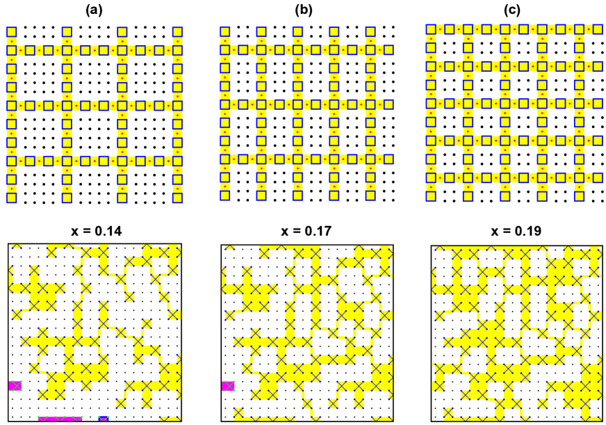
Figure 21: “Crowded” crossed wires that have high and . The crossed metallic wires are one plaquette in width. The symbols in the metallic wires are defined in Figures 18 and 19, with one change solely for clarity. Here, the added dopant (solid red square) that overlaps two plaquettes (blue squares) does not have a red square boundary. The black circles are undoped AF Cu spins. The first row of (a), (b), and (c) show crossed wires with , , and AF spins, respectively, inside each interior region formed by the perpendicular wires on CuO2 lattices. The second row shows the corresponding lattices that are randomly doped to approximately the same fraction of metallic unit cells as the crossed wires in the first row (, and ). Larger lattice figures for the second row can be found in Figures S14, S17, and S19 at the end of the paper. The for each wire configuration is approximately equal to the S-wave for an optimally doped system since the ratio of the surface metal cells to the total metal cells is 68%, 75%, and 80% for (a), (b), and (c), respectively. The ratio is at random optimal doping. The ’s of (a), (b), and (c) are approximately 12%, 8%, and 6% less than the S-wave at optimal doping. The for (a) is , where is the theoretical maximum of for YBa2Cu3O7-δ. In (b), and for currents along the x and y-axes, respectively. For (c), . Random optimal doping leads to (see Figure 4). Crossed metallic wires with varying aspect ratios and widths provide many opportunities for optimizing and for specific applications. For example, wires that are four metallic atoms wide (equal to two adjacent plaquettes in cuprates), would have the surface to total metal ratio of metallic wires two atoms wide (or one plaquette in cuprates), leading to an reduction in compared to wires that are two metallic atoms wide. However, increases by a factor of two.
Generally, it is most favorable to fabricate the narrowest wires that are spaced closely together because both and will be large. In addition, interfacial phonon modes will couple to both the closest wire and the next-nearest neighboring wire, leading to further increase in .
For cuprates, the narrowest wire is one plaquette width (see Figure 2). Other materials will have a different minimum width scale for wires.
-
•
Atomic-Scale metal-insulator inhomogeneity in a 3D material leads to a high- 3D S-wave pairing wavefunction. A 3D material is more stable against defects and grain boundaries.
-
•
Metallic and insulating regions provide new opportunities for pinning magnetic flux.
Strong pinning of magnetic flux lines in superconductors is necessary to obtain large critical current densities, . Insulating “pockets” surrounded by metallic region are energetically favorable for magnetic flux to penetrate. The flux can be strongly bound inside these insulating regions by adding further pinning centers to the insulating region. Examples of insulating pockets are shown in Figure 21.
-
•
In cuprates, freeze the fluctuating dumbbells in non-overlapping plaquettes while maintaining a metallic footprint with a large surface metallic unit cells to total metallic unit cells ratio.
The ratio of the isotropic S-wave pairing wavefunction to the corresponding D-wave is (see Figure 19).
-
•
In cuprates, fluctuating dumbbells in non-overlapping plaquettes can be frozen by breaking the symmetry inside each plaquette by an atomic substitution into the CuO2 plane, atomic substitution out of the CuO2 plane (such as the apical O atom sites), or interstitial atoms, as shown in Figure 22.
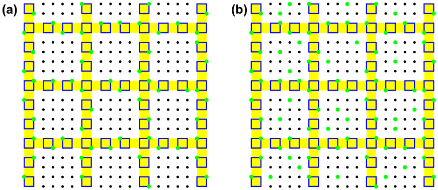
Figure 22: Atomic substitution inside non-overlapping plaquettes can freeze dumbbells by breaking the dumbbell degeneracy inside the plaquette. (a) and (b) show CuO2 lattices with AF interiors and crossing metallic wires one plaquette in width. In (a), the green dots show random atomic substitutions or interstitial atoms inside the plaquettes. The atomic substitutions may occur at the Cu atom in the plaquette (shown here), the O atoms inside the CuO2 plaquette, or the apical O atom sites. The O atoms are not shown in the figure. (b), green dots representing atomic substitutions or interstitial atoms in the insulating AF region are also shown. So long as these green dots do not disrupt the insulating behavior of these regions, the superconductivity will not be disturbed. (b) may be easier to engineer than (a) because the green dots are dispersed more randomly.
Conclusions
We have constructed a microscopic theory of cuprate superconductivity from the results of the chemist’s ab initio hybrid density functional methods (DFT). Hybrid DFT finds a localized out-of-the-CuO2 hole is formed around a negatively charged dopant. The doped hole resides in a four-Cu-site plaquette. The out-of-plane hole destroys the antiferromagnetism inside the plaquette and creates a tiny piece of metal there. Hence, the crystal is inhomogeneous on the atomic-scale with metallic and insulating regions.
In contrast, the physicist’s DFT methods (LDA and PBE) find a delocalized hole residing in the CuO2 planes as a consequence of doping. We argue that the chemist’s result is to be trusted over the physicist’s result because it corrects the spurious self-Coulomb repulsion of the electrons found in the physicist’s density functionals.
Due to dopant-dopant Coulomb repulsion, doped plaquettes do not overlap unless the doping is sufficiently high that overlap cannot be avoided. Non-overlapping plaquettes have a dynamic Jahn-Teller distortion of the out-of-the-plane hole that we call a “fluctuating dumbbell”. The dumbbells inside an overlapped plaquette become static Jahn-Teller distortions, or “frozen”.
The above model explains a vast swath of normal state phenomenolgy using simple counting of the sizes of the metallic region, the insulating AF region, and the number of flutuating and frozen dumbbells. We show that superconducting pairing arises from planar Oxygen atoms near the interface between the metallic and insulating regions. These planar O atom phonon modes explain the large K, the -dome as a function of doping, the changes in as a function of the number of CuO2 layers per unit cell, the lack of a isotope effect at optimal doping, and the D-wave superconducting pairing wavefunction (or superconducting gap symmetry).
Generally, with phonon superconducting pairing, an isotropic S-wave pairing wavefunction is favored over a D-wave pairing wavefunction. However, we show that the fluctuating dumbbells drastically raise the Cooper pair Coulomb repulsion, leading to the observed D-wave pairing wavefunction. By overlapping the plaquettes and freezing the dumbbells, the S-wave pairing wavefunction becomes favored over the D-wave pairing wavefunction. We show that the S-wave is in the range of K when the D-wave K.
Finally, we summarize the materials charateristics that are relevant for fabricating room-temperature superconductors and high current densities.
Acknowledgments
“In Ogg’s theory it was his intent
That the current keep flowing, once sent;
So to save himself trouble,
He put them in double,
And instead of stopping, it went.”
George GamovBlatt-book
The author thanks Professor Philip B. Allen for a discussion on estimating the electron-phonon coupling magnitude. The author is grateful to Professors William A. Goddard III and Carver A. Mead for discussions and encouragement.
References
- (1) Schilling, A., Cantoni, M., Guo, J. D. & Ott, H. R. Superconductivity Above 130 K in the Hg-Ba-Ca-Cu-O System. Nature 363, 56–58 (1993). URL http://dx.doi.org/10.1038/363056a0.
- (2) Mukuda, H., Shimizu, S., Iyo, A. & Kitaoka, Y. High-tc superconductivity and antiferromagnetism in multilayered copper oxides–a new paradigm of superconducting mechanism. Journal of the Physical Society of Japan 81, 011008 (2012). URL http://dx.doi.org/10.1143/JPSJ.81.011008.
- (3) Mann, A. Still in suspense. Nature 475, 280–282 (2011). URL http://dx.doi.org/10.1038/475280a.
- (4) Perdew, J. P., Burke, K. & Ernzerhof, M. Generalized gradient approximation made simple. Phys. Rev. Lett. 77, 3865–3868 (1996). URL http://link.aps.org/doi/10.1103/PhysRevLett.77.3865.
- (5) Yu, J. J., Freeman, A. J. & Xu, J. H. Electronically driven instabilities and superconductivity in the layered la2-xbaxcuo4 perovskites. Physical Review Letters 58, 1035–1037 (1987). URL http://link.aps.org/doi/10.1103/PhysRevLett.58.1035.
- (6) Mattheiss, L. F. Electronic band properties and superconductivity in la2-yxycuo4. Physical Review Letters 58, 1028–1030 (1987). URL http://link.aps.org/doi/10.1103/PhysRevLett.58.1028.
- (7) Pickett, W. E. Electronic-structure of the high-temperature oxide superconductors. Reviews of Modern Physics 61, 433–512 (1989). URL http://link.aps.org/doi/10.1103/RevModPhys.61.433.
- (8) Perdew, J. P. & Zunger, A. Self-interaction correction to density-functional approximations for many-electron systems. Phys. Rev. B 23, 5048–5079 (1981). URL http://link.aps.org/doi/10.1103/PhysRevB.23.5048.
- (9) Perry, J. K., Tahir-Kheli, J. & Goddard, W. A. Antiferromagnetic band structure of la2cuo4: Becke-3-lee-yang-parr calculations. Physical Review B 63, 144510 (2001). URL http://link.aps.org/doi/10.1103/PhysRevB.63.144510.
- (10) Perry, J. K., Tahir-Kheli, J. & Goddard, W. A. Ab initio evidence for the formation of impurity d3z2-r2 holes in doped la2-xsrxcuo4. Physical Review B 65, 144501 (2002). URL http://link.aps.org/doi/10.1103/PhysRevB.65.144501.
- (11) Tahir-Kheli, J. & Goddard, W. A. Origin of the pseudogap in high-temperature cuprate superconductors. Journal of Physical Chemistry Letters 2, 2326–2330 (2011). URL http://dx.doi.org/10.1021/jz200916t.
- (12) Tahir-Kheli, J. Understanding superconductivity in cuprates. Caltech YouTube Channel (2015). URL https://www.youtube.com/watch?v=Dq2uIzS_U9k.
- (13) Tahir-Kheli, J. Resistance of high-temperature cuprate superconductors. New Journal of Physics 15, 073020 (2013). URL http://stacks.iop.org/1367-2630/15/i=7/a=073020.
- (14) Tahir-Kheli, J. & Goddard, W. A. Universal properties of cuprate superconductors: Tc phase diagram, room-temperature thermopower, neutron spin resonance, and stm incommensurability explained in terms of chiral plaquette pairing. Journal of Physical Chemistry Letters 1, 1290–1295 (2010). URL http://dx.doi.org/10.1021/jz100265k.
- (15) Proust, C., Vignolle, B., Levallois, J., Adachi, S. & Hussey, N. E. Fermi liquid behavior of the in-plane resistivity in the pseudogap state of yba2cu4o8. Proceedings of the National Academy of Sciences 113, 13654–13659 (2016). URL http://www.pnas.org/content/113/48/13654.abstract.
- (16) Allen, P. B. & Mitrovic, B. Theory of superconducting . In Ehrenreich, H., Seitz, F. & Turnbull, D. (eds.) Solid State Physics, Advances in Research and Applications, vol. 37, 1–92 (Academic Press, New York, 1982).
- (17) Hashimoto, M. et al. Doping evolution of the electronic structure in the single-layer cuprate : Comparison with other single-layer cuprates. Phys. Rev. B 77, 094516 (2008). URL http://link.aps.org/doi/10.1103/PhysRevB.77.094516.
- (18) Pintschovius, L. Electron-phonon coupling effects explored by inelastic neutron scattering. Physica Status Solidi B-Basic Research 242, 30–50 (2005). URL http://dx.doi.org/10.1002/pssb.200404951.
- (19) Phillips, J. C. Self-organized networks and lattice effects in high-temperature superconductors. Phys. Rev. B 75, 214503 (2007). URL http://link.aps.org/doi/10.1103/PhysRevB.75.214503.
- (20) Li, C. W. et al. Structural relationship between negative thermal expansion and quartic anharmonicity of cubic . Phys. Rev. Lett. 107, 195504 (2011). URL http://link.aps.org/doi/10.1103/PhysRevLett.107.195504.
- (21) Lan, T. et al. Anharmonic lattice dynamics of studied by inelastic neutron scattering and first-principles molecular dynamics simulations. Phys. Rev. B 89, 054306 (2014). URL http://link.aps.org/doi/10.1103/PhysRevB.89.054306.
- (22) Hui, J. C. K. & Allen, P. B. Effect of lattice anharmonicity on superconductivity. Journal of Physics F: Metal Physics 4, L42 (1974). URL http://stacks.iop.org/0305-4608/4/i=3/a=003.
- (23) Crespi, V. H., Cohen, M. L. & Penn, D. R. Anharmonic phonons and the isotope effect in superconductivity. Phys. Rev. B 43, 12921–12924 (1991). URL http://link.aps.org/doi/10.1103/PhysRevB.43.12921.
- (24) Crespi, V. H. & Cohen, M. L. Anharmonic phonons and the anomalous isotope effect in . Phys. Rev. B 44, 4712–4715 (1991). URL http://link.aps.org/doi/10.1103/PhysRevB.44.4712.
- (25) Crespi, V. H. & Cohen, M. L. Anharmonic phonons and high-temperature superconductivity. Phys. Rev. B 48, 398–406 (1993). URL http://link.aps.org/doi/10.1103/PhysRevB.48.398.
- (26) Keller, H. Unconventional isotope effects in cuprate superconductors. In Müller, K. A. & Bussmann-Holder, A. (eds.) In Superconductivity in Complex Systems. Springer Series Structure and Bonding, vol. 114, 143–169 (Springer Berlin Heidelberg, Berlin, Heidelberg, 2005). URL http://dx.doi.org/10.1007/b101019.
- (27) Keller, H., Bussmann-Holder, A. & Müller, K. A. Jahn–teller physics and high-tc superconductivity. Materials Today 11, 38 – 46 (2008). URL http://www.sciencedirect.com/science/article/pii/S1369702108701780.
- (28) de Gennes, P. G. Superconductivity of Metals and Alloys (Addison-Wesley Publishing Co., Inc., Redwood City, California, 1989).
- (29) Schreiffer, J. R. Theory of Superconductivity (Perseus Books, Reading, Massachusetts, 1999).
- (30) Bogoliubov, N. N., Tolmachev, V. V. & Shirkov, D. V. A New Method in the Theory of Superconductivity (Consultants Bureau, Inc., New York, 1959).
- (31) Morel, P. & Anderson, P. W. Calculation of the superconducting state parameters with retarded electron-phonon interaction. Phys. Rev. 125, 1263–1271 (1962). URL http://link.aps.org/doi/10.1103/PhysRev.125.1263.
- (32) Cohen, M. L. Superconductivity in low-carrier density systems: Degenerate semiconductors. In Parks, R. D. (ed.) Superconductivity, vol. 1, 615–664 (Marcel Dekker, Inc., New York, 1969).
- (33) Tsuei, C. C. & Kirtley, J. R. Pairing symmetry in cuprate superconductors. Rev. Mod. Phys. 72, 969–1016 (2000). URL http://link.aps.org/doi/10.1103/RevModPhys.72.969.
- (34) Schrieffer, J. R., Scalapino, D. J. & Wilkins, J. W. Effective tunneling density of states in superconductors. Phys. Rev. Lett. 10, 336–339 (1963). URL http://link.aps.org/doi/10.1103/PhysRevLett.10.336.
- (35) Scalapino, D. J., Schrieffer, J. R. & Wilkins, J. W. Strong-coupling superconductivity. i. Phys. Rev. 148, 263–279 (1966). URL http://link.aps.org/doi/10.1103/PhysRev.148.263.
- (36) Karppinen, M. et al. Layer-specific hole concentrations in bi2sr2y1-xcaxcu2o8+δ as probed by xanes spectroscopy and coulometric redox analysis. Phys. Rev. B 67, 134522 (2003). URL http://link.aps.org/doi/10.1103/PhysRevB.67.134522.
- (37) Liang, R., Bonn, D. A. & Hardy, W. N. Evaluation of plane hole doping in single crystals. Phys. Rev. B 73, 180505 (2006). URL http://link.aps.org/doi/10.1103/PhysRevB.73.180505.
- (38) Naqib, S. H., Cooper, J. R., Tallon, J. L. & Panagopoulos, C. Temperature dependence of electrical resistivity of high-t-c cuprates - from pseudogap to overdoped regions. Physica C-Superconductivity and Its Applications 387, 365–372 (2003). URL http://dx.doi.org/10.1016/S0921-4534(02)02330-4.
- (39) Yoshida, T. et al. Low-energy electronic structure of the high-tc cuprates la2-xsrxcuo4 studied by angle-resolved photoemission spectroscopy. Journal of Physics: Condensed Matter 19, 125209 (2007). URL http://stacks.iop.org/0953-8984/19/i=12/a=125209.
- (40) Ono, S. & Ando, Y. Evolution of the resistivity anisotropy in bi2sr2-xlaxcuo6+δ single crystals for a wide range of hole doping. Phys. Rev. B 67, 104512 (2003). URL http://link.aps.org/doi/10.1103/PhysRevB.67.104512.
- (41) Bangura, A. F. et al. Fermi surface and electronic homogeneity of the overdoped cuprate superconductor tl2ba2cuo6+δ as revealed by quantum oscillations. Phys. Rev. B 82, 140501 (2010). URL http://link.aps.org/doi/10.1103/PhysRevB.82.140501.
- (42) Rourke, P. M. C. et al. A detailed de haas–van alphen effect study of the overdoped cuprate tl2ba2cuo6+δ. New Journal of Physics 12, 105009 (2010). URL http://stacks.iop.org/1367-2630/12/i=10/a=105009.
- (43) Kurtin, S., McGill, T. C. & Mead, C. A. Fundamental transition in the electronic nature of solids. Phys. Rev. Lett. 22, 1433–1436 (1969). URL http://link.aps.org/doi/10.1103/PhysRevLett.22.1433.
- (44) Takagi, H. et al. Superconductor-to-nonsuperconductor transition in as investigated by transport and magnetic measurements. Phys. Rev. B 40, 2254–2261 (1989). URL http://link.aps.org/doi/10.1103/PhysRevB.40.2254.
- (45) Herzberg, G. Molecular Spectra and Molecular Structure I. Spectra of Diatomic Molecules (D. Van Nostrand Company, Inc. Princeton, New Jersey, 1950).
- (46) Herzberg, G. Molecular Spectra and Molecular Structure II. Infrared and Raman Spectra of Polyatomic Molecules (D. Van Nostrand Company, Inc. Princeton, New Jersey, 1945).
- (47) Wilson, E. B., Decius, J. C. & Cross, P. C. Molecular Vibrations. The Theory of Infrared and Raman Vibrational Spectra (Dover Publications, Inc., New York, 1980).
- (48) Pereiro, J. et al. Insights from the study of high-temperature interface superconductivity. Philosophical Transactions of the Royal Society of London A: Mathematical, Physical and Engineering Sciences 370, 4890–4903 (2012). URL http://rsta.royalsocietypublishing.org/content/370/1977/4890.
- (49) Allen, P. B. & Dynes, R. C. Transition temperature of strong-coupled superconductors reanalyzed. Phys. Rev. B 12, 905–922 (1975). URL http://link.aps.org/doi/10.1103/PhysRevB.12.905.
- (50) Blatt, J. M. Theory of Superconductivity (Academic Press Inc., New York and London, 1964).
- (51) Ginder, J. M. et al. Photoexcitations in : 2-ev energy gap and long-lived defect states. Phys. Rev. B 37, 7506–7509 (1988). URL http://link.aps.org/doi/10.1103/PhysRevB.37.7506.
- (52) Zhang, F. C. & Rice, T. M. Effective hamiltonian for the superconducting cu oxides. Phys. Rev. B 37, 3759–3761 (1988). URL http://link.aps.org/doi/10.1103/PhysRevB.37.3759.
- (53) Becke, A. D. Density-functional thermochemistry. iii. the role of exact exchange. J. Chem. Phys. 98, 5648–5652 (1993). URL http://scitation.aip.org/content/aip/journal/jcp/98/7/10.1063%/1.464913.
- (54) Crowley, J. M., Tahir-Kheli, J. & Goddard, W. A. Resolution of the band gap prediction problem for materials design. J. Phys. Chem. Lett. 7, 1198–1203 (2016). URL http://dx.doi.org/10.1021/acs.jpclett.5b02870.
- (55) Saunders, V. et al. CRYSTAL98 User’s Manual (University of Torino: Torino, 1998).
- (56) Lee, C., Yang, W. & Parr, R. G. Development of the colle-salvetti correlation-energy formula into a functional of the electron density. Phys. Rev. B 37, 785–789 (1988). URL http://link.aps.org/doi/10.1103/PhysRevB.37.785.
- (57) CRYSTAL98 only had basic Fock Matrix mixing convergence (SCF) at the time of our calculation in 2001.Perry2001 Using the most recent version of CRYSTAL (2015), we find the gap to be 3.1 eV using exactly the same basis set. Improved SCF convergence algorithms, increased computing power, and memory indicates our result of 2001 had not fully converged. We know hybrid functionals generally overestimate the band gaps of Mott antiferromagnets by eV,Crowley2016 perhaps because the unrestricted spin wavefunctions (UHF) do not represent the correct spin state. Regardless, the orbital character of the doped hole is unchanged. None of the conclusions of the current paper are altered.
- (58) Hybertsen, M. S., Stechel, E. B., Foulkes, W. M. C. & Schluter, M. Model for low-energy electronic states probed by x-ray absorption in high-tc cuprates. Physical Review B 45, 10032–10050 (1992). URL http://link.aps.org/doi/10.1103/PhysRevB.45.10032.
- (59) Scalapino, D. J. The electron-phonon interaction and strong-coupling superconductors. In Parks, R. D. (ed.) Superconductivity, vol. 1, 449–560 (Marcel Dekker, Inc., New York, 1969).
- (60) Vidberg, H. J. & Serene, J. W. Solving the eliashberg equations by means of n-point padé approximants. Journal of Low Temperature Physics 29, 179–192 (1977). URL http://dx.doi.org/10.1007/BF00655090.
- (61) Leavens, C. & Ritchie, D. Extension of the n-point padé approximants solution of the eliashberg equations to t tc. Solid State Communications 53, 137 – 142 (1985). URL http://www.sciencedirect.com/science/article/pii/003810988590%1127.
- (62) Beach, K. S. D., Gooding, R. J. & Marsiglio, F. Reliable padé analytical continuation method based on a high-accuracy symbolic computation algorithm. Phys. Rev. B 61, 5147–5157 (2000). URL http://link.aps.org/doi/10.1103/PhysRevB.61.5147.
- (63) Östlin, A., Chioncel, L. & Vitos, L. One-particle spectral function and analytic continuation for many-body implementation in the exact muffin-tin orbitals method. Phys. Rev. B 86, 235107 (2012). URL http://link.aps.org/doi/10.1103/PhysRevB.86.235107.
- (64) Elliott, R. J., Krumhansl, J. A. & Leath, P. L. The theory and properties of randomly disordered crystals and related physical systems. Rev. Mod. Phys. 46, 465–543 (1974). URL http://link.aps.org/doi/10.1103/RevModPhys.46.465.
- (65) Hussey, N. E. et al. Dichotomy in the t-linear resistivity in hole-doped cuprates. Philosophical Transactions of the Royal Society a-Mathematical Physical and Engineering Sciences 369, 1626–1639 (2011). URL http://rsta.royalsocietypublishing.org/content/369/1941/1626.
- (66) Abdel-Jawad, M. et al. Anisotropic scattering and anomalous normal-state transport in a high-temperature superconductor. Nature Physics 2, 821–825 (2006). URL http://dx.doi.org/10.1038/Nphys449.
- (67) Cooper, R. A. et al. Anomalous criticality in the electrical resistivity of la2-xsrxcuo4. Science 323, 603–607 (2009). URL http://dx.doi.org/10.1126/science.1165015.
Appendix A Analysis of Physicist and Chemist DFT
Since our prior normal state and current results depend on the assumption that the chemist’s out-of-the-CuO2 hole is correct, we discuss the physicist’s and chemist’s DFT approaches here.
Immediately following the discovery of cuprates in 1986, density functional (DFT) band structure calculations were performed using the local density approximation (LDA).Yu1987 ; Mattheiss1987 ; Pickett1989 These calculations all found the ground state of the undoped cuprates to be metallic rather than an insulating spin-1/2 antiferromagnet (AF) with a nonzero band gap of eV.Ginder1988 The orbital character of the electrons near the Fermi level was a mixture of planar Cu and planar O , where the x and y-axes and the orbitals point along the planar CuO bonds. Hence, LDA found the correct orbital character at the Fermi level. The problem was the electrons were not localized.
The reason for this error of LDA and the more modern PBE (Perdew-Burke-Ernzerhof) density functionalPBE arises because both LDA and PBE contain unphysical Coulomb repulsion of an electron with itselfPerdew1981 (known as the self-Coulomb repulsion). The self-repulsion spreads the electron density out, leading to greater electron hopping, and hence an increase of the valence and conduction band widths. The increased band widths reduce the gap. In the case of cuprates, the gap is reduced to zero.
Given the failure of state-of-the-art ab initio methods for the undoped AF insulator, two different approaches were taken. In the first approach, the hole created by a dopant was assumed to “knock out” one of the localized magnetic electrons by forming a spin singlet state (no magnetism) with the localized planar Cu spin and the neighboring planar O atoms orbitals to form a Zhang-Rice singlet.Zhang1988 This unmagnetized “hole” in the AF spin background could hop from planar Cu site to planar Cu site. The interaction of these holes with each other and with the AF background spins comprise the and classes of Hubbard models for cuprates.
The second approach argued that the metallic band structure found by ab initio computations was a reasonable starting point for understanding cuprates because, in the superconducting range of dopings, the high temperature phase is metallic. Hence, only the Fermi level needed to be lowered to the match the doping.
Both attacks assumed the only relevant orbitals for understanding cuprates are planar Cu and planar O . These two pictures dominate the 30 year literature on cuprates.
Chemically, neither of these two approaches makes sense. An out-of-plane hole dopant has a net negative charge relative to the undoped background. In analogy to acceptor (p-type) dopants in semiconductors, a localized level surrounding the dopant should be pulled out of the valence band (the acceptor level). For cuprates, the hole orbital should be localized and comprised of out-of-plane character pointing toward the dopant. Instead, ab-initio DFT and the above two approaches remove a delocalized electron with orbital character pointing away from the dopant (inside the CuO2 plane). If the acceptor impurity level was shallow (energy close to the top of the valence band), then at moderate temperatures, the hole will be in the valence band. In this case, the physicist’s hole state would be correct, except at the lowest temperatures. However, using the chemist’s DFT methods described below, the impurity state is found to be eV above the top of the valence band for a hole doping of () in La2-xSrxCuO4 (see Figure 4b of Perry et al.Perry2002 ). The acceptor level is a deep trap.
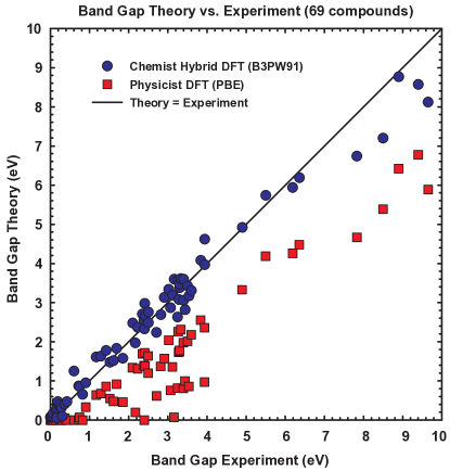
Obtaining the correct doped electronic structure for cuprates requires correcting the self-Coulomb repulsion error in the LDA and PBE functionals that led to an undoped metallic ground state. A correction appeared in 1993 (seven years after the discovery of cuprates) by BeckeB3PW with the invention of hybrid density functionals. Hybrid density functionals reduce the self-Coulomb repulsion by including exact Hartree-Fock exchange. In molecular chemistry, hybrid density functionals are superior to LDA and PBE, and have been the workhorses for ab initio computations over the past two decades. For crystalline materials, we have recently shownCrowley2016 that hybrid DFT functionals practically resolve the band gap prediction problem across the whole periodic table with a mean absolute deviation of eV, while PBE has an absolute error of eV. The LDA functional is worse than PBE and no numbers were reported.Crowley2016 These results are plotted in Figure 23.
Unfortunately, the appearance of the superior hybrid DFT method had no influence on the cuprate field. One possible explanation is that the ab initio band structure codes familiar to most physicists construct the Hamiltonian in a plane-wave basis set and the Hartree-Fock exchange term in hybrid DFT is computationally impractical in this basis space. Hybrid DFT becomes computationally practical using localized Gaussian basis sets. Localized basis sets are superior to plane-wave basis set for molecular problems and have been used extensively by ab initio quantum chemists. The first software to successfully implement hybrid DFT for solids was CRYSTAL98,CRYSTAL98 which used localized Gaussian basis functions. Regrettably, CRYSTAL98 appeared 12 years after the discovery of cuprate superconductivity.
Another possibility is historical. The solid state community has had enormous success for over 80 years assuming any inhomogeneity (such as impurities) is a small perturbation to a zeroth order Hamiltonian with full translational symmetry. Atomic-scale inhomogeneity of the kind suggested by the chemist’s DFT requires breaking translational symmetry at zeroth order.
Using the hybrid DFT functional, B3LYP (Becke-3-Lee-Yang-Parr),B3PW ; LYP we showedPerry2001 that a 2 eV band gap AF insulator is obtained 111 CRYSTAL98 only had basic Fock Matrix mixing convergence (SCF) at the time of our calculation in 2001.Perry2001 Using the most recent version of CRYSTAL (2015), we find the gap to be 3.1 eV using exactly the same basis set. Improved SCF convergence algorithms, increased computing power, and memory indicates our result of 2001 had not fully converged. We know hybrid functionals generally overestimate the band gaps of Mott antiferromagnets by eV,Crowley2016 perhaps because the unrestricted spin wavefunctions (UHF) do not represent the correct spin state. Regardless, the orbital character of the doped hole is unchanged. None of the conclusions of the current paper are altered. for undoped La2CuO4, in agreement with experiment.Ginder1988 Explicitly doped La2-xSrxCuO4 has hole states pointing out of the CuO2 plane towards the dopants.Perry2002 Thus, in the case of cuprates, hybrid DFT has led to a completely different electronic structure than the LDA or PBE hole, as shown in Figure 1. The success of hybrid DFT in molecular chemistry and for the band gaps in Figure 23 strongly suggests hybrid DFT should be trusted over LDA and PBE DFT results. We believe this mistake with the doped electronic structure led the entire field astray.
“If a mason building a wall puts the first stone in crooked,
no matter how tall the wall becomes, it will still be crooked.”
Saadi Shirazi, (Born , Died )
Appendix B Degeneracy at the Fermi Level in an Isolated Plaquette that Splits in the Crystal Environment and Leads to the Pseudogap
Appendix C Dumbbell Character of the Doped Plaquette Hole
Appendix D Estimate of the Magnitude of the Electron-Phonon Coupling, g
It is known to be qualitatively correct that where is the Debye energy, is the Fermi energy, is the electron mass, and is the nuclear mass. One can quickly see that the form of the above expression is correct using where is the spring constant and due to metallic electron screening.
The electron-phonon coupling, , is of the form , where is the nuclear potential energy. Substituting , leads to . Hence, .
Another derivation is dimensional. The coupling, , has dimensions of energy and there are only two relevant energy scales, and . Thus there are three possibilities for : the mean, the geometric mean, and the harmonic mean of and . Since , the mean is , and the harmonic mean is . Neither of these two means makes intuitive sense because we know metallic electrons strongly screen the nuclear-nuclear potential. The only sensible choice is the geometric mean, .
Appendix E Fluctuation Tc: Plaquette Clusters Smaller than the Coherence Length
There are superconducting fluctuations above at low dopings due to the fluctuating magenta plaquette clusters in Figures 8, 9, and 10. These plaquette clusters have superconducting pairing that does not contribute to the observed because the clusters are smaller than the coherence length. Including these clusters into the computation leads to an estimate of the temperature range where plaquette cluster superconducting fluctuations occur above . The resulting “fluctuation domes” are plotted in Figure 26. Of course, there exist superconducting fluctuations above from the plaquettes clusters that are larger than the coherence length (yellow clusters in Figures 8, 9, and 10). The fluctuation from the larger yellow clusters is not included in figure 26.
Appendix F Parameters Used in the Tc Computations
| (eV) | (eV) | (eV) | |
|---|---|---|---|
| 0.84 | 0.25 | -0.05625 | 0.08 |
| (dimensionless) | (Kelvin) | (Kelvin) | (eV) | (eV) |
|---|---|---|---|---|
| 0.5 | 300 | 1.0 | 0.3 | 0.06 |
| Next Layer | ||||||||||
|---|---|---|---|---|---|---|---|---|---|---|
| Figure | Curve Color | Edge | Convex | Concave | Edge | Convex | Concave | |||
| 16 | Black | 20 | 0.150 | 0.150 | 0.075 | 0.240 | 0.240 | 0.120 | ||
| 16 | Magenta | 20 | 0.150 | 0.150 | 0.075 | 0.130 | 0.130 | 0.065 | ||
| 16 | Red | 100 | 0.000 | 0.000 | 0.000 | 0.132 | 0.132 | 0.000 | ||
| 26 | Blue | 8 | 0.150 | 0.150 | 0.075 | 0.240 | 0.240 | 0.120 | ||
| 26 | Green | 12 | 0.150 | 0.150 | 0.075 | 0.240 | 0.240 | 0.120 | ||
| 26 | Red | 16 | 0.150 | 0.150 | 0.075 | 0.240 | 0.240 | 0.120 | ||
| 26 | Black | 20 | 0.150 | 0.150 | 0.075 | 0.240 | 0.240 | 0.120 | ||
| 17 | Black | 20 | 0.150 | 0.150 | 0.075 | 0.240 | 0.240 | 0.120 | 0.0 | 0.2 |
| 17 | Blue | 20 | 0.050 | 0.000 | 0.000 | 0.130 | 0.130 | 0.065 | 0.05 | 0.13 |
| Layers | Hole Doping per CuO2 Layer | |||||||||
|---|---|---|---|---|---|---|---|---|---|---|
| 1 | 0.16 | |||||||||
| 2 | 0.16 | 0.16 | ||||||||
| 3 | 0.16 | 0.11 | 0.16 | |||||||
| 4 | 0.16 | 0.11 | 0.11 | 0.16 | ||||||
| 5 | 0.16 | 0.11 | 0.09 | 0.11 | 0.16 | |||||
| 6 | 0.16 | 0.11 | 0.09 | 0.09 | 0.11 | 0.16 | ||||
| 7 | 0.16 | 0.11 | 0.09 | 0.09 | 0.09 | 0.11 | 0.16 | |||
| 8 | 0.16 | 0.11 | 0.09 | 0.09 | 0.09 | 0.09 | 0.11 | 0.16 | ||
| 9 | 0.16 | 0.11 | 0.09 | 0.09 | 0.09 | 0.09 | 0.09 | 0.11 | 0.16 | |
| 10 | 0.16 | 0.11 | 0.09 | 0.09 | 0.09 | 0.09 | 0.09 | 0.09 | 0.11 | 0.16 |
Appendix G Description of the Eliashberg Calculations
G.1 The Eliashberg Equations
The attractive electron-electron pairing mediated by phonons is not instantaneous in time due to the non-zero frequency of the phonon modes (phonon retardation). In addition, electrons are scattered by phonons leading to electron wavefunction renormalization (“lifetime effects”) that decrease . Any credible prediction must incorporate both of these effects. All calculations in this paper solve the Eliashberg equations for the superconducting pairing wavefunction (also called the gap function). It includes both the pairing retardation and the electron lifetime.Schrieffer-book ; Allen1982 ; Scalapino1969
The Eliashberg equations are non-linear equations for the superconducting gap function, , and the wave function renormalization, , as a function of momentum , frequency , and temperature . Usually, the dependence of and is assumed, and they are written as and , respectively. We follow this convention here. Both and are a complex numbers. In this Appendix only, we will absorb Boltzmann’s constant, , into . Thus has units of energy.
Both and are frequency dependent because of the non-instantaneous nature of the superconducting electron-electron pairing. If the pairing via phonons was instantaneous in time, then there would be no frequency dependence to and . The simpler BCSSchrieffer-book gap equation assumes an instantaneous pairing interaction ( is independent of ) and no wavefunction renormalization ().
The Eliashberg equations may be solved in momentum and frequency space , or in momentum and discrete imaginary frequency space, , where is an integer and . In the imaginary frequency space representation, the temperature dependence and the retardation of the phonon induced pairing are both absorbed into the imaginary frequency dependence, . In theory, both and can be obtained by analytic continuation of their counterparts. In practice, the analytic continuation is fraught with numerical difficulties.Vidberg1977 ; Leavens1985 ; Beach2000 ; Ostlin2012 However, the symmetry of the gap can be extracted from either the real or imaginary frequency representations of .
In the pioneering work of Schrieffer, Scalapino, and Wilkins,Schrieffer1963 ; Scalapino1966 ; Schrieffer-book ; Scalapino1969 the goal was to obtain the isotropic (in -space) gap function at zero temperature, , as a function of in order to compute the superconducting tunneling of lead ( K). Hence, they solved the full non-linear Eliashberg equations in frequency space.
Above , is zero. For , is small. Since our interest in this paper is on the magnitude of and the symmetry of the superconducting gap, we can linearize the gap, , in the Eliashberg equations for temperatures, , close to . The result is a temperature dependent real symmetric matrix eigenvalue equation with as the eigenvector. The eigenvalues are dimensionless and the largest eigenvalue monotonically increases as decreases. For , the largest eigenvalue of the real symmetric matrix is less than 1. At , the largest eigenvalue equals 1, signifying the onset of superconductivity.
The non-linear Eliashberg equations (or the linearized version) are easier to solve in imaginary frequency space.Allen1982 Hence, we solve the linearized Eliashberg equations in imaginary frequency space to obtain .
We use the linearized Eliashberg equations as derived in the excellent chapter by Allen and Mitrovic.Allen1982 Prior Eliashberg formulations assume translational symmetry (momentum is a good quantum number for the metallic states). Our metallic wavefunctions are not states because they are only non-zero in the percolating metallic region. We write the wavefunction and energy for the state with index as and , respectively. Since is only delocalized over the metallic region and is normalized, , where is the total number of metallic Cu sites. Rather than Cooper pairing occuring between and its time-reversed partner, , a Cooper pair here is comprised of , where is the complex conjugate of .
The linearized Eliashberg equations for and are obtained from the -vector equationsAllen1982 simply by replacing with the index everywhere
| (1) | |||||
| (2) | |||||
where is the Fermi energy, is the total metallic density of states per spin per energy, is the sign of , is the cutoff energy for the frequency sums, is the dimensionless phonon pairing strength (defined below), and is the dimensionless Morel-Anderson Coulomb pseudopotential at cutoff energy . It is a real number. The wavefunction renormalization, , is dimensionless. In the non-linear Eliashberg equations, has units of energy. In the linearized equations above, is an eigenvector and is arbitrary up to a constant factor.
The “electron-phonon spectral function” is defined
| (3) |
and the phonon pairing strength is defined
| (4) | |||||
| (5) |
where is the matrix element (units of energy) between initial and final states and , respectively of the electron-phonon coupling, and is the electron-phonon coupling for the phonon mode with energy . Both and are real positive numbers. Hence, is a real positive number. From 2, the gap can always be chosen to be real. Since from equation 4,
| (6) | |||||
| (7) |
and are dimensionless because . Physically, they should be independent of the number of metallic Cu sites, , as becomes infinite. The independence with respect to is shown below.
The electron-phonon Hamiltonian for phonon mode , , is
| (8) |
where is the nuclear mass. and destroy and create phonon modes, respectively. is the potential energy of the electron. For localized phonon modes, is independent of the number of metallic sites, . The and metallic states each scale as , leading to . Since the number of localized phonon modes scales as , the scaling of the sum is . Hence, we have shown that and are dimensionless and independent of because the density of states per spin, , is proportional to . In fact, and are independent of even when the phonon modes are delocalized. In this case, . The electron-phonon matrix element is now summed over the crystal, and thereby picks up a factor of . Hence, . For delocalized phonons, the sum over phonon modes in does not add another factor of . The claim is obvious when and are momentum states and because the only phonon mode that connects these two states has momentum . Therefore, and are always dimensionless and independent of .
The atomic-scale inhomogeneity of cuprates implies translation is not a perfect symmetry of the crystal. However, the dopants are distributed randomly, and therefore on average becomes a good quantum number. Hence, we may work with Green’s functions in space and approximate the Cooper pairing to occur between states. The approximation is identical to the very successful Virtual Crystal Approximation (VCA) and the Coherent Potential Approximation (CPA) for random alloys.CPA
In the VCA and CPA, the Green’s function between two distinct states, and is zero
| (9) |
The fact that is not a good quantum number of the crystal is incorporated by including a self-energy correction, at zeroth order into the metallic Green’s function
| (10) |
Here, is the bare electron energy. can be written as the sum of two terms, . Both and are even powers of , , for . adds a shift to the bare electron energy, , and a lifetime broadening to the electronic state. leads to wavefunction renormalization of the bare electron state.
The shift of due to leads to the observed angle-resolved photoemission (ARPES) band structure in cuprates,Hashimoto2008 , and its lifetime broadening. The lifetime broadening integrates out of the Eliashberg equations because the integral of a Lorentzian across the Fermi energy is independent of the width of the Lorentzian.Allen1982 Hence, we may use the ARPES band structure, , in the Eliashberg equations and absorb into in the Eliashberg equations.
Hence, we are right back to the standard Eliashberg equationsAllen1982 ; Schrieffer-book ; Schrieffer1963 ; Scalapino1966 ; Scalapino1969
| (12) | |||||
| (13) |
The Eliashberg equations above are completely general for a single band crossing the Fermi level. The only inputs into the equations are the Fermi surface, Fermi velocity (in order to obtain the local density of states), the dimensionless electron-phonon pairing, , and the dimensionless Morel-Anderson Coulomb pseudopotential at the cutoff energy (typically, chosen to be five times larger than the highest phonon mode, ), . We apply the standard methodsAllen1982 to map the above equations into a matrix equation for the highest eigenvalue as a function of . The highest eigenvalue monotonically increases at decreases. When the highest eigenvalue crosses 1, is found.
Equations G.1, 12, 13 need to be modified when more than one band crosses the Fermi level. Phonons can scatter electron pairs from one band to another in addition to scattering within a single band. The modification to the single Fermi surface Eliashberg equations above require changing the and labels to and where and refer to the band index. and remain vectors in 2D so long as we assume the coupling of CuO2 layers in different unit cells is weak. The number of bands is equal to the number of CuO2 layers per unit cell, . We derive the electron-phonon pairing for a single layer cuprate in sections G.2 and G.3. In section G.4, we derive the multi-layer .
The total electron-phonon spectral function is the sum of four terms
| (14) |
where and are the spectral functions from phonons that contribute to the resistivity. is due to the phonons that lead to the low-temperature linear term in the resistivity, and is due to the phonons that lead to the the low-temperature resistivity term.Hussey2011 is the component due to the planar O atom at the surface between the metal and insulating regions. It is the O atom phonon shown in Figure 12a. is the contribution from the planar O atom adjacent to the metal-insulator surface on the insulating AF side. It is shown in Figure 12b. Since the energy of these two O phonons modes is meV,Pintschovius2005 their contribution to the resistivity is very small.
G.2 Contribution to from the Interface O Atom Phonons in Figure 12
G.2.1 Surface O Atom Mode in Figure 12a
The Hamiltonian for Figure 27 is
| (15) |
where and create and destroy an electron at the Cu site. and are defined similarly. Since there is no electron spin coupling to the O atom phonon mode, the electron spin index is dropped in equation 15.
The state is defined as
| (16) |
where is the localized effective Cu orbital at position , and is the number of metallic Cu sites. The matrix element between and is
| (17) |
The modulus squared is
| (18) | |||||
Define the two functions of and , and as
| (19) | |||||
| (20) | |||||
where is the average of the function defined for each planar surface O on the x-axis with position as shown in Figure 27,
| (21) |
Similary, is the average of over the y-axis surface O atoms. The expression in equation 20 for is identical to the expression for in equation 19 with replaced by .
| (22) |
G.2.2 O Atom Mode Perpendicular to Surface in Figure 12b
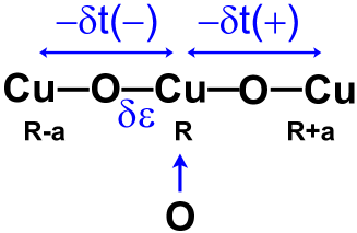
The Hamiltonian for Figure 28 is
| (23) |
where and create and destroy an electron at the Cu site. and are defined similarly. Since there is no electron spin coupling to the O atom phonon mode, the electron spin index is dropped in equation 23.
The matrix element between and is
| (24) |
The modulus squared is
| (25) | |||||
Define the two functions of and , and as
| (26) | |||||
| (27) | |||||
where is the average, defined in equation 21, of the function for each x-axis O phonon mode with position as shown in Figure 28. Similary, is the average of over the y-axis O atoms. The expression in equation 27 for is identical to the expression for in equation 26 with replaced by .
| (28) |
G.3 Contribution to from the Phonons Responsible for the the Resistivity
The low-temperature resistivity of La2-xSrxCuO4 is the sum of two terms.Hussey2011 One term is linear in and the other is proportional to . At high temperatures, both terms become linear in . Previously, we showedTahir-Kheli2013 that the doping evolution of these two terms can be explained by phonon scattering and simple counting of the number of metallic sites and the number of overlapped plaquettes, as a function of doping. The contribution of these phonons on must be included in our Eliashberg calculation.
The power law dependence of the two terms in the resistivity restricts the form of their electron-phonon spectral functions, and for the linear and contributions, respectively. From Fermi’s Golden Rule, the electron scattering rate is
| (29) |
where is the Bose-Einstein distribution . The factor of two in front of the integral comes from the absorption and emission of phonons. is zero for greater than the highest phonon energy.
At high temperatures, leading to , where
| (30) |
and . is called the mass-enhancement factor.Allen1982 The slope of the high-temperature scattering rate can be obtained from the resistivity. Hence, the mass-enhancement can be computed from experiment.
At low-temperatures, the Bose-Einstein distribution cuts the integral in the scattering rate off at . If , then
| (31) |
The low-temperature scattering rate is known to be isotropic in -space,Abdel-Jawad2006 and thereby it must scale as from equation 31. From the low-temperature resistivity experimentsHussey2011 , we showed the resistivity term was proportional to , where is the total number of Cu sites (metallic plus insulating AF sites) and is the number of metallic Cu sites that are in non-overlapping plaquettes. Therefore, is of the form
| (32) |
where is a constant to be determined. is the Debye energy. , for .
The low-temperature scattering rate is zero along the diagonals, , and large at .Abdel-Jawad2006 is independent of from equation 31. The scattering rate in equation 31 logarithmically diverges for small . Hence, it must be cutoff at some minimum, . For temperatures below , the scattering rate cannot be linear in . Previously, we showed that K.Tahir-Kheli2013 In this paper, we fix K. See Appendix F.
The spectral function, , is of the form
| (33) |
where is a constant, and outside of the range .
The anisotropy factor, , is
| (34) |
where the denominator is the average over the Fermi surface of the numerator.
The average of a function, , over the Fermi surface is defined as
| (35) |
Thus .
The constants and can be determined as follows. The average around the Fermi surface of the scattering rate at high-temperatures is . From resistivity measurements,Cooper2009 . A fraction of comes from and the fraction comes from leading to
| (36) |
| (37) |
Substituting and in terms of back into and yields
| (38) |
and
| (39) |
outside of the range and for .
We solve for , for using the -space version of equation 4
| (40) |
leading to
| (41) |
and
| (42) |
G.4 Generalization of the Eliashberg Equations for Multi-Layer Cuprates
The Eliashberg equations G.1, 12, and 13 for a single CuO2 layer per unit cell are generalized to multi-layer cuprates by changing and to and , respectively, in the single layer Eliashberg equations.
| (44) | |||||
| (45) |
where and are band indicies. They vary from to , where is the number of CuO2 layers per unit cell. A unit cell contains Cu atoms, one in each layer. The vector is a 2D vector. is the total density of states per spin
| (46) |
There is a Bloch state for each layer, , given by . The band eigenfunctions are
| (47) |
The coefficients, , are real since the inter-layer hopping matrix elements are real. The matrix element for hopping between adjacent layers is
| (48) |
where
| (49) |
The eigenvectors of equations 47 and 48 are independent of the magnitude of . Thus is independent of ,
| (50) |
The eigenstates, , are normalized leading to
| (51) |
| (52) |
The electron-phonon spectral function is
| (53) |
where
| (54) |
| (55) |
is the number of metallic Cu sites in layer that are in non-overlapping plaquettes, is the total number of CuO2 layers per unit cell, and is the total number of Cu sites (metallic plus insulating AF) in a single CuO2 layer. Hence, is the total number of Cu sites in the crystal and is the total fraction of metallic Cu sites over all the CuO2 layers. for .
For the electron-phonon spectral function, , that leads to the low-temperature linear resistivity, define the anisotropy factor, as
| (56) |
where the denominator is the average over all the Fermi surfaces of the numerator.
The average of a function, , over all the Fermi surfaces is defined as
| (57) |
The phonon modes in are 2D. Hence, the form of the spectral function between layers and is of the form,
| (58) |
Expanding the eigenstates in terms of from equation 47 leads to
| (59) |
where . , for or .
Hence,
| (60) |
and
| (61) |
The multi-layer expressions for and are similar to their single-layer counterparts with a modified definition for the averaging in their respective and functions.
| (62) | |||||
| (63) | |||||
where is the multi-layer average of the function defined for each planar surface O on the x-axis with position as shown in Figure 27,
| (64) |
and is the average over layer , as defined in equation 21. Similarly for . The expression in equation 63 for is identical to the expression for in equation 62 with replaced by .
Hence, is
| (65) |
where is the total number of metallic Cu sites, , and is the total number of metallic Cu sites in layer .
For , the corresponding and functions are
| (66) | |||||
| (67) | |||||
Hence, is
| (68) |
G.5 Computational Details
The band structure, , and all the parameters used the solve the Eliashberg equations for are described in Appendix F. Here, we discuss the computational issues necessary to obtain an accurate .
The two planar interface O atom phonon modes in Figure 12 require averaging products of pairs of parameters (, , and for , and and for ) over the lattice as seen in equations 19, 20, 26, 27, 62, 63, 66, and 67. These parameters vary depending on the environment of the Cu atoms, as shown in Figure 12.
For each doping value, we generate a lattice of doped plaquettes. All O atoms that contribute to and are identified along with the nature of the corresponding Cu sites (edge, convex, or concave, as shown in Figure 12). All the product averages are computed. Ensembles of lattices can be generated to obtain more accurate product averages. We found that a single doped lattice is large enough to obtain all the products to an accuracy of less than 1 %.
All four electron-phonon pairing functions, , , , and can be written in the following product form . The product separation, , leads to a large reduction in the storage requirements because and can be computed once and saved, and the product computed on the fly.
We discretize the Fermi surface by choosing 10 uniformly spaced (in angle) k-points in the 45∘ wedge bounded by the vectors along the x-axis, , and the diagonal, , leading to a total of 80 k-points over the full Fermi surface. Increasing the number of k-points further led to K change in the calculated .
Fermi surface weights, , are computed at each bk-point using the Fermi velocity evaluated from the band structure, . By rescaling the gap function, ,
| (69) |
the Eliashberg equations can be turned into an eigenvalue equation with a real symmetric matrix.Allen1982 Since occurs when the largest eigenvalue reaches one, we can perform a Lanczos projection. We compute by bracketing. All the values found in this paper are accurate to K. For approximate timings, a full -dome is computed on a small workstation in minutes.
![[Uncaptioned image]](/html/1702.05001/assets/x29.png)
Figure S0 (x = 0.00): Plaquette doping of a square CuO2 lattice. Only the Cu sites are shown. The black dots are undoped AF Cu sites. The material is a spin-1/2 antiferromagnet (AF).
![[Uncaptioned image]](/html/1702.05001/assets/x30.png)
Figure S1 (x = 0.01): Plaquette doping of a square CuO2 lattice. Only the Cu sites are shown. The black dots are undoped AF Cu sites. The blue squares are isolated plaquettes (no neighboring plaquette). There are only isolated plaquettes. The magenta overlay represents metallic delocalization of the planar Cu and O orbitals inside each plaquette. Fluctuating dumbbells are shown in every plaquette. There is no plaquette overlap at this doping.
![[Uncaptioned image]](/html/1702.05001/assets/x31.png)
Figure S2 (x = 0.02): Plaquette doping of a square CuO2 lattice. Only the Cu sites are shown. The black dots are undoped AF Cu sites. The blue squares are isolated plaquettes (no neighboring plaquette). A few magenta plaquette clusters are formed. These magenta clusters are smaller than the Cooper pair coherence length and do not contribute to superconducting pairing. The magenta overlay represents metallic delocalization of the planar Cu and O orbitals. Fluctuating dumbbells are shown in every plaquette. There is no plaquette overlap at this doping.
![[Uncaptioned image]](/html/1702.05001/assets/x32.png)
Figure S3 (x = 0.03): Plaquette doping of a square CuO2 lattice. Only the Cu sites are shown. The black dots are undoped AF Cu sites. The blue squares are isolated plaquettes (no neighboring plaquette). The yellow plaquette clusters are comprised of more than 4 plaquettes and contribute to the superconducting pairing because they are larger than the coherence length. The yellow overlay represents the metallic region comprised of planar Cu and planar O character. The magenta clusters are smaller than the Cooper pair coherence length and do not contribute to superconducting pairing. The magenta overlay represents metallic delocalization of the planar Cu and O orbitals. Fluctuating dumbbells are shown in every plaquette. There is no plaquette overlap at this doping.
![[Uncaptioned image]](/html/1702.05001/assets/x33.png)
Figure S4 (x = 0.04): Plaquette doping of a square CuO2 lattice. Only the Cu sites are shown. The black dots are undoped AF Cu sites. The blue squares are isolated plaquettes (no neighboring plaquette). The yellow plaquette clusters are comprised of more than 4 plaquettes and contribute to the superconducting pairing because they are larger than the coherence length. The yellow overlay represents the metallic region comprised of planar Cu and planar O character. The magenta clusters are smaller than the Cooper pair coherence length and do not contribute to superconducting pairing. The magenta overlay represents metallic delocalization of the planar Cu and O orbitals. Fluctuating dumbbells are shown in every plaquette. There is no plaquette overlap at this doping.
![[Uncaptioned image]](/html/1702.05001/assets/x34.png)
Figure S5 (x = 0.05): Plaquette doping of a square CuO2 lattice. Only the Cu sites are shown. The black dots are undoped AF Cu sites. The blue squares are isolated plaquettes (no neighboring plaquette). The yellow plaquette clusters are comprised of more than 4 plaquettes and contribute to the superconducting pairing because they are larger than the coherence length. The yellow overlay represents the metallic region comprised of planar Cu and planar O character. The magenta clusters are smaller than the Cooper pair coherence length and do not contribute to superconducting pairing. The magenta overlay represents metallic delocalization of the planar Cu and O orbitals. Fluctuating dumbbells are shown in every plaquette. There is no plaquette overlap at this doping. The number of isolated plaquettes peaks at this doping.
![[Uncaptioned image]](/html/1702.05001/assets/x35.png)
Figure S6 (x = 0.06): Plaquette doping of a square CuO2 lattice. Only the Cu sites are shown. The black dots are undoped AF Cu sites. The blue squares are isolated plaquettes (no neighboring plaquette). The yellow plaquette clusters are comprised of more than 4 plaquettes and contribute to the superconducting pairing because they are larger than the coherence length. The yellow overlay represents the metallic region comprised of planar Cu and planar O character. The magenta clusters are smaller than the Cooper pair coherence length and do not contribute to superconducting pairing. The magenta overlay represents metallic delocalization of the planar Cu and O orbitals. Fluctuating dumbbells are shown in every plaquette. There is no plaquette overlap at this doping.
![[Uncaptioned image]](/html/1702.05001/assets/x36.png)
Figure S7 (x = 0.07): Plaquette doping of a square CuO2 lattice. Only the Cu sites are shown. The black dots are undoped AF Cu sites. The blue squares are isolated plaquettes (no neighboring plaquette). The yellow plaquette clusters are comprised of more than 4 plaquettes and contribute to the superconducting pairing because they are larger than the coherence length. The yellow overlay represents the metallic region comprised of planar Cu and planar O character. The magenta clusters are smaller than the Cooper pair coherence length and do not contribute to superconducting pairing. The magenta overlay represents metallic delocalization of the planar Cu and O orbitals. Fluctuating dumbbells are shown in every plaquette. There is no plaquette overlap at this doping.
![[Uncaptioned image]](/html/1702.05001/assets/x37.png)
Figure S8 (x = 0.08): Plaquette doping of a square CuO2 lattice. Only the Cu sites are shown. The black dots are undoped AF Cu sites. The blue squares are isolated plaquettes (no neighboring plaquette). The yellow plaquette clusters are comprised of more than 4 plaquettes and contribute to the superconducting pairing because they are larger than the coherence length. The yellow overlay represents the metallic region comprised of planar Cu and planar O character. The magenta clusters are smaller than the Cooper pair coherence length and do not contribute to superconducting pairing. The magenta overlay represents metallic delocalization of the planar Cu and O orbitals. Fluctuating dumbbells are shown in every plaquette. There is no plaquette overlap at this doping.
![[Uncaptioned image]](/html/1702.05001/assets/x38.png)
Figure S9 (x = 0.09): Plaquette doping of a square CuO2 lattice. Only the Cu sites are shown. The black dots are undoped AF Cu sites. The blue squares are isolated plaquettes (no neighboring plaquette). The yellow plaquette clusters are comprised of more than 4 plaquettes and contribute to the superconducting pairing because they are larger than the coherence length. The yellow overlay represents the metallic region comprised of planar Cu and planar O character. The magenta clusters are smaller than the Cooper pair coherence length and do not contribute to superconducting pairing. The magenta overlay represents metallic delocalization of the planar Cu and O orbitals. Fluctuating dumbbells are shown in every plaquette. There is no plaquette overlap at this doping.
![[Uncaptioned image]](/html/1702.05001/assets/x39.png)
Figure S10 (x = 0.10): Plaquette doping of a square CuO2 lattice. Only the Cu sites are shown. The black dots are undoped AF Cu sites. The blue squares are isolated plaquettes (no neighboring plaquette). The yellow plaquette clusters are comprised of more than 4 plaquettes and contribute to the superconducting pairing because they are larger than the coherence length. The yellow overlay represents the metallic region comprised of planar Cu and planar O character. The magenta clusters are smaller than the Cooper pair coherence length and do not contribute to superconducting pairing. The magenta overlay represents metallic delocalization of the planar Cu and O orbitals. Fluctuating dumbbells are shown in every plaquette. There is no plaquette overlap at this doping.
![[Uncaptioned image]](/html/1702.05001/assets/x40.png)
Figure S11 (x = 0.11): Plaquette doping of a square CuO2 lattice. Only the Cu sites are shown. The black dots are undoped AF Cu sites. The blue squares are isolated plaquettes (no neighboring plaquette). The yellow plaquette clusters are comprised of more than 4 plaquettes and contribute to the superconducting pairing because they are larger than the coherence length. The yellow overlay represents the metallic region comprised of planar Cu and planar O character. The magenta clusters are smaller than the Cooper pair coherence length and do not contribute to superconducting pairing. The magenta overlay represents metallic delocalization of the planar Cu and O orbitals. Fluctuating dumbbells are shown in every plaquette. There is no plaquette overlap at this doping.
![[Uncaptioned image]](/html/1702.05001/assets/x41.png)
Figure S12 (x = 0.12): Plaquette doping of a square CuO2 lattice. Only the Cu sites are shown. The black dots are undoped AF Cu sites. The blue squares are isolated plaquettes (no neighboring plaquette). The yellow plaquette clusters are comprised of more than 4 plaquettes and contribute to the superconducting pairing because they are larger than the coherence length. The yellow overlay represents the metallic region comprised of planar Cu and planar O character. The magenta clusters are smaller than the Cooper pair coherence length and do not contribute to superconducting pairing. The magenta overlay represents metallic delocalization of the planar Cu and O orbitals. Fluctuating dumbbells are shown in every plaquette. There is no plaquette overlap at this doping.
![[Uncaptioned image]](/html/1702.05001/assets/x42.png)
Figure S13 (x = 0.13): Plaquette doping of a square CuO2 lattice. Only the Cu sites are shown. The black dots are undoped AF Cu sites. The blue squares are isolated plaquettes (no neighboring plaquette). The yellow plaquette clusters are comprised of more than 4 plaquettes and contribute to the superconducting pairing because they are larger than the coherence length. The yellow overlay represents the metallic region comprised of planar Cu and planar O character. The magenta clusters are smaller than the Cooper pair coherence length and do not contribute to superconducting pairing. The magenta overlay represents metallic delocalization of the planar Cu and O orbitals. Fluctuating dumbbells are shown in every plaquette. There is no plaquette overlap at this doping.
![[Uncaptioned image]](/html/1702.05001/assets/x43.png)
Figure S14 (x = 0.14): Plaquette doping of a square CuO2 lattice. Only the Cu sites are shown. The black dots are undoped AF Cu sites. The blue squares are isolated plaquettes (no neighboring plaquette). The yellow plaquette clusters are comprised of more than 4 plaquettes and contribute to the superconducting pairing because they are larger than the coherence length. The yellow overlay represents the metallic region comprised of planar Cu and planar O character. The magenta clusters are smaller than the Cooper pair coherence length and do not contribute to superconducting pairing. The magenta overlay represents metallic delocalization of the planar Cu and O orbitals. Fluctuating dumbbells are shown in every plaquette. There is no plaquette overlap at this doping.
![[Uncaptioned image]](/html/1702.05001/assets/x44.png)
Figure S15 (x = 0.15): Plaquette doping of a square CuO2 lattice. Only the Cu sites are shown. The black dots are undoped AF Cu sites. The blue squares are isolated plaquettes (no neighboring plaquette). The yellow plaquette clusters are comprised of more than 4 plaquettes and contribute to the superconducting pairing because they are larger than the coherence length. The yellow overlay represents the metallic region comprised of planar Cu and planar O character. The magenta clusters are smaller than the Cooper pair coherence length and do not contribute to superconducting pairing. The magenta overlay represents metallic delocalization of the planar Cu and O orbitals. Fluctuating dumbbells are shown in every plaquette. There is no plaquette overlap at this doping. The 2D percolation threshold is approximately here.
![[Uncaptioned image]](/html/1702.05001/assets/x45.png)
Figure S16 (x = 0.16): See the caption of Figure S15 for a definition of the symbols used here. 2D percolation occurs (see Figure 4), but the pathway is very tenuous. However, is highest near this doping because the ratio of the surface metallic sites in the yellow region to total metallic sites (sum of yellow and magenta regions) is maximized.
![[Uncaptioned image]](/html/1702.05001/assets/x46.png)
Figure S17 (x = 0.17): Plaquette doping of a square CuO2 lattice. Only the Cu sites are shown. The black dots are undoped AF Cu sites. The blue squares are isolated plaquettes (no neighboring plaquette). The yellow plaquette clusters are comprised of more than 4 plaquettes and contribute to the superconducting pairing because they are larger than the coherence length. The yellow overlay represents the metallic region comprised of planar Cu and planar O character. The magenta clusters are smaller than the Cooper pair coherence length and do not contribute to superconducting pairing. The magenta overlay represents metallic delocalization of the planar Cu and O orbitals. Fluctuating dumbbells are shown in every plaquette. There is no plaquette overlap at this doping. 2D percolation occurs here, but the pathway is very tenuous.
![[Uncaptioned image]](/html/1702.05001/assets/x47.png)
Figure S18 (x = 0.18): Plaquette doping of a square CuO2 lattice. Only the Cu sites are shown. The black dots are undoped AF Cu sites. The blue squares are isolated plaquettes (no neighboring plaquette). The yellow plaquette clusters are comprised of more than 4 plaquettes and contribute to the superconducting pairing because they are larger than the coherence length. The yellow overlay represents the metallic region comprised of planar Cu and planar O character. The magenta clusters are smaller than the Cooper pair coherence length and do not contribute to superconducting pairing. The magenta overlay represents metallic delocalization of the planar Cu and O orbitals. Fluctuating dumbbells are shown in every plaquette. There is no plaquette overlap at this doping. 2D percolation occurs here, but the pathway is very tenuous.
![[Uncaptioned image]](/html/1702.05001/assets/x48.png)
Figure S19 (x = 0.19): Plaquette doping of a square CuO2 lattice. Only the Cu sites are shown. The black dots are undoped AF Cu sites. One isolated plaquette (no neighboring plaquette) remains. The yellow plaquette clusters are comprised of more than 4 plaquettes and contribute to the superconducting pairing because they are larger than the coherence length. The yellow overlay represents the metallic region comprised of planar Cu and planar O character. The magenta clusters are smaller than the Cooper pair coherence length and do not contribute to superconducting pairing. The magenta overlay represents metallic delocalization of the planar Cu and O orbitals. Fluctuating dumbbells are inside non-overlapping plaquettes. Plaquette overlap begins (blue squares). In order to minimize their repulsion, the overlap occurs at the plaquette corners.
![[Uncaptioned image]](/html/1702.05001/assets/x49.png)
Figure S20 (x = 0.20): Plaquette doping of a square CuO2 lattice. Only the Cu sites are shown. The black dots are undoped AF Cu sites. The yellow plaquette clusters are comprised of more than 4 plaquettes and contribute to the superconducting pairing because they are larger than the coherence length. The yellow overlay represents the metallic region comprised of planar Cu and planar O character. Fluctuating dumbbells are inside non-overlapping plaquettes. Plaquette overlap is shown by blue squares. In order to minimize their repulsion, the overlap occurs at the plaquette corners only. There are no isolated plaquettes remaining in this lattice. The number of isolated plaquettes in the crystal is of measure zero. The pseudogap (arising from the isolated plaquettes) has vanished.Tahir-Kheli2011
![[Uncaptioned image]](/html/1702.05001/assets/x50.png)
Figure S21 (x = 0.21): Plaquette doping of a square CuO2 lattice. Only the Cu sites are shown. The black dots are undoped AF Cu sites. The yellow plaquette clusters are comprised of more than 4 plaquettes and contribute to the superconducting pairing because they are larger than the coherence length. The yellow overlay represents the metallic region comprised of planar Cu and planar O character. Fluctuating dumbbells are inside non-overlapping plaquettes. Plaquette overlap is shown by blue squares. In order to minimize their repulsion, the overlap occurs at the plaquette corners only. There are no isolated plaquettes remaining in this lattice. The number of isolated plaquettes in the crystal is of measure zero.
![[Uncaptioned image]](/html/1702.05001/assets/x51.png)
Figure S22 (x = 0.22): Plaquette doping of a square CuO2 lattice. Only the Cu sites are shown. The black dots are undoped AF Cu sites. The yellow plaquette clusters are comprised of more than 4 plaquettes and contribute to the superconducting pairing because they are larger than the coherence length. The yellow overlay represents the metallic region comprised of planar Cu and planar O character. Fluctuating dumbbells are inside non-overlapping plaquettes. Plaquette overlap is shown by blue squares. In order to minimize their repulsion, the overlap occurs at the plaquette corners only. There are no isolated plaquettes remaining in this lattice. The number of isolated plaquettes in the crystal is of measure zero.
![[Uncaptioned image]](/html/1702.05001/assets/x52.png)
Figure S23 (x = 0.23): Plaquette doping of a square CuO2 lattice. Only the Cu sites are shown. The black dots are undoped AF Cu sites. The yellow plaquette clusters are comprised of more than 4 plaquettes and contribute to the superconducting pairing because they are larger than the coherence length. The yellow overlay represents the metallic region comprised of planar Cu and planar O character. Fluctuating dumbbells are inside non-overlapping plaquettes. Plaquette overlap is shown by blue squares. Corner overlap of plaquettes is no longer possible. Added plaquettes overlap existing plaquettes by sharing edges or overlapping two plaquettes at their corners. We believe the additional energy needed to overlap plaquette edges or two corners is the reason why YBa2Cu3O7-δ cannot be doped beyond this point.
![[Uncaptioned image]](/html/1702.05001/assets/x53.png)
Figure S24 (x = 0.24): Plaquette doping of a square CuO2 lattice. Only the Cu sites are shown. The black dots are undoped AF Cu sites. The yellow plaquette clusters are comprised of more than 4 plaquettes and contribute to the superconducting pairing because they are larger than the coherence length. The yellow overlay represents the metallic region comprised of planar Cu and planar O character. Fluctuating dumbbells are inside non-overlapping plaquettes. Plaquette overlap is shown by blue squares. Corner overlap of plaquettes is no longer possible. Added plaquettes overlap existing plaquettes by sharing edges or overlapping two plaquettes at their corners.
![[Uncaptioned image]](/html/1702.05001/assets/x54.png)
Figure S25 (x = 0.25): Plaquette doping of a square CuO2 lattice. Only the Cu sites are shown. The black dots are undoped AF Cu sites. The yellow plaquette clusters are comprised of more than 4 plaquettes and contribute to the superconducting pairing because they are larger than the coherence length. The yellow overlay represents the metallic region comprised of planar Cu and planar O character. Fluctuating dumbbells are inside non-overlapping plaquettes. Plaquette overlap is shown by blue squares. Corner overlap of plaquettes is no longer possible. Added plaquettes overlap existing plaquettes by sharing edges or overlapping two plaquettes at their corners.
![[Uncaptioned image]](/html/1702.05001/assets/x55.png)
Figure S26 (x = 0.26): Plaquette doping of a square CuO2 lattice. Only the Cu sites are shown. The black dots are undoped AF Cu sites. The yellow plaquette clusters are comprised of more than 4 plaquettes and contribute to the superconducting pairing because they are larger than the coherence length. The yellow overlay represents the metallic region comprised of planar Cu and planar O character. Fluctuating dumbbells are inside non-overlapping plaquettes. Plaquette overlap is shown by blue squares. Corner overlap of plaquettes is no longer possible. Added plaquettes overlap existing plaquettes by sharing edges or overlapping two plaquettes at their corners.
![[Uncaptioned image]](/html/1702.05001/assets/x56.png)
Figure S27 (x = 0.27): Plaquette doping of a square CuO2 lattice. Only the Cu sites are shown. The black dots are undoped AF Cu sites. The yellow plaquette clusters are comprised of more than 4 plaquettes and contribute to the superconducting pairing because they are larger than the coherence length. The yellow overlay represents the metallic region comprised of planar Cu and planar O character. Fluctuating dumbbells are inside non-overlapping plaquettes. Plaquette overlap is shown by blue squares. Corner overlap of plaquettes is no longer possible. Added plaquettes overlap existing plaquettes by sharing edges or overlapping two plaquettes at their corners.
![[Uncaptioned image]](/html/1702.05001/assets/x57.png)
Figure S28 (x = 0.28): Plaquette doping of a square CuO2 lattice. Only the Cu sites are shown. The black dots are undoped AF Cu sites. The yellow plaquette clusters are comprised of more than 4 plaquettes and contribute to the superconducting pairing because they are larger than the coherence length. The yellow overlay represents the metallic region comprised of planar Cu and planar O character. Fluctuating dumbbells are inside non-overlapping plaquettes. Plaquette overlap is shown by blue squares. Edge overlap of plaquettes is no longer possible. Added plaquettes overlap existing plaquettes at three metallic sites. Only isolated localized spins remain (there are no adjacent black dots).
![[Uncaptioned image]](/html/1702.05001/assets/x58.png)
Figure S29 (x = 0.29): Plaquette doping of a square CuO2 lattice. Only the Cu sites are shown. The black dots are undoped AF Cu sites. The yellow plaquette clusters are comprised of more than 4 plaquettes and contribute to the superconducting pairing because they are larger than the coherence length. The yellow overlay represents the metallic region comprised of planar Cu and planar O character. Fluctuating dumbbells are inside non-overlapping plaquettes. Plaquette overlap is shown by blue squares. Edge overlap of plaquettes is no longer possible. Added plaquettes overlap existing plaquettes at three metallic sites. Only isolated localized spins remain (there are no adjacent black dots).
![[Uncaptioned image]](/html/1702.05001/assets/x59.png)
Figure S30 (x = 0.30): Plaquette doping of a square CuO2 lattice. Only the Cu sites are shown. The black dots are undoped AF Cu sites. The yellow plaquette clusters are comprised of more than 4 plaquettes and contribute to the superconducting pairing because they are larger than the coherence length. The yellow overlay represents the metallic region comprised of planar Cu and planar O character. Fluctuating dumbbells are inside non-overlapping plaquettes. Plaquette overlap is shown by blue squares. Edge overlap of plaquettes is no longer possible. Added plaquettes overlap existing plaquettes at three metallic sites. Only isolated localized spins remain (there are no adjacent black dots).
![[Uncaptioned image]](/html/1702.05001/assets/x60.png)
Figure S31 (x = 0.31): Plaquette doping of a square CuO2 lattice. Only the Cu sites are shown. The black dots are undoped AF Cu sites. The yellow plaquette clusters are comprised of more than 4 plaquettes and contribute to the superconducting pairing because they are larger than the coherence length. The yellow overlay represents the metallic region comprised of planar Cu and planar O character. Fluctuating dumbbells are inside non-overlapping plaquettes. Plaquette overlap is shown by blue squares. Edge overlap of plaquettes is no longer possible. Added plaquettes overlap existing plaquettes at three metallic sites. Only isolated localized spins remain (there are no adjacent black dots).
![[Uncaptioned image]](/html/1702.05001/assets/x61.png)
Figure S32 (x = 0.32): Plaquette doping of a square CuO2 lattice. Only the Cu sites are shown. The black dots are undoped AF Cu sites. The yellow plaquette clusters are comprised of more than 4 plaquettes and contribute to the superconducting pairing because they are larger than the coherence length. The yellow overlay represents the metallic region comprised of planar Cu and planar O character. Fluctuating dumbbells are inside non-overlapping plaquettes. Plaquette overlap is shown by blue squares. Edge overlap of plaquettes is no longer possible. Added plaquettes overlap existing plaquettes at three metallic sites. There are no remaining localized spins (black dots). The crystal is 100% metallic. There is no metal-insulator interface to produce superconducting pairing, and therefore .