Thickness-dependent electronic and magnetic properties of -Fe4N atomic layers on Cu(001)
Abstract
Growth, electronic and magnetic properties of -Fe4N atomic layers on Cu(001) are studied by scanning tunneling microscopy/spectroscopy and x-ray absorption spectroscopy/magnetic circular dichroism. A continuous film of ordered trilayer -Fe4N is obtained by Fe deposition under N2 atmosphere onto monolayer Fe2N/Cu(001), while the repetition of a bombardment with 0.5 keV N+ ions during growth cycles results in imperfect bilayer -Fe4N. The increase in the sample thickness causes the change of the surface electronic structure, as well as the enhancement in the spin magnetic moment of Fe atoms reaching /atom in the trilayer sample. The observed thickness-dependent properties of the system are well interpreted by layer-resolved density of states calculated using first principles, which demonstrates the strongly layer-dependent electronic states within each surface, subsurface, and interfacial plane of the -Fe4N atomic layers on Cu(001).
pacs:
68.37.Ef, 71.15.Mb, 78.70.Dm, 78.20.LsI Introduction
Iron nitrides, especially in iron-rich phases, have been under intense
research due to the strong ferromagnetism and interest in its physical origin
Coey and Smith (1999); Frazer (1958). The
difficulty in obtaining a single phase has been a long-standing problem
for ferromagnetic iron nitrides, to hinder fundamental understanding of
intrinsic physical properties Coey (1994); Komuro et al. (1990); Ortiz et al. (1994). Recently,
the successful epitaxial growth of single-phase ferromagnetic
-Fe4N has been reported on various substrates, which
helps to comprehend a crucial role for the hybridization between Fe and
N states in the ferromagnetism of -Fe4N
Atiq et al. (2008); Borsa et al. (2001); Gallego et al. (2004a); Ito et al. (2011); Nikolaev et al. (2003); Kokado et al. (2006); Ito et al. (2015). The
robust Fe-N bonding also renders an Fe2N layer strongly
two-dimensional Fang et al. (2014), which possibly
facilitates a layer-by-layer stacking of -Fe4N on metals. This contrasts
with the case of elemental 3 transition metals (TMs) deposited on 3 TM substrates, in which inevitable atom
intermixing and exchange of constituents prevent the formation of ordered
overlayers Kim et al. (1997); Nouvertné et al. (1999); Torelli et al. (2003). Therefore,
the investigation into the electronic and magnetic states of
-Fe4N atomic layers can not only elucidate the
layer-/site-selective electronic and magnetic states of
-Fe4N, but unravel the origin of the strongly thickness-dependent physical properties in a thin-film
limit of 3 TM ferromagnets Srivastava et al. (1997); Farle et al. (1997a, b); Schulz and Baberschke (1994); Li et al. (1994); Straub et al. (1996); Weber et al. (1996); Meyerheim et al. (2009).
Here, we report two growth modes of
-Fe4N/Cu(001) depending on preparation methods. The scanning tunneling
microscopy/spectroscopy (STM/STS) observations indicated a successful
growth of ordered trilayer -Fe4N, without extra
nitrogen bombardment onto the existing structures. X-ray absorption
spectroscopy/magnetic circular dichroism (XAS/XMCD) measurements
revealed the thickness dependence of the magnetic moments of Fe atoms,
the origin of which was well explained by the
first-principles calculations. Based on an atomically-resolved
structural characterization of the system, the layer-by-layer electronic and
magnetic states of the -Fe4N atomic layers have been
understood from both experimental and theoretical points of view.
II Methods
A clean Cu(001) surface was prepared by repetition of sputtering
with Ar+ ions and subsequent annealing at 820 K. Iron was deposited at room temperature (RT) in a preparation chamber under an ultrahigh vacuum (UHV) condition
( Torr), using an electron-bombardment-type
evaporator (EFM, FOCUS) from a high-purity Fe rod
(99.998 %). The STM measurements were
performed at 77 K in UHV ( Torr) using
electrochemically etched W tips. The differential conductance d/d was recorded for STS using a
lock-in technique with a bias-voltage modulation of 20 mV and 719
Hz. The XAS and XMCD measurements were
performed at BL 4B of UVSOR-III Gejo et al. (2003); Nakagawa et al. (2008) in a total
electron yield (TEY) mode. The degree of circular
polarization was , and the x-ray propagation vector lay within the (11̄0) plane of a Cu(001) substrate. All the
XAS/XMCD spectra were recorded at
, with external magnetic field up to T
applied parallel to the incident
x-ray. The symmetry and quality of the surface were also checked by low energy electron
diffraction (LEED) in each preparation chamber. First-principles calculations were performed within the density
functional theory in the local density approximation
Perdew and Wang (1992), using a self-consistent full-potential Green function method specially
designed for surfaces and
interfaces Lüders et al. (2001); Geilhufe et al. (2015).
III Results and Discussion
III.1 Monolayer and bilayer-dot -Fe4N
Monolayer Fe2N on Cu(001) was prepared prior to any growth
of multilayer -Fe4N by the following cycle: N+ ion
bombardment with an energy of 0.5 keV to a clean Cu(001) surface,
subsequent Fe deposition at RT, and annealing at 600 K. Note that the
monolayer Fe2N is identical to Fe4N on Cu(001) in a monolayer
limit, and thus referred to as also ”monolayer
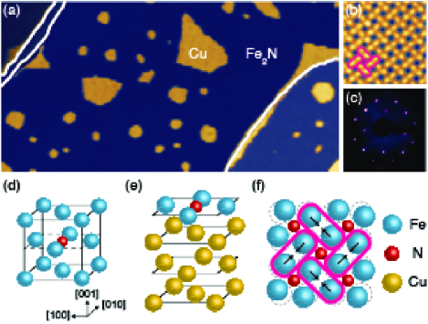
-Fe4N” hereafter. A topographic image of the sample after one growth cycle is shown in
Fig. 1(a). The monolayer -Fe4N is formed on the
Cu terraces at 0.85 ML coverage. An atomically-resolved
image of that surface displayed in
Fig. 1(b) reveals a clear
dimerization of the Fe atoms, typical of ordered
-Fe4N on Cu(001)
Gallego et al. (2005); Takahashi et al. (2016). A LEED
pattern of the surface is shown in
Fig. 1(c), which exhibits sharp spots with the corresponding
symmetry. It is known that
Gallego et al. (2005, 2004b); Navio et al. (2007); Takahashi et al. (2016) the topmost layer of the -Fe4N on
Cu(001) always consists of the Fe2N plane in a bulk Fe4N crystal
shown in Fig. 1(d). A schematic model of the monolayer
-Fe4N is given in Fig. 1(e), composed of
a single Fe2N plane on Cu(001). Accordingly, the surface Fe2N plane takes
reconstruction to the coordination Gallego et al. (2005), in which the Fe
atoms dimerize in two perpendicular directions as illustrated in Fig. 1(f).
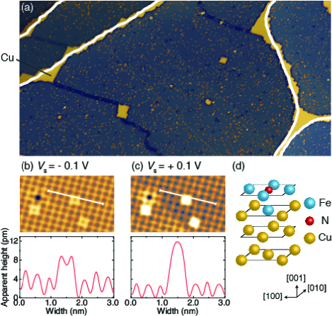
After repeating the growth cycles, we found a new structure different from the monolayer
-Fe4N. Figure 2(a) displays the surface after two
growth cycles in total, namely, another cycle of the N+ ion
bombardment, Fe deposition, and annealing onto the existing
monolayer -Fe4N surface. Then,
the surface
becomes mostly covered with the monolayer -Fe4N, which contains a small
number of bright dots. For a structural
identification of these dots, we measured atomically-resolved topographic
images and line profiles at different as shown in Fig. 2(b) and
2(c). The dot structure imaged at reveals the dimerization of the Fe atoms as the monolayer
-Fe4N surface. This indicates that the topmost part of the dot
consists of the reconstructed Fe2N. At positive of +0.1 V, in contrast, the dot is
recognized as a single protrusion both in the topographic image and line
profile, while the surrounding monolayer -Fe4N still shows
the Fe dimerization. This implies the different electronic structure of the dot
compared to the monolayer -Fe4N, which comes from
the difference in a subsurface atomic structure.
The observed height difference between the dot and the monolayer
-Fe4N ranges from 4 to 10 pm depending on . These values are in the same order of a lattice
mismatch between the bulk crystals of the -Fe4N/Cu(001)
(380 pm) and Cu(001) (362 pm) Gallego et al. (2005), but an order of magnitude smaller than the lattice constant of
the -Fe4N/Cu(001). This
suggests that the topmost layer of the dot is not located above the
monolayer -Fe4N surface, but shares the Fe2N
plane with. Furthermore, the bright
dot is composed of only four pairs of the Fe dimer as imaged in
Fig. 2(b), indicating that the difference in the atomic and/or
electronic structures is restricted within a small area. Considering the
above, it is most plausible that one Fe atom is
embedded just under the surface N atom at the dot center, and thus a bilayer
-Fe4N dot is formed as
schematically shown in Fig. 2(d). This structure corresponds to a
minimum unit of the bilayer -Fe4N on Cu(001).
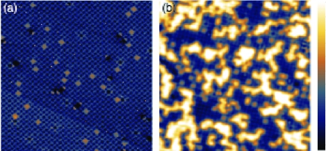
This bilayer dot formed clusters by a further
repetition of the growth cycles. Figure 3(a) shows an enlarged
view of the iron-nitride surface after two growth cycles. The
coverage of the dot is estimated to be 5 % of
the entire surface. Another growth cycle onto this surface led to an
increase in a dot density up to 40 %, as shown in
Fig. 3(b). However, further repetitions of the cycles resulted in neither a
considerable increase in the dot density nor the formation of a continuous bilayer film. This can be attributed to an inevitable sputtering
effect in every growth cycle: an additional N+
ion bombardment to the existing surface not only implanted
N+ ions but also sputtered the surface, which caused the loss
of the iron nitrides already formed at the surface, as well as the increase in the
surface roughness.
To compensate this loss of surface Fe atoms by the sputtering
effect, we also tried to increase the amount of deposited Fe per
cycle. Nonetheless, the number of Fe atoms, which remained at the surface after annealing, did not
increase possibly because of the
thermal metastability of Fe/Cu systems
Detzel and Memmel (1994); Memmel and Detzel (1994); Shen et al. (1995); Bayreuther et al. (1993). The
isolated Fe atoms without any bonding to N atoms were easily
diffused and embedded into the
Cu substrate during the annealing process. As a result, only the imperfect bilayer -Fe4N was obtained
through this method.
III.2 Trilayer -Fe4N film
Multilayer -Fe4N films were obtained by the following procedure. First, the monolayer
-Fe4N was
prepared on Cu(001) as above. Then, 2 ML Fe was deposited under N2 atmosphere (5.010-8 Torr) 111We checked the ionization of nitrogen molecules/atoms without bombardment
using an ion gun. The ion flux monitored for the Fe evaporator increased in proportion to the rise in the N2 pressure, far below
the parameters at which Fe started to be evaporated. This indicates the
ionization of the N2 molecules and/or N atoms around the evaporator possibly by thermal electrons
created inside it. Then, the N+ and N ions could reach to the surface
together with the evaporated Fe atoms, or iron nitride was
already formed before landing. at RT, and the sample was annealed at
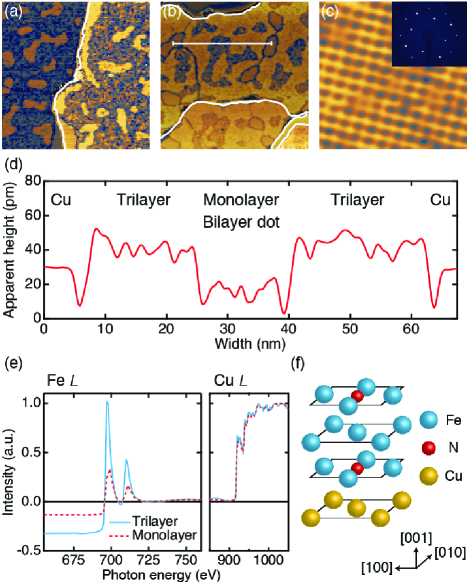
600 K. Figures 4(a) and 4(b) show topographic images
after two and three above mentioned cycles, respectively. In the images, the coverage
of new bright area, different from the imperfect bilayer dot,
monotonously increases with repeating the cycles. A close view of that
new surface is displayed in Fig. 4(c), revealing the dimerized
(or even -like dot) structures. Because a LEED pattern shown in the inset of Fig. 4(c)
exhibits the
symmetry without extra spots, the topmost layer of this surface is
composed of the reconstructed Fe2N plane
Takahashi et al. (2016). Therefore, these observations suggest that the
new area would consist of -Fe4N other than both of the monolayer and bilayer dot.
In order to determine the structure of this newly obtained
-Fe4N, a typical height profile of the surface was recorded as shown in
Fig. 4(d). It is clear that the new structure is higher than both the
Cu surface and the surface including the monolayer/dot-like bilayer
-Fe4N. This suggests that the new area is composed of
-Fe4N thicker than bilayer. Quantitative information on the
thickness of the new structure could be obtained from Fe edge jump spectra shown in Fig. 4(e),
whose intensity is roughly proportional to the amount of
surface/subsurface Fe atoms. The sample
prepared in the same procedure as that shown in Fig. 4(b) reveals an edge jump value of 0.32, while the
monolayer -Fe4N 0.12 222The amount of the Fe
atoms detected in the edge-jump spectra was smaller than that expected
from the initially deposited ones. This implies that a certain amount of Fe
atoms, not participating in forming any -Fe4N structures,
was embedded into the Cu substrate during annealing, at least several nms
(probing depth in the TEY mode) below the surface.. Considering that the new area
occupies 60 % of the entire surface as deduced from
Fig. 4(b), the thickness of this -Fe4N must be less than
quadlayer to meet the experimental edge jump value of 0.32 (See Appendix
A). Hence, the newly
obtained structure is identified as a trilayer -Fe4N
film. An atomic structure expected for
the trilayer -Fe4N on Cu(001) is presented in Fig. 4(f). The
growth without any ion bombardment to the monolayer surface possibly
stabilizes the subsurface pure Fe layer, which
could promote the formation of the
trilayer -Fe4N film in a large area.
Finally, let us mention another growth method of the
-Fe4N film. We previously report a possible layer-by-layer growth of the -Fe4N atomic layers on
Cu(001), by the N+ ion bombardment with a relatively low
energy of 0.15 kV Takagi et al. (2010). This soft
implantation of N+ ions successfully
avoids extra damage to the existing -Fe4N structures
during the repetition of the growth cycles. The reported different electronic/magnetic states could then originate from the difference in the fabrication processes. Another
finding is that, in the current study, only the monolayer and trilayer -Fe4N
could be obtained in a continuous film form. This
implies that an Fe2N-layer termination would be preferable through the present methods, possibly due to
the metastability of an interface between Cu and pure Fe layers Detzel and Memmel (1994); Memmel and Detzel (1994); Shen et al. (1995); Bayreuther et al. (1993).
III.3 Electronic and magnetic properties of -Fe4N atomic layers
The surface
electronic structures of -Fe4N showed large dependence on
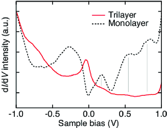
the sample thickness. Figure 5 displays experimental d/d
spectra measured on the surfaces of the
trilayer and monolayer -Fe4N. The
peaks located at +0.20, +0.55, and +0.80 V, mainly originating
from the unoccupied states in the down-spin band characteristic of
Fe local density of states (LDOS), are observed for both the trilayer and monolayer
surfaces. A significant
difference between the spectra is a dominant peak located around observed only for the trilayer surface. This peak possibly originates
from the LDOS peak located around , calculated
for the Fe atoms not bonded to N atoms in the subsurface Fe layer
[corresponding site of Fe4 shown in Fig. 7(b)]. Because of the
orbital character, this peak could be dominantly detected in the STS
spectrum for the trilayer surface. Thus, the appearance of this additional peak could support the different subsurface structure of the trilayer sample,
especially, the existence of the subsurface Fe layer proposed
above.
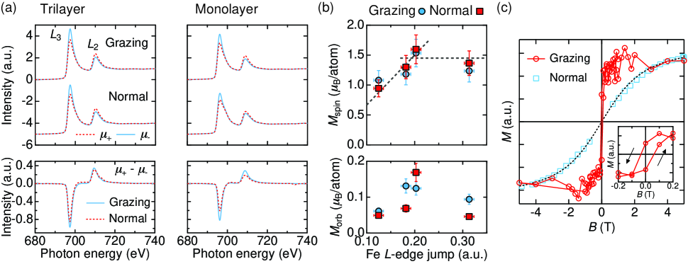
The entire electronic and magnetic
properties of the sample, including both surface and subsurface information, were investigated by using XAS and XMCD techniques at the
Fe absorption edges. Figure
6(a) shows XAS () and XMCD
() spectra under of the trilayer and monolayer samples in the grazing
() and normal incidence (). Here,
denotes a x-ray absorption spectrum with the photon helicity parallel (antiparallel) to the Fe 3
majority spin, and an incident angle is
defined as that between the sample normal and incident x-ray. The
trilayer (monolayer) sample was prepared in the same procedure as that
shown in Fig. 4(b) [Fig. 1(a)]. It is clear that the XMCD intensity is larger in the trilayer
one, indicating an enhancement of magnetic moments with increasing
thickness.
For a further quantitative analysis on the magnetic moments, we applied
XMCD sum rules Carra et al. (1993); Thole et al. (1992)
to the obtained spectra and estimated spin () and orbital
() magnetic moments separately. Note that the average number of 3
holes () of 3.2 was used in the sum-rule analysis, which
was estimated by comparing the area of the experimental XAS spectra with that of a reference spectrum of
bcc Fe/Cu(001) () Chen et al. (1995). The
thickness dependence of the and values is
summarized in Fig. 6(b). The value of increases
monotonously with increasing the Fe -edge jump value, namely, an
average sample thickness, and finally saturates
at /atom in the trilayer sample (corresponding
edge jump value of 0.32). The change in is not so
systematic relative to , however, the values
seem to be enhanced in the
grazing incidence. This implies
an in-plane easy magnetization of the -Fe4N atomic layers on
Cu(001), also consistent with the previous reports on the
-Fe4N thin films on Cu(001) Gallego et al. (2004a); Takagi et al. (2010). Figure 6(c) shows magnetization curves of the
monolayer sample, whose intensity corresponds to the -peak XAS intensity normalized to the one. The curve
recorded in the normal incidence shows negligible remanent
magnetization. On the other hand, that in the grazing one draws a
rectangular hysteresis loop, which confirms the in-plane easy magnetization. The coercivity
of the monolayer sample is estimated to be 0.05 T at 8.0 K, larger
than 0.01 T for 5 ML Fe/Cu(001)
Li et al. (1994), 1 mT for 5 ML
Fe/GaAs(100)-(46) Xu et al. (1998) and the 30 nm
thick -Fe4N film Gallego et al. (2004a) at RT.
III.4 Theoretical analysis on the electronic and magnetic states of -Fe4N atomic layers on Cu(001)
| Surface Fe2N | Subsurface Fe | Interfacial Fe2N | ||||
| Fe1 | Fe2 | Fe3 | Fe4 | Fe5 | Fe6 | |
| Monolayer | 1.1 | 1.1 | - | - | - | - |
| Trilayer | 1.8 | 1.8 | 2.0 | 3.0 | 0.62 | 0.62 |
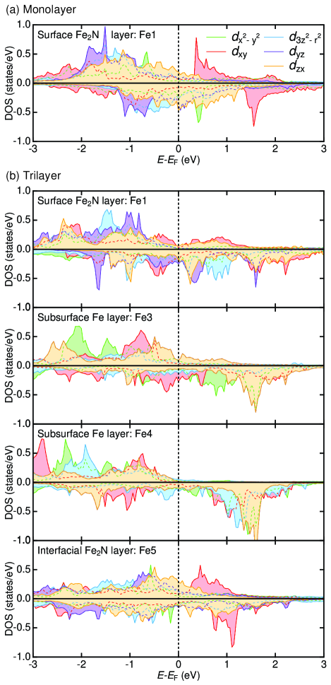
The observed thickness dependence of the magnetic moments can be
well understood with a help of first-principles calculations. Figures 7(a)
and 7(b) show layer-resolved DOS of the monolayer and trilayer
-Fe4N on Cu(001), respectively. Here, non-equivalent Fe sites in
each layer are distinguished by different numbering. In particular, the Fe atoms at the Fe3 (Fe4) site in the trilayer
-Fe4N correspond to those with (without) a bond to
N atoms 333The difference of
DOS between (Fe1, Fe2) in the monolayer -Fe4N, (Fe1,
Fe2) and (Fe5, Fe6) in the trilayer one is just a switch of the orbital
assignment between and . Therefore, the DOS of
Fe2 in the monolayer -Fe4N, Fe2 and Fe6 in the
trilayer one is not presented here.. In Table 1,
calculated values of an atomic magnetic moment , corresponding to
+ along the easy magnetization direction, are also listed. In the monolayer case, the
calculated is 1.1 /atom, which is in perfect
agreement with the experimental value. This supports an ideal
atomic structure of our monolayer sample.
Interestingly, the value of for the Fe atoms in the
monolayer -Fe4N is more than 1.5 times smaller than
that in the topmost layer of the
trilayer one (1.83 /atom). In comparison with the DOS shown at the top of
Fig. 7(b), the impact of the hybridization with the Cu states
on the Fe DOS can be seen in Fig. 7(a): First, the DOS in the
up-spin band, especially with and orbitals, becomes
to have a tail toward a higher-energy side across the . This
change deviates the 3 electrons in the up-spin band from a
fully-occupied nature. Moreover, the spin asymmetry of the occupied 3
electrons, the difference between the electron occupation into each spin band
normalized by the sum of them, reduces especially for the DOS with
, and orbitals. These changes could decrease of the Fe atoms. Note that the similar reduction in the magnetic
moments of 3 TMs due to the hybridization with Cu states is
reported, for example, in
Ref. Tersoff and Falicov, 1982; Hjortstam et al., 1996.
Then, by comparing two different
Fe2N interfaces with the Cu substrate, it turns out that of the
monolayer -Fe4N (1.1 /atom) is almost twice compared to
that of the trilayer one (0.62 /atom). In the monolayer case, the Fe2N layer faces to a vacuum and the
Fe atoms are under reduced atomic coordination. This results in the narrower
band width, and thus the DOS intensity increases in the
vicinity of . Accordingly, a larger exchange splitting can be
possible and the spin asymmetry of the occupied 3 electrons increases as shown in Fig. 7(a), compared to the interfacial Fe2N layer of the trilayer
-Fe4N [bottom panel of Fig. 7(b)]. This leads to larger magnetic
moments at the surface. As a result, the competition between
the enhancement at the surface and the
decrease at the interface would make values quite layer-sensitive.
In the subsurface Fe layer of
the trilayer -Fe4N, the value of becomes
largest due to the bulk coordination of the Fe atoms. Especially the Fe atoms not
bonded to the N ones possess of 3.0 /atom,
which is comparable to the values of Fe atoms at the same site in the
bulk -Fe4N Frazer (1958). Consequently, by averaging the
layer-by-layer values of the trilayer
-Fe4N, the total magnetic moment
detected in the XMCD measurement is expected to be 1.7 /Fe, with the electron escape depth taken into account (See Appendix
A). Considering the composition expected to the trilayer
sample, this value can well explain the experimental one of 1.5 /Fe.
The theory also demonstrates the direction of an easy magnetization
axis. The in-plane easy magnetization of
our -Fe4N samples was confirmed by the magnetization
curves as well as the incidence
dependence of the value. In contrast, the pristine ultrathin Fe
films, which form either fct or fcc structures on Cu(001), show uncompensated
out-of-plane spins over a few surface layers
Pescia et al. (1987); Meyerheim et al. (2009). This shift
of magnetic anisotropy by nitridation can be understood from the orbital-resolved Fe DOS shown in Figs. 7(a) and 7(b). Unlike
the pure Fe/Cu(001) system Lorenz and Hafner (1996), the occupation of 3 electrons in states with out-of-plane-oriented orbitals () is considerably larger than that with
in-plane-oriented ones (). This could make prefer to align
within a film plane, resulting in the in-plane magnetization of the system
Bruno (1989).
IV Summary
In conclusion, we have conducted a detailed study on the growth,
electronic and magnetic properties of the -Fe4N atomic layers on
Cu(001). The ordered trilayer film of -Fe4N can be
prepared by the Fe deposition under N2 atmosphere onto the existing monolayer surface. On the other hand, the repetition of
the growth cycles including the high-energy N+ ion implantation
resulted in the imperfect bilayer -Fe4N. The STM and STS observations revealed the change in the surface topography
and electronic structures with increasing the sample thickness. The XAS
and XMCD measurements also showed the thickness dependence of the spectra, and the corresponding
evolution of the values. All the thickness
dependence of the electronic and magnetic properties is well explained
by the layer-resolved DOS calculated using the first
principles. Structural perfection of the system makes it possible
to fully comprehend the layer-by-layer electronic/magnetic states of the -Fe4N atomic layers.
V Acknowledgement
This work was partly supported by the JSPS Grant-in-Aid for Young Scientists (A), Grant No. 16H05963, for Scientific Research (B),
Grant No. 26287061, the Hoso Bunka Foundation, Shimadzu Science
Foundation, Iketani Science and Technology Foundation, and
Nanotechnology Platform Program (Molecule and Material Synthesis) of the
Ministry of Education, Culture, Sports, Science and Technology (MEXT),
Japan. Y. Takahashi was supported by
the Grant-in-Aid for JSPS Fellows and the Program for Leading Graduate
Schools (MERIT). A.E. acknowledges funding by the German Research
Foundation (DFG Grants No. ER 340/4-1).
Appendix A Conversion of XAS edge jump values to the thickness of -Fe4N
The escape probability of electrons from inside a sample to a vacuum depends on the depth at which the electrons are excited. For a numerical interpretation of the XAS edge jump, the following factors should be mainly considered in principle: the penetration length of an incident x-ray () and electron escape depth (), both energy-dependent. In the case of a few atomic layers of 3 transition metals, the attenuation of the incident x-ray intensity is almost negligible because is orders of magnitude longer than the sample thickness Nakajima et al. (1999). Therefore, in the present case, only the electron escape probability at the depth from the surface, namely, a factor of is taken into account. As for the value of Fe, 17 Å was tentatively assumed in our analysis, which is experimentally determined for Fe thin films Nakajima et al. (1999). Then, based on the experimental Fe (N) edge jump values of 0.12 (0.015), those for the full-coverage dot-like bilayer, trilayer, and quadlayer -Fe4N on Cu(001) are calculated as summarized in Table 2.
| Fe edge jump | N edge jump | |||
|---|---|---|---|---|
| Experiment | Calculation | Experiment | Calculation | |
| Monolayer | 0.12 (exp.) | 0.015 (exp.) | ||
| Bilayer dot | - | 0.19 | - | 0.015 |
| Trilayer | 0.32 | 0.40 | 0.032 | 0.034 |
| Quadlayer | - | 0.57 | - | 0.034 |
References
- Coey and Smith (1999) J. Coey and P. Smith, J. Magn. Magn. Mater. 200, 405 (1999).
- Frazer (1958) B. C. Frazer, Phys. Rev. 112, 751 (1958).
- Coey (1994) J. M. D. Coey, J. Appl. Phys. 76, 6632 (1994).
- Komuro et al. (1990) M. Komuro, Y. Kozono, M. Hanazono, and Y. Sugita, J. Appl. Phys. 67, 5126 (1990).
- Ortiz et al. (1994) C. Ortiz, G. Dumpich, and A. H. Morrish, Appl. Phys. Lett. 65, 2737 (1994).
- Atiq et al. (2008) S. Atiq, H.-S. Ko, S. A. Siddiqi, and S.-C. Shin, Appl. Phys. Lett. 92, 222507 (2008).
- Borsa et al. (2001) D. M. Borsa, S. Grachev, D. O. Boerma, and J. W. J. Kerssemakers, Appl. Phys. Lett. 79, 994 (2001).
- Gallego et al. (2004a) J. M. Gallego, S. Y. Grachev, D. M. Borsa, D. O. Boerma, D. Écija, and R. Miranda, Phys. Rev. B 70, 115417 (2004a).
- Ito et al. (2011) K. Ito, G. H. Lee, K. Harada, M. Suzuno, T. Suemasu, Y. Takeda, Y. Saitoh, M. Ye, A. Kimura, and H. Akinaga, Appl. Phys. Lett. 98, 102507 (2011).
- Nikolaev et al. (2003) K. R. Nikolaev, I. N. Krivorotov, E. D. Dahlberg, V. A. Vas’ko, S. Urazhdin, R. Loloee, and W. P. Pratt, Appl. Phys. Lett. 82, 4534 (2003).
- Kokado et al. (2006) S. Kokado, N. Fujima, K. Harigaya, H. Shimizu, and A. Sakuma, Phys. Rev. B 73, 172410 (2006).
- Ito et al. (2015) K. Ito, K. Toko, Y. Takeda, Y. Saitoh, T. Oguchi, T. Suemasu, and A. Kimura, J. Appl. Phys. 117, 193906 (2015).
- Fang et al. (2014) C.-M. Fang, R. S. Koster, W.-F. Li, and M. A. van Huis, RSC Adv. 4, 7885 (2014).
- Kim et al. (1997) S. H. Kim, K. S. Lee, H. G. Min, J. Seo, S. C. Hong, T. H. Rho, and J.-S. Kim, Phys. Rev. B 55, 7904 (1997).
- Nouvertné et al. (1999) F. Nouvertné, U. May, M. Bamming, A. Rampe, U. Korte, G. Güntherodt, R. Pentcheva, and M. Scheffler, Phys. Rev. B 60, 14382 (1999).
- Torelli et al. (2003) P. Torelli, F. Sirotti, and P. Ballone, Phys. Rev. B 68, 205413 (2003).
- Srivastava et al. (1997) P. Srivastava, N. Haack, H. Wende, R. Chauvistré, and K. Baberschke, Phys. Rev. B 56, R4398 (1997).
- Farle et al. (1997a) M. Farle, W. Platow, A. N. Anisimov, P. Poulopoulos, and K. Baberschke, Phys. Rev. B 56, 5100 (1997a).
- Farle et al. (1997b) M. Farle, B. Mirwald-Schulz, A. N. Anisimov, W. Platow, and K. Baberschke, Phys. Rev. B 55, 3708 (1997b).
- Schulz and Baberschke (1994) B. Schulz and K. Baberschke, Phys. Rev. B 50, 13467 (1994).
- Li et al. (1994) D. Li, M. Freitag, J. Pearson, Z. Q. Qiu, and S. D. Bader, Phys. Rev. Lett. 72, 3112 (1994).
- Straub et al. (1996) M. Straub, R. Vollmer, and J. Kirschner, Phys. Rev. Lett. 77, 743 (1996).
- Weber et al. (1996) W. Weber, A. Bischof, R. Allenspach, C. H. Back, J. Fassbender, U. May, B. Schirmer, R. M. Jungblut, G. Güntherodt, and B. Hillebrands, Phys. Rev. B 54, 4075 (1996).
- Meyerheim et al. (2009) H. L. Meyerheim, J.-M. Tonnerre, L. Sandratskii, H. C. N. Tolentino, M. Przybylski, Y. Gabi, F. Yildiz, X. L. Fu, E. Bontempi, S. Grenier, and J. Kirschner, Phys. Rev. Lett. 103, 267202 (2009).
- Gejo et al. (2003) T. Gejo, Y. Takata, T. Hatsui, M. Nagasono, H. Oji, N. Kosugi, and E. Shigemasa, Chem. Phys. 289, 15 (2003).
- Nakagawa et al. (2008) T. Nakagawa, Y. Takagi, Y. Matsumoto, and T. Yokoyama, Jpn. J. Appl. Phys. 47, 2132 (2008).
- Perdew and Wang (1992) J. P. Perdew and Y. Wang, Phys. Rev. B 45, 13244 (1992).
- Lüders et al. (2001) M. Lüders, A. Ernst, W. M. Temmerman, Z. Szotek, and P. J. Durham, J. Phys.: Condens. Matter 13, 8587 (2001).
- Geilhufe et al. (2015) M. Geilhufe, S. Achilles, M. A. Köbis, M. Arnold, I. Mertig, W. Hergert, and A. Ernst, J. Phys.: Condens. Matter 27, 435202 (2015).
- Gallego et al. (2005) J. M. Gallego, D. O. Boerma, R. Miranda, and F. Ynduráin, Phys. Rev. Lett. 95, 136102 (2005).
- Takahashi et al. (2016) Y. Takahashi, T. Miyamachi, K. Ienaga, N. Kawamura, A. Ernst, and F. Komori, Phys. Rev. Lett. 116, 056802 (2016).
- Gallego et al. (2004b) J. M. Gallego, S. Y. Grachev, M. C. G. Passeggi, F. Sacharowitz, D. Ecija, R. Miranda, and D. O. Boerma, Phys. Rev. B 69, 121404 (2004b).
- Navio et al. (2007) C. Navio, J. Alvarez, M. J. Capitan, D. Ecija, J. M. Gallego, F. Yndurain, and R. Miranda, Phys. Rev. B 75, 125422 (2007).
- Detzel and Memmel (1994) T. Detzel and N. Memmel, Phys. Rev. B 49, 5599 (1994).
- Memmel and Detzel (1994) N. Memmel and T. Detzel, Surf. Sci. 307, 490 (1994).
- Shen et al. (1995) J. Shen, J. Giergiel, A. Schmid, and J. Kirschner, Surf. Sci. 328, 32 (1995).
- Bayreuther et al. (1993) G. Bayreuther, F. den Broeder, D. Chambliss, K. Johnson, R. Wilson, and S. Chiang, J. Magn. Magn. Mater. 121, 1 (1993).
- Note (1) We checked the ionization of nitrogen molecules/atoms without bombardment using an ion gun. The ion flux monitored for the Fe evaporator increased in proportion to the rise in the N2 pressure, far below the parameters at which Fe started to be evaporated. This indicates the ionization of the N2 molecules and/or N atoms around the evaporator possibly by thermal electrons created inside it. Then, the N+ and N ions could reach to the surface together with the evaporated Fe atoms, or iron nitride was already formed before landing.
- Note (2) The amount of the Fe atoms detected in the edge-jump spectra was smaller than that expected from the initially deposited ones. This implies that a certain amount of Fe atoms, not participating in forming any -Fe4N structures, was embedded into the Cu substrate during annealing, at least several nms (probing depth in the TEY mode) below the surface.
- Takagi et al. (2010) Y. Takagi, K. Isami, I. Yamamoto, T. Nakagawa, and T. Yokoyama, Phys. Rev. B 81, 035422 (2010).
- Carra et al. (1993) P. Carra, B. T. Thole, M. Altarelli, and X. Wang, Phys. Rev. Lett. 70, 694 (1993).
- Thole et al. (1992) B. T. Thole, P. Carra, F. Sette, and G. van der Laan, Phys. Rev. Lett. 68, 1943 (1992).
- Chen et al. (1995) C. T. Chen, Y. U. Idzerda, H.-J. Lin, N. V. Smith, G. Meigs, E. Chaban, G. H. Ho, E. Pellegrin, and F. Sette, Phys. Rev. Lett. 75, 152 (1995).
- Xu et al. (1998) Y. B. Xu, E. T. M. Kernohan, D. J. Freeland, A. Ercole, M. Tselepi, and J. A. C. Bland, Phys. Rev. B 58, 890 (1998).
- Note (3) The difference of DOS between (Fe1, Fe2) in the monolayer -Fe4N, (Fe1, Fe2) and (Fe5, Fe6) in the trilayer one is just a switch of the orbital assignment between and . Therefore, the DOS of Fe2 in the monolayer -Fe4N, Fe2 and Fe6 in the trilayer one is not presented here.
- Tersoff and Falicov (1982) J. Tersoff and L. M. Falicov, Phys. Rev. B 26, 6186 (1982).
- Hjortstam et al. (1996) O. Hjortstam, J. Trygg, J. M. Wills, B. Johansson, and O. Eriksson, Phys. Rev. B 53, 9204 (1996).
- Pescia et al. (1987) D. Pescia, M. Stampanoni, G. L. Bona, A. Vaterlaus, R. F. Willis, and F. Meier, Phys. Rev. Lett. 58, 2126 (1987).
- Lorenz and Hafner (1996) R. Lorenz and J. Hafner, Phys. Rev. B 54, 15937 (1996).
- Bruno (1989) P. Bruno, Phys. Rev. B 39, 865 (1989).
- Nakajima et al. (1999) R. Nakajima, J. Stöhr, and Y. U. Idzerda, Phys. Rev. B 59, 6421 (1999).