Gate-Defined One-Dimensional Channel and Broken Symmetry States in MoS2 van der Waals Heterostructures
Abstract
We have realized encapsulated trilayer MoS2 devices with gated graphene contacts. In the bulk, we observe an electron mobility as high as 7000 cm2/(V s) at a density of 3 1012 cm-2 at a temperature of 1.9 K. Shubnikov–de Haas oscillations start at magnetic fields as low as 0.9 T. The observed 3-fold Landau level degeneracy can be understood based on the valley Zeeman effect. Negatively biased split gate electrodes allow us to form a channel that can be completely pinched off for sufficiently large gate voltages. The measured conductance displays plateau-like features.
Laterally confined two-dimensional (2D) materials offer the opportunity to engineer quantum states with tunable spin, charge and even valley degrees of freedomHanson et al. (2007); Loss and DiVincenzo (1998); Petta et al. (2005). The pure thinness of these materials in combination with 2D insulators such as boron nitride pave the way for ultrasmall strongly coupled gate-defined quantum devicesGoossens et al. (2012); Song et al. (2015); Wang et al. ; Novoselov et al. (2005). In addition the variety of transition metal dichalcogenides (TMDCs) materials will allow to choose different strength of spin-orbit interaction that is relevant for electric control of spin and valley-states in view of quantum information processing. In this Letter, we describe a split gate geometry realized on a high-quality molybdenum disulfide (MoS2) van der Waals heterostructure that results in a tunable tunneling barrier, the starting point for any electronic quantum device. The electronic quality of our trilayer MoS2 device is documented by the observation of Shubnikov-de Haas oscillations (SdHO) occurring at magnetic fields as low as 0.9 T. In addition a 3-fold degeneracy of the Landau levels (LLs) is observed arising from the 3 Q and 3 Q’ valleys situated in the middle of the Brillouin zone and shifted in magnetic field by the valley Zeeman effectLi et al. (2014); Srivastava et al. (2015); MacNeill et al. (2015); Aivazian et al. (2015); Wu et al. (2016). The constriction can be completely pinched off with resistances values exceeding the quantum of resistance by orders of magnitude, a prerequisite for the realization of any single-electron transistor. We observe the occurrence of plateau-like features in the conductance with a spacing of the order of . These experiments are a first step toward gate controlled quantum devices in transition metal dichalcogenides.
To achieve high mobility TMDC devices, we fabricate MoS2-based van der Waals heterostructures. As shown schematically in Figure 1a, a trilayer MoS2 flake ( 2 nm thick), contacted with two few-layer graphene (FLG) sheets, is encapsulated between hexagonal boron nitride (hBN) crystalsLee et al. (2015); Cui et al. (2015); Liu et al. (2015). The bottom one is 30 nm thick and separates the MoS2 from substrate phonons and charged impurities, further serving as an atomically flat substrateXue et al. (2011). The top one is 20 nm thick and prevents the adsorption of organic residues during the fabrication process. To assemble the heterostructure we employ a polymer-based dry pick-up and transfer techniqueWang et al. (2013, 2015) using a polycarbonate filmZomer et al. (2014); Bretheau et al. (2017) supported by polydimethylsiloxane. Assembling and exfoliating the various thin films was performed in an argon environmentCao et al. (2015). The films’ thicknesses were first determined from the optical contrast and then verified by atomic force microscopy (AFM). The top hBN crystal serves as the dielectric layer for the top gates whereas the SiO2/n-Si substrate works as the bottom dielectric (285 nm) and gate electrode. The top gate structure consists of two pairs of local gates on top of the contact areas between graphene and MoS2, and a split gate with a 100 nm gap (Figure 1c). In order to avoid electrostatic inhomogeneities, the split gate has been deposited on a bubble-free area on top of the MoS2 channel, found by AFM. Cr/Au electrodes are used as one-dimensional edge contacts to graphene (red dashed lines in Figure 1b)Wang et al. (2013). Finally, the four-terminal device geometry is defined by etching through the top hBN, MoS2 and FLG (Figure 1b). As shown in Figure 1a, we can tune the carrier density in the MoS2 channel by biasing the Si gate electrode (). We can further tune locally the carrier density in the contact area between MoS2 and graphene () and deplete the MoS2 two-dimensional electron gas (2DEG) ().
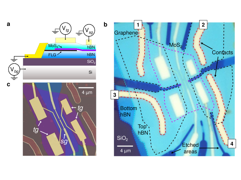
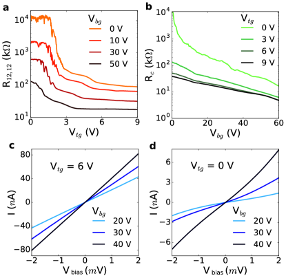
Figure 2a shows the low temperature ( K) two-terminal resistance as a function of , for different . The resistance decreases with increasing , as expected for an n-type semiconductorCui et al. (2015). At fixed , the resistance drops for increasing by up to 2 orders of magnitude. Figure 2b displays the estimated contact resistance , where is the two-probe resistance and is the four-probe resistance of MoS2 (Figure 1b). can be improved by up to 3 orders of magnitude with increasing . Figure 2c,d shows the current flowing into the device () as a function of the voltage applied between two graphene electrodes (). When V, non linear curves are observed indicating gapped-behavior corresponding to nonohmic contacts (Figure 2d). Linear behavior is achieved at higher as already demonstrated in previous worksLee et al. (2015); Cui et al. (2015); Liu et al. (2015). We observe linear curves at any V when V (Figure 2b). Therefore, we can locally tune the carrier density in the MoS2 layer and the Fermi level of graphene to achieve ohmic contact without compromising the low carrier density in the MoS2 channel. This allows us to investigate the physics of MoS2 at the edge of the conduction band.
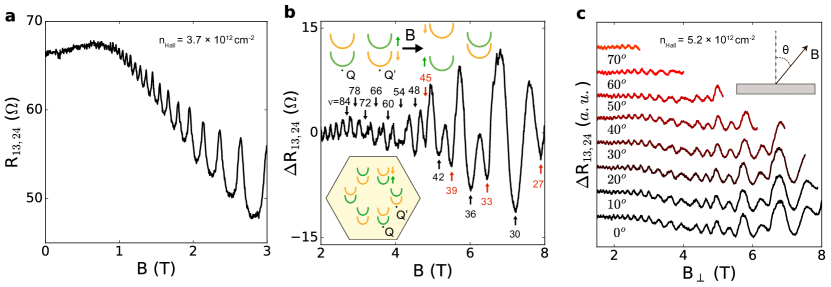
To examine the quality of our device we performed magnetotransport measurements at K. Four-probe measurements, using the standard lock-in technique at 80.31 Hz, can be performed due to the reasonably good ohmic contacts. Figure 3a shows the four-terminal resistance as a function of the magnetic field , at cm-2 . We observe SdHO starting at T, which yields a lower boundary for the quantum mobility of about 11000 cm2/Vs, in agreement with the measured van der Pauw mobility of 7000 cm2/Vs. Figure 3b displays four-terminal resistance with a smooth background subtracted, as a function of , at cm-2. Distinctive features appear above T on top of the SdHO. They first emerge as shoulder-like features developing then into local minima in the SdHO as shown in Figure 3b with red arrows. From the SdHO we can determine the density of the 2DEG, where is the period of the SdHO and the prefactor accounts for spin and valley degeneracies. The electron density calculated from SdHO matches the Hall density when . As shown in Figure 3b, a 6-fold LL degeneracy is clearly observed at relatively low magnetic field. Above T additional minima for filling factors 27, 33, 39 and 45 appear. The degeneracy of 6 arises from the 3 Q and 3 Q’ valleys located along symmetry lines in the first Brillouin zone (inset of Fig. 3b), which correspond to the 6 degenerate conduction band minima expected from the band structure calculations of trilayer MoS2Cheiwchanchamnangij and Lambrecht (2012); Wang et al. (2012); Mak et al. (2010); Cappelluti et al. (2013); Chhowalla et al. (2013); Wu et al. (2016). The spin degeneracy within each Q and Q’ valley is already lifted by broken inversion and time reversal symmetry. At relatively high magnetic fields, due to the opposite spin character at Q and Q’ valley in 2D TMDCXiao et al. (2012); Chhowalla et al. (2013), the Zeeman splitting becomes comparable to the LL splitting and we observe the LL sextet being lifted into two LL triplets (inset of Figure 3b). Figure 3c shows as a function of the magnetic field component perpendicular to the 2DEG plane () at different angles (inset of Figure 3c). The SdHOs remain unchanged for all values of up to 70∘. A similar behavior was observed for mono- and bilayer WSe2Movva et al. . The insensitivity of the Zeeman energy to the parallel component of the magnetic field may indicate that the electron spin is locked perpendicular to the plane due to the strong spin-orbit coupling and broken inversion symmetry in trilayer MoS2Wu et al. (2016).
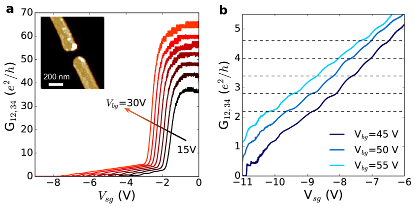
High-quality MoS2 2DEGs allow us to investigate quantum transport in gate-defined nanostructures. As shown in the inset of Figure 4a, we define a constriction, 100 nm wide and 200 nm long, by electrostatically depleting the MoS2 layer. In Figure 4a, we display the measured four-terminal conductance in unit of the conductance quantum,Wharam et al. (1988); van Wees et al. (1988) , as a function of and , at K. At higher electron density, that is, higher , a more negative is required in order to pinch off the MoS2 channel with on-off ratios exceeding . Figure 4b shows , close to pinch-off, at different . At relatively high carrier density ( cm-2, Figure 4b), we observe a significant decrease of resonances close to pinch-off, which we attribute to localized states forming in the electrostatically confined channel. These states, caused by the disorder potential in the MoS2, may be better screened at high carrier density. At T, we observe even-spaced plateau-like features within 2 and 5 . While plateau-like features are expected at multiples of 6e2/h, the experimental results show features that are roughly spaced by e2/h, and even these values are not met precisely. Level degeneracies might be lifted by the additional confinement of the quantum point contact. However, we do not know the exact reason why the experimental data show plateau-like features that match only qualitatively a quantization with values around multiples of e2/h. Further improvement of the 2DEG quality is required to demonstrate exact conductance quantization. Figure 4b shows raw data for the conductance. Subtracting a series resistance to account for possible contributions of the surrounding areas of the electron gas did not lead to a better matching of the plateau-like features with the expected values of the conductance quantization.
In conclusion, we have developed a van der Waals heterostructure platform that allows us to obtain high-quality 2DEGs in MoS2, displaying an electron mobility of cm2/(V s) with electron density as low as 1012 cm-2. We observe SdHO starting at magnetic fields as low as 0.9 T with a 6-fold LL degeneracy that is lifted into a 3-fold LL with magnetic field. We further observe signatures of quantized conductance by electrostatically depleting a split gate on the MoS2 2DEG. The realization of an electrostatically tunable tunneling barrier reaching full pinch-off is the first step toward gate-defined quantum dots in 2D semiconducting TMDC in order to control and manipulate the spin and valley states of single confined electrons.Novoselov et al. (2016); Kormányos et al. (2014); Loss and DiVincenzo (1998)
During preparation of the manuscript, we became aware of related works.Epping et al. ; Wang et al.
acknowledgement
We thank Guido Burkard, Andras Kis, Matija Karalic and Christopher Mittag for fruitful discussions. We acknowledge financial support by the Graphene Flagship, the EU Spin-Nano RTN network, and by the National Center of Competence in Research on Quantum Science and Technology (NCCR QSIT) funded by the Swiss National Science Foundation. Growth of hexagonal boron nitride crystals was supported by the Elemental Strategy Initiative conducted by the MEXT, Japan and JSPS KAKENHI Grant Numbers JP15K21722.
References
- Hanson et al. (2007) R. Hanson, L. P. Kouwenhoven, J. R. Petta, S. Tarucha, and L. M. K. Vandersypen, Rev. Mod. Phys. 79, 1217 (2007).
- Loss and DiVincenzo (1998) D. Loss and D. P. DiVincenzo, Phys. Rev. A 57, 120 (1998).
- Petta et al. (2005) J. R. Petta, A. C. Johnson, J. M. Taylor, E. A. Laird, A. Yacoby, M. D. Lukin, C. M. Marcus, M. P. Hanson, and A. C. Gossard, Science 309, 2180 (2005).
- Goossens et al. (2012) A. S. M. Goossens, S. C. M. Driessen, T. A. Baart, K. Watanabe, T. Taniguchi, and L. M. K. Vandersypen, Nano Lett. 12, 4656 (2012).
- Song et al. (2015) X.-X. Song, D. Liu, V. Mosallanejad, J. You, T.-Y. Han, D.-T. Chen, H.-O. Li, G. Cao, M. Xiao, G.-C. Guo, and et al., Nanoscale 7, 16867 (2015).
- (6) K. Wang, T. Taniguchi, K. Watanabe, and P. Kim, arXiv:1610.02929 .
- Novoselov et al. (2005) K. S. Novoselov, D. Jiang, F. Schedin, T. J. Booth, V. V. Khotkevich, S. V. Morozov, and A. K. Geim, Proc. Natl. Acad. Sci. U. S. A. 102, 10451 (2005).
- Li et al. (2014) Y. Li, J. Ludwig, T. Low, A. Chernikov, X. Cui, G. Arefe, Y. D. Kim, A. M. van der Zande, A. Rigosi, H. M. Hill, and et al., Phys. Rev. Lett. 113, 266804 (2014).
- Srivastava et al. (2015) A. Srivastava, M. Sidler, A. V. Allain, D. S. Lembke, A. Kis, and A. Imamoğlu, Nat. Phys. 11, 141 (2015).
- MacNeill et al. (2015) D. MacNeill, C. Heikes, K. F. Mak, Z. Anderson, A. Kormányos, V. Zólyomi, J. Park, and D. C. Ralph, Phys. Rev. Lett. 114, 037401 (2015).
- Aivazian et al. (2015) G. Aivazian, Z. Gong, A. M. Jones, R.-L. Chu, J. Yan, D. G. Mandrus, C. Zhang, D. Cobden, W. Yao, and X. Xu, Nat. Phys. 11, 148 (2015).
- Wu et al. (2016) Z. Wu, S. Xu, H. Lu, A. Khamoshi, G.-B. Liu, T. Han, Y. Wu, J. Lin, G. Long, Y. He, and et al., Nat. Commun. 7, 12955 (2016).
- Lee et al. (2015) G.-H. Lee, X. Cui, Y. D. Kim, G. Arefe, X. Zhang, C.-H. Lee, F. Ye, K. Watanabe, T. Taniguchi, P. Kim, and et al., ACS Nano 9, 7019 (2015).
- Cui et al. (2015) X. Cui, G.-H. Lee, Y. D. Kim, G. Arefe, P. Y. Huang, C.-H. Lee, D. A. Chenet, X. Zhang, L. Wang, F. Ye, and et al., Nat. Nanotechnol. 10, 534 (2015).
- Liu et al. (2015) Y. Liu, H. Wu, H.-C. Cheng, S. Yang, E. Zhu, Q. He, M. Ding, D. Li, J. Guo, N. O. Weiss, and et al., Nano Lett. 15, 3030 (2015).
- Xue et al. (2011) J. Xue, J. Sanchez-Yamagishi, D. Bulmash, P. Jacquod, A. Deshpande, K. Watanabe, T. Taniguchi, P. Jarillo-Herrero, and B. J. LeRoy, Nat. Mater. 10, 282 (2011).
- Wang et al. (2013) L. Wang, I. Meric, P. Y. Huang, Q. Gao, Y. Gao, H. Tran, T. Taniguchi, K. Watanabe, L. M. Campos, D. A. Muller, and et al., Science 342, 614 (2013).
- Wang et al. (2015) J. I.-J. Wang, Y. Yang, Y.-A. Chen, K. Watanabe, T. Taniguchi, H. O. H. Churchill, and P. Jarillo-Herrero, Nano Lett. 15, 1898 (2015).
- Zomer et al. (2014) P. J. Zomer, M. H. D. Guimarães, J. C. Brant, N. Tombros, and B. J. van Wees, Appl. Phys. Lett. 105, 013101 (2014).
- Bretheau et al. (2017) L. Bretheau, J. I.-J. Wang, R. Pisoni, K. Watanabe, T. Taniguchi, and P. Jarillo-Herrero, Nat. Phys. advance online publication (2017), 10.1038/nphys4110.
- Cao et al. (2015) Y. Cao, A. Mishchenko, G. L. Yu, E. Khestanova, A. P. Rooney, E. Prestat, A. V. Kretinin, P. Blake, M. B. Shalom, C. Woods, and et al., Nano Lett. 15, 4914 (2015).
- Cheiwchanchamnangij and Lambrecht (2012) T. Cheiwchanchamnangij and W. R. L. Lambrecht, Phys. Rev. B 85, 205302 (2012).
- Wang et al. (2012) Q. H. Wang, K. Kalantar-Zadeh, A. Kis, J. N. Coleman, and M. S. Strano, Nat. Nanotechnol. 7, 699 (2012).
- Mak et al. (2010) K. F. Mak, C. Lee, J. Hone, J. Shan, and T. F. Heinz, Phys. Rev. Lett. 105, 136805 (2010).
- Cappelluti et al. (2013) E. Cappelluti, R. Roldán, J. A. Silva-Guillén, P. Ordejón, and F. Guinea, Phys. Rev. B 88, 075409 (2013).
- Chhowalla et al. (2013) M. Chhowalla, H. S. Shin, G. Eda, L.-J. Li, K. P. Loh, and H. Zhang, Nat. Chem. 5, 263 (2013).
- Xiao et al. (2012) D. Xiao, G.-B. Liu, W. Feng, X. Xu, and W. Yao, Phys. Rev. Lett. 108, 196802 (2012).
- (28) H. C. P. Movva, B. Fallahazad, K. Kim, S. Larentis, T. Taniguchi, K. Watanabe, S. K. Banerjee, and E. Tutuc, arXiv:1702.05166 .
- Wharam et al. (1988) D. A. Wharam, T. J. Thornton, R. Newbury, M. Pepper, H. Ahmed, J. E. F. Frost, D. G. Hasko, D. C. Peacock, D. A. Ritchie, and G. A. C. Jones, J. of Phys. C: Solid State Phys. 21, L209 (1988).
- van Wees et al. (1988) B. J. van Wees, H. van Houten, C. W. J. Beenakker, J. G. Williamson, L. P. Kouwenhoven, D. van der Marel, and C. T. Foxon, Phys. Rev. Lett. 60, 848 (1988).
- Novoselov et al. (2016) K. S. Novoselov, A. Mishchenko, A. Carvalho, and A. H. C. Neto, Science 353, aac9439 (2016).
- Kormányos et al. (2014) A. Kormányos, V. Zólyomi, N. D. Drummond, and G. Burkard, Phys. Rev. X 4, 011034 (2014).
- (33) A. Epping, L. Banszerus, J. Güttinger, L. Krückeberg, K. Watanabe, T. Taniguchi, F. Hassler, B. Beschoten, and C. Stampfer, arXiv:1612.01118 .