Tailoring spin defects in diamond
Abstract
Atomic-size spin defects in solids are unique quantum systems. Most applications require nanometer positioning accuracy, which is typically achieved by low energy ion implantation. So far, a drawback of this technique is the significant residual implantation-induced damage to the lattice, which strongly degrades the performance of spins in quantum applications. In this letter we show that the charge state of implantation-induced defects drastically influences the formation of lattice defects during thermal annealing. We demonstrate that charging of vacancies localized at e.g. individual nitrogen implantation sites suppresses the formation of vacancy complexes, resulting in a tenfold-improved spin coherence time of single nitrogen-vacancy (NV) centers in diamond. This has been achieved by confining implantation defects into the space charge layer of free carriers generated by a nanometer-thin boron-doped diamond structure. Besides, a twofold-improved yield of formation of NV centers is observed. By combining these results with numerical calculations, we arrive at a quantitative understanding of the formation and dynamics of the implanted spin defects. The presented results pave the way for improved engineering of diamond spin defect quantum devices and other solid-state quantum systems.
Spin impurities in solids rank among the most prominent quantum systems to dateMorton et al. (2011); Steger et al. (2012); Dehollain et al. (2016). Their established quantum control makes them leading contenders in quantum communication, computation and sensing. Particularly spin defects hosted in diamond, like the nitrogen-vacancy (NV) center, have proved to be versatile atomic-sized spin systems, with remarkable applications in quantum opticsTogan et al. (2010), information processingDutt et al. (2007); Neumann et al. (2008); Waldherr et al. (2014) and quantum sensingMamin et al. (2013); Staudacher et al. (2013); Häberle et al. (2015); Shi et al. (2015). The negatively-charged NV center has an electron spin () that shows a bright and stable spin-state dependent photon emission under constant off-resonance illumination (i.e. nm wavelength), allowing spin-selective optically detected magnetic resonance (ODMR) at single sites under ambient conditionsDoherty et al. (2013). Recently, NV centers were successfully integrated into photonicMomenzadeh et al. (2015); Jamali et al. (2014); Li et al. (2015) as well as mechanicalOvartchaiyapong et al. (2014); Ali Momenzadeh et al. (2016) structures, further highlighting its versatility. Furthermore, NV centers hosted in isotopically-purified (12C) materials have demonstrated extremely long coherence times under ambient conditions (ms)Balasubramanian et al. (2009), raising the NV center in diamond as a potential solid-state spin system to fulfill the DiVinzenzo criteria for quantum computation and related applications like quantum sensingDiVincenzo (2000).
For most applications, NV centers must be created with nanometer spatial accuracy while still retaining excellent spin and optical properties. This is usually achieved by implanting nitrogen atoms with low energies (keV) followed by thermal annealing. This technique accomplished the creation of NV centers with spatial resolution in the range of nm for keV implantation energyPezzagna et al. (2010a, b). Despite its excellent positioning accuracy, the main disadvantage of low implantation energy is the concomitant low efficiency in the conversion from implanted nitrogen atoms to NV centers (yield) while the resulting NV centers suffer from degraded spin and optical propertiesPezzagna et al. (2010b); Ofori-Okai et al. (2012). This has been attributed mainly to residual implantation-induced damages in the host lattice formed in close vicinity to the implanted NV centers that are not fully eliminated by thermal annealingYamamoto et al. (2013). As previously pointed out, degraded properties of the electron spin of implantation-induced NV centers limit their interaction time with target spin systemsStaudacher et al. (2013); Dolde et al. (2013), which is the key roadblock to NV-based quantum applications. Understanding the dynamics and the formation of spin defects hosted in diamond is therefore of extreme importance, having also a broader implication for other solid-state defect-host materials such as SiC and rare-earth doped crystals.
In this letter we describe a method to tailor the formation dynamics of implantation-induced defects, accomplished by implanting nitrogen ions into a space charge layer of free carriers (holes) in an undoped substrate generated by a nanometer-thin boron-doped diamond layer on the sample surface. We show that the induced excess of free charge carriers in the diamond substrate changes the charge state of implantation defects with concomitant changes in their diffusion and recombination behavior. Under such conditions, the formation of thermally stable defects with paramagnetic spin properties such as di-vacancy (V2) complexes is strongly suppressed, as confirmed by a detailed analysis of the spin noise of near-surface NV centers. The obtained results are supported by numerical simulations of the formation and evolution of implantation-induced defects at single implanted ion sites. We demonstrate tenfold-improved spin coherence times () and spin-lattice relaxation () times ms for single NV centers with depths of nm below the diamond surface. These values are limited mostly by magnetic noise from surface spins. Furthermore, a twofold-improved yield is observed, indicating that the formation of NV centers occurs preferentially when the implanted nitrogen atoms occupy interstitial lattice positions, in agreement with recent results on the kinetics of NV centers upon thermal annealingSilverman et al. (2016).
I Results
I.1 Formation dynamics of NV centers
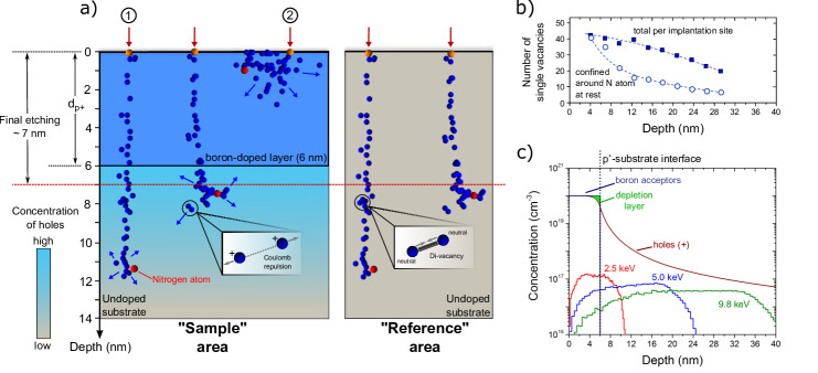
The kinetics of low energy (keV) ion implantation is dominated by energy loss through nuclear interactions between the implanted ion and the host latticeToyli et al. (2010). As a consequence, implantation-induced vacancies are distributed along the entire trajectory of the implanted ion with small deviations due to different contributions of ion channeling. This is in contrast to what has been observed for higher implantation energy (MeV), where electronic energy loss dominatesFairchild et al. (2008). We start by investigating the distribution of vacancies at individual implantation sites by Molecular Dynamics (MD) simulations. Individual nitrogen implantation events are simulated for a kinetic energy of keV in a -oriented diamond lattice (see Supplementary Information (SI) for further details). Implantation trajectories of nitrogen ions in diamond with identical implantation energies, but different ion implantation depths, are shown in figure 1a. Implantation sites labeled as and represent cases of pronounced contribution and absence of ion channeling, respectively. As seen in the two cases, the spatial distribution of the as-implanted vacancies is strongly influenced by ion channeling.
The number of vacancies created per implanted ion shows similar values when integrated over the whole implantation path, as shown in figure 1b. Nonetheless, the size of the resulting defect-cluster in a nanometer region surrounding the nitrogen atom at the end of the trajectory reduces with the implantation depth. This results in smaller numbers of vacancies in the immediate vicinity around the nitrogen atom at larger depths. Figure 1b shows a quantitative comparison of the number of vacancies confined around the nitrogen atom as a function of implantation depth. Low implantation energies lead to typical distances between single vacancies below nm, corresponding to local concentrations of cm-3. In contrast, ultra-pure diamond substrates with cm-3 concentration of nitrogen impuritiesYamamoto et al. (2013); de Oliveira et al. (2016) result in concentrations of free electrons of approximately cm-3 at high temperatures. Under these conditions, single vacancies are mainly in the neutral charge state, such that vacancy recombination results in the formation of V2 complexes with higher probability than the formation of a single NV center within individual defect-clustersDeák et al. (2014).
We further investigate the dynamics of vacancy diffusion by kinetic Monte Carlo (KMC) simulations at a temperature of C using the defect-cluster sizes simulated by MD as input. Our results indicate that approximately of all single vacancies within individual defect-clusters are expected to build V2 complexes or higher-order vacancy chains (see SI). A nanometer-volume surrounding individual NV centers is calculated to host up to V2 complexes after low energy nitrogen implantation and thermal annealing. The exact configuration of V2 spins depends however on the depth of individual NV centers (i.e. ion channeling contribution). These complexes are known to be thermally stableYamamoto et al. (2013) and are electron paramagnetic with a spin S Twitchen et al. (1999). In fact, numerical evaluation of the interaction Hamiltonian representing NV-V2 dipolar interactions shows that the presence of such a number of V2 electron spins in the vicinity of an NV center can be a dominating source of spin decoherence even in the close vicinity to the diamond surface, reducing times to a few µsHanson et al. (2008). These vacancy complexes are hence predicated as the major cause of spin decoherence and low formation yield of defect centers by nitrogen implantation. A method to suppress the formation of such defects during thermal annealing is thus a key step towards improving the quantum properties of spin defects.
I.2 The p+-i junction structure
One way to suppress vacancy recombination is to charge single vacancies in the defect-clusters during thermal annealing. In this case, Coulomb repulsion for near-neighbor charged vacancies is on the order of eV and hence greatly reduces the formation probability of V2 or higher order vacancy complexes. To implement this concept, we propose a planar all-diamond structure comprising a thin diamond layer with high concentration of boron acceptors (Ncm-3) epitaxially grown on a ultra-pure diamond substrate with a low concentration of donors (Ncm-3), as sketched in figure 1a. At thermodynamic equilibrium, positive charge carriers (holes) diffuse from the boron-doped layer into the substrate, resulting in the formation of a space charge dipole at the interface, identical to a planar p-n junction in semiconductors. The interface between the boron-doped layer and the substrate presents a step-like change in the concentration of acceptors with NA/ND ratio above , generating a nanometer depletion zone in the boron-doped layer. As a result, the near-interface region of the substrate is positively charged by the free carriers.
The depth profile of holes is shown in figure 1c, extracted from a D finite elements modeling (see Methods). In the figure, the corresponding depletion layer is represented by the green-marked area. The space charge profile extends to depths of above nm in the substrate, even for a small thickness of the boron-doped layer of nm. A suitable implantation energy of nitrogen thus localizes NV centers in this space charge layer, as seen in figure 1c. At a high concentration of holes in the substrate (Fermi level close to the valence band maximum), single vacancies are expected to be in the charge state during thermal annealingBernholc et al. (1988). As a final step of sample preparation, the surface is etched for nm to remove the boron-doped layer and leave a pristine and oxygen-terminated surfaceFávaro de Oliveira et al. (2015). A reference area (no boron-doped layer, see figure 1a, right) is fabricated on the same diamond to exclude any substrate-related effects such as variation in the intrinsic concentration of impurities in our experiments.
I.3 Formation yield of NV centers
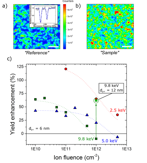
Figure 2 a and b present examples of confocal microscopy scans from the reference and p+-i junction (hereinafter referred to as “sample”) areas, respectively. The sample area shows a higher yield in comparison to the reference area for all three implantation energies, where an increase of approximately is observed, as seen in figure 2c. This supports the assumption that positively-charged vacancies localized within the space charge layer lead to enhanced self-diffusionBernholc et al. (1988) and an increased number of single vacancies available for the formation of NV centers. The observed enhancement also suggests a preferential path for the formation of NV centers: the implanted nitrogen atom is located in a split-interstitial site surrounded by single vacancies that occupy the nearest neighbor sitesSchwartz et al. (2012); Silverman et al. (2016). MD simulations further reveal that as-implanted nitrogen atoms in diamond occupy interstitial rather than substitutional positions ( and calculated probabilities, respectively)Antonov et al. (2014). Our results indicate that the recombination rate of a single vacancy and an interstitial nitrogen atom, followed by trapping a second vacancy located in the second-neighbor lattice position to form a stable NV center is enhanced by vacancies being positively charged. Electrostatic repulsion between vacancies should thus not only prevent the formation of vacancy complexes, but also facilitate the interstitial nitrogen atom (not charged) to occupy the nearest vacancy position.
From our results, we observe that the yield enhancement decreases with increasing nitrogen ion fluence for all implantation energies, as seen in figure 2c. This is due to the resulting charge compensation of holes induced by implantation-induced defects (e.g. charge traps and donor impurities). As shown in figure 2c, the ion fluence at which the enhancement is reduced to zero (“critical ion fluence”) shifts towards lower ion fluences for higher implantation energies. Since higher energies lead to a shift in the profile of implantation-induced defects towards the substrate region - as seen from the atomic profiles in figure 1c - we conclude that the charge compensation occurs in the substrate area. This is further supported by numerical simulations of the p+-i structure in the presence of compensating donors with different doping profiles (see SI). Moreover, in the case of our structure, charge compensation of acceptor impurities directly in the boron-doped layer, as previously discussed in Ref. Kalish et al. (1997), would result in the opposite behavior regarding the critical ion fluence vs. implantation energy.
In addition, the enhanced formation yield is still observed for the ion implantation with keV of energy and cm-2 ion fluence in the case of a second diamond fabricated with a thicker (nm) boron-doped layer (final etching of nm; see the highlighted square in figure 2c and SI). For this diamond, ion implantation with the same energy leads to a lower concentration of implantation-induced compensating defects in the substrate area, thus shifting the critical ion fluence towards higher values. This further supports that the charge compensation occurs in the substrate area rather in the boron-doped layer, as previously discussed. Importantly, the results obtained by the two different diamonds confirm indirectly the presence of holes in the substrate area of the fabricated structures.
I.4 Spin properties of NV centers
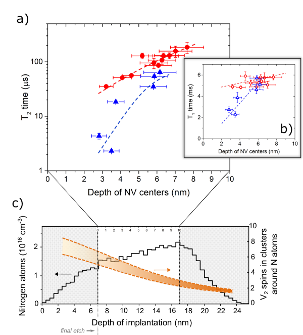
To address the impact of the surrounding implantation-induced defects, we use the NV centers themselves as sensors to probe the local environment. Comparing the sample and reference areas provides the opportunity to estimate directly the spin performance by using the p+-i junction structure. The experiments were carried out on defects created with keV of implantation energy and cm-2 ion fluence, owing to the possibility to sample implantation sites with different contributions of ion channeling. The spin coherence (Hahn-echo) and relaxation times (figures 3a and b, respectively) were measured for several NV centers at both regions. The depth of each NV center was measured independently (see Methods). As seen in figure 3a, times up to µs are observed for NV centers confined within nm of depth at the sample area.
By comparing NV centers with similar depths from the sample with the reference area, a tenfold improvement is seen for times for depths nm in the sample area. Remarkably, times measured from NV centers in the reference area approach the values of those from the sample area with increasing depth (see figure 3a). This behavior is attributed to the depth distribution of V2 spins, which are the dominant noise source for NV centers at depths nm in the reference region - as explained below. Nitrogen atoms implanted with keV of energy are expected to be distributed as shown by the atomic profile in figure 3c by CTRIMPosselt and Biersack (1992). In addition, the number of V2 complexes surrounding NV centers within individual defect-clusters is expected to be in the range given by the orange-dashed lines in figure 3c. These values were obtained by kinetic Monte Carlo simulation using the MD simulation results as input. As apparent from the figure, the number of V2 complexes per defect-cluster is reduced by a factor of three within nm of depth of NV centers (see upper scale limited by black-dashed vertical lines in figure 3c). In fact, for depths nm the number of V2 spins in close vicinity of the NV centers becomes negligible. For this depth range the magnetic noise from surface spins dominates the observed decoherence rate. Since the surface conditions are the same, similar values of are expected in the sample and reference areas, as indeed seen in our experiments (figure 3a).
However, NV centers located at depths nm are surrounded by V2 electron spins (figure 3c). A comparison between the depth-dependencies seen in figures 3a and c indicates that the additional noise contribution in the reference area arises mainly from the larger number of V2 electron spins in the vicinity of NV centers. Furthermore, a similar behavior is observed for the measured times, shown in figure 3b. The achieved values of ms are significantly longer than those typically observed for near-surface NV centersStaudacher et al. (2012); Ohashi et al. (2013); Rosskopf et al. (2014), thus assuring the pristine quality of the processed diamond. Both and values and depth dependencies further support the assumption that our method suppresses the formation of V2 complexes within individual defect-clusters.
I.5 Noise spectroscopy
To further analyze the magnetic noise affecting the NV centers at both the sample and reference areas, noise spectroscopy is utilizedMüller et al. (2010). Dynamic decoupling sequences with associated, characteristic spectral filter functionsCywiński et al. (2008); Álvarez and Suter (2011) are used to sample the magnetic noise sensed by NV centers (same from figure 3a and b) in different frequency ranges. Coherence decays were measured using the Carr-Purcell-Meiboom-Gill sequence (CPMG) with different numbers (N) of -pulses and spectral decomposition techniqueBar-Gill et al. (2012); Romach et al. (2015) was used to extract the corresponding noise spectra .
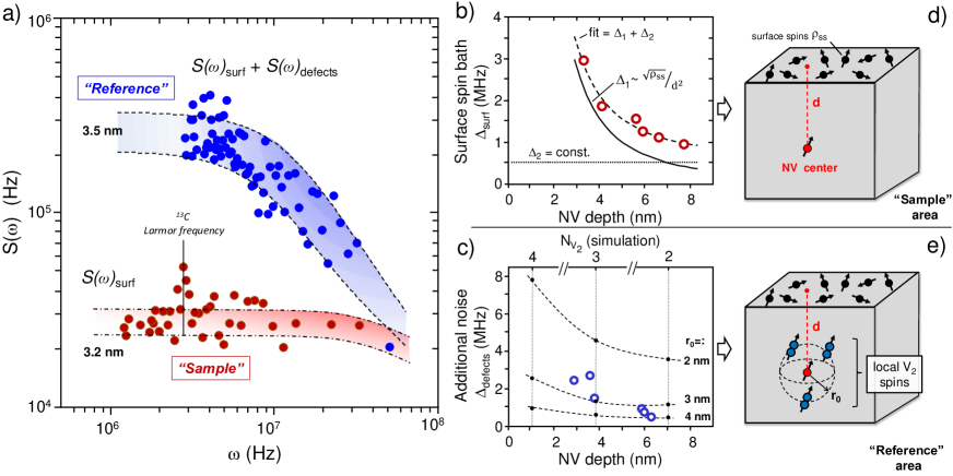
Figure 4a shows the resulting noise spectra corresponding to two NV centers located at the two areas with similar depths (nm) extracted from CPMG- decoherence decays. Single Lorentzian functions are used to fit the noise spectra extracted from NV centers in the sample areaBar-Gill et al. (2012); Romach et al. (2015). Figure 4b shows the related coupling strengths versus the depth of NV centers. The model used to fit the experimental data (dashed line) comprises two coupling strength contributions, and . The first corresponds to the surface spin bath, with a depth dependencyRosskopf et al. (2014) (solid line). The second is a contribution with constant amplitude (well below the amplitude related to surface spins), which represents the coupling to residual paramagnetic spins in the diamond lattice such as P centers and 13C nuclear spins.
Using this approach, a density of surface spins spins/cm2 is estimated, which is in good agreement with previous experimentsRosskopf et al. (2014). The derived value of is precisely in the range of the spatial density of electronic states for oxygen-terminated diamond surfaces. Such states are responsible for the band bending at the bare diamond surface and junction barriers of corresponding Schottky diode structuresMaier et al. (2001). Furthermore, noise spectra from NV centers in the sample area yield typical values of correlation times in the range of ns. For the mentioned density , the average distance of near-neighbor surface spins is approximately nm, corresponding to a mutual coupling of MHz (see SI). Hence, flip-flops among near-neighbor surface spins can lead to fluctuating magnetic noise at the NV center location with correlation times in the range of ns. Therefore, our experimental correlation times can be attributed mostly to spin-spin interactions between the near-surface NV center and the surrounding surface spin bath.
As mentioned, the surfaces of both sample and reference areas were treated identically, such that the two areas have identical surface spin bath characteristics. For this reason, we use a double-Lorentzian function to fit the noise spectra related to the reference region. This comprises the described fixed and an additional noise contributions, as depicted in figure 4a. For each depth of NV centers the parameters for the were set fixed according to the experimental data in figure 4b. In this way, we extract independently the coupling strengths and correlation times related to the additional noise source, which is responsible for the faster decoherence decay of near-surface NV centers in the reference area seen in figure 3a.
For the additional noise contribution, the extracted correlation times are in the range of ns. The coupling strengths versus the depth of NV centers are shown in figure 4c by blues circles. These values are in good agreement with numerical calculations (see SI) modeling the interaction of a few V2 spins with an NV center within individual defect-clusters. The calculated coupling strengths are given by black dots in figure 4c related to different numbers of V2 spins (, gray-doted vertical lines) distributed on a model sphere of radius r0 around a central NV center, as sketched in figure 4e. The corresponding number of V2 spins extracted from the experimental results shows that approximately of all single vacancies within individual defect-clusters build V2 complexes upon thermal annealing in the reference region, in agreement with the previously outlined MD/KMC simulation values in figure 3c. Importantly, this noise signature of V2 spins is only present in the reference region.
II Conclusion
The discussed experimental and numerical modeling results in a consistent picture of the formation dynamics of NV centers by low energy nitrogen implantation. They show that charging of single vacancies within defect-clusters is an effective method to suppress implantation-induced paramagnetic defects that degrade the spin performance of near-surface NV centers. This aspect is of particular interest since it can be extended to the broader field of ion implantation in semiconductor materials. Often, structural defects significantly deteriorate the optical, spin and charge transport properties, especially in the vicinity to surfaces and interfacesWolf et al. (2001). For diamond, we identify the formation of V2 complexes as a potential dominant source of spin decoherence, whereas for other materials different structural defects may account for spin decoherence. In all cases, there is a critical threshold for the size of defect-clusters which may not be eliminated by thermal annealingNastasi and Mayer (2006). As a result, charging of implantation-induced damage may be an universal tool towards better quantum properties of implanted spin defects. In addition, the presented results bring new insights in the dynamic mechanisms of self-diffusion and defect formation at single implantation sites, which enables new methods to further improve the engineering of spin defects. For instance, co-implantation of multiple atoms and moleculesJakobi et al. (2016) or implantation into more complex heterostructures combining strain engineeringGolter et al. (2016) with the presented structure might allow the fabrication of complex defect arrays. Extending the coherence times of near-surfaces spins and increasing the formation yield are decisive steps towards more sensitive nanoscale quantum sensing and coupling of single spins to e.g. superconducting resonators.
III Methods
III.1 Numerical simulations
Molecular Dynamics simulations were used to investigate the implantation of nitrogen atoms into the diamond lattice. The atomic interactions are represented by a combination of a bond-ordered Tersoff and a two-body Ziegler-Biersack-Littmark (for small atomic separation) potentials. The implanted atom is placed at a distance from the diamond surface beyond the Tersoff potential action range, with a kinetic energy of keV at nominally zero-angle (z-axis). Furthermore, several events of implantation were simulated separately for different x-y positions of the nitrogen atom in order to investigate the ion channeling effect.
The annealing process was simulated by means of kinetic Monte Carlo based on a model of hopping frequency of defects at a temperature of C. It includes the most important loss mechanisms for vacancies such as migration to the surface, recombination with interstitials and the formation of di-vacancies or higher-order vacancy complexes. The initial distribution of vacancies and nitrogen atom after implantation are taken from the results of Molecular Dynamics simulations.
The decoherence caused by di-vacancies on the electronic spin of single NV centers is estimated by numerical calculations. We model NV2 di-vacancies surrounding a central NV center with varying distance-radius r0. The di-vacancy electron spins (I ) are coupled to each other and to the central NV center electron spin (S) via magnetic dipole-dipole interaction. The corresponding equations are solved numerically to obtain the Hahn echo and CPMG-N decoherence decays, and corresponding noise coupling strength from the central NV center electron spin.
The -D depth profile of charge carriers presented in figure 1c was taken from a -D simulation of the thermodynamics equilibrium of the described planar p+-i junction structure by means of finite elements method (SILVACO softwarehttp://www.silvaco.com/ (2000)). Standard diamond parameters were used such as carrier concentration and mobility and the simulation mesh was optimized taking into account the relevant length scales. The simulated profile exhibits a quadratic-hyperbolical depth dependency of the concentration in the form , where is the characteristic Debye length related to the given boron doping in the p+ layer. The charge contribution of the ionized nitrogen donors in this sub-surface region of the substrate can be neglected since .
Further details about the described simulation methods can be found in the SI.
III.2 Boron-doped diamond growth and creation of NV centers
The heavily boron-doped diamond layers for the p+-i junction structures were overgrown by microwave plasma chemical vapor deposition in an ASTEX reactor on the surface of -oriented single-crystal electronic grade diamond substrates (<ppb nitrogen and boron, 13C - Element Six). The as-polished surfaces had prior to growth a root mean square (RMS) roughness of less than nm (measured by atomic force microscopy). The boron doping was realized in situ by introducing a solid boron rod in the plasma. Such a solid-state doping method enables the diamond overgrowth with a very sharp doping profile, approaching cm-3/nm. The used process parameters are described elsewhereAleksov et al. (2003). Importantly, due to absence of impurity diffusion in the diamond lattice, these layers remained stable at the used annealing conditions.
NV centers were created by implanting 15N+ ions with energies of , and keV by means of a focused ion beam in a home-built setup. The diamonds were annealed at C under high vacuum (mbar) for approximately two hours. The reference area and final etching steps were performed using oxygen inductively coupled plasma. This process enables nanometer-precise etching rate and was demonstrated to yield a pristine, oxygen-terminated surface while still preserving the optical and spin properties of NV centers located at a few nanometers of depthFávaro de Oliveira et al. (2015).
III.3 Depth calibration
The depth of individual NV centers at both the sample and reference areas were calibrated by means of spin relaxation techniqueSteinert et al. (2013). Reference values of were measured for the oxygen-terminated surface. Afterwards, a film (µm in thickness) containing Gd3+ ions at a nominal concentration of M was spin-coated on the diamond surface and times were measured to extract the gadolinium-induced spin relaxation. The depth was estimated using the model previously described in Ref. Steinert et al. (2013).
III.4 Spin properties of NV centers
For all spin measurements, a magnetic field of mT was applied along one of the possible orientations of NV centers. times were measured using a Hahn-echo sequence and the transverse relaxation times in the rotating frame () were measured using a CPMG dynamic decoupling sequence with N -pulses. These were fitted using:
where the first exponential term represents the main decoherence decay envelope with corresponding / time (), and the second sum term represents the electron spin echo envelope modulation (ESEEM) due to 13C spins in the diamond latticeOfori-Okai et al. (2012). is the number of revivals, is the corresponding periodicity, and is the initial fast coherence decay related to the ESEEM. measurements were fitted using a single exponential in the form .
III.5 Noise spectra
The decoherence decays () measured using CPMG pulse sequence were used to extract the noise spectra from individual NV centers. Noise spectral decomposition based on the filter function () arising from the used pulse sequenceBar-Gill et al. (2012); Cywiński et al. (2008) was used to deconvolve the noise spectra following:
The noise spectra presented are fitted according to:
where represents a single- or double-Lorentzian fit, respectively, is the noise coupling strength and is the correlation time between the NV center and the spin bath.
IV acknowledgments
The authors acknowledge the financial support from SFB/TR as well as the Volkswagen Foundation and the Max Planck Society. D. Antonov acknowledges the financial support by the DFG via the SBF . F. Fávaro de Oliveira acknowledges CNPq for the financial support through the project No. 204246/2013-0. We thank P. Deák for fruitful discussions.
V Author contributions
A.D designed the concept idea; F.F.O and A.D performed the experiments and data analysis, assisted by S.A.M.; D.A. and T.H. performed the MD and KMC simulations; Y.W. performed the numerical calculations of the NV-V2 interaction Hamiltonian; A.P. assisted with the boron-doped diamond growth; P.N., A.D. and J.W. supervised the work; all authors contributed to the manuscript writing.
VI Competing financial interests
The authors declare no competing financial interests.
References
- Morton et al. (2011) J. J. L. Morton, D. R. McCamey, M. A. Eriksson, and S. A. Lyon, Nature 479, 345 (2011).
- Steger et al. (2012) M. Steger, K. Saeedi, M. L. W. Thewalt, J. J. L. Morton, H. Riemann, N. V. Abrosimov, P. Becker, and H.-J. Pohl, Science 336, 1280 (2012).
- Dehollain et al. (2016) J. P. Dehollain, S. Simmons, J. T. Muhonen, R. Kalra, A. Laucht, F. Hudson, K. M. Itoh, D. N. Jamieson, J. C. McCallum, A. S. Dzurak, and A. Morello, Nat Nano 11, 242 (2016).
- Togan et al. (2010) E. Togan, Y. Chu, A. S. Trifonov, L. Jiang, J. Maze, L. Childress, M. V. G. Dutt, A. S. Sørensen, P. R. Hemmer, A. S. Zibrov, and M. D. Lukin, Nature 466, 730 (2010).
- Dutt et al. (2007) M. V. G. Dutt, L. Childress, L. Jiang, E. Togan, J. Maze, F. Jelezko, A. S. Zibrov, P. R. Hemmer, and M. D. Lukin, Science 316, 1312 (2007).
- Neumann et al. (2008) P. Neumann, N. Mizuochi, F. Rempp, P. Hemmer, H. Watanabe, S. Yamasaki, V. Jacques, T. Gaebel, F. Jelezko, and J. Wrachtrup, Science 320, 1326 (2008).
- Waldherr et al. (2014) G. Waldherr, Y. Wang, S. Zaiser, M. Jamali, T. Schulte-Herbrüggen, H. Abe, T. Ohshima, J. Isoya, J. F. Du, P. Neumann, and J. Wrachtrup, Nature 506, 204 (2014), letter.
- Mamin et al. (2013) H. J. Mamin, M. Kim, M. H. Sherwood, C. T. Rettner, K. Ohno, D. D. Awschalom, and D. Rugar, Science 339, 557 (2013).
- Staudacher et al. (2013) T. Staudacher, F. Shi, S. Pezzagna, J. Meijer, J. Du, C. A. Meriles, F. Reinhard, and J. Wrachtrup, Science 339, 561 (2013).
- Häberle et al. (2015) T. Häberle, D. Schmid-Lorch, F. Reinhard, and J. Wrachtrup, Nat Nano 10, 125 (2015).
- Shi et al. (2015) F. Shi, Q. Zhang, P. Wang, H. Sun, J. Wang, X. Rong, M. Chen, C. Ju, F. Reinhard, H. Chen, J. Wrachtrup, J. Wang, and J. Du, Science 347, 1135 (2015).
- Doherty et al. (2013) M. W. Doherty, N. B. Manson, P. Delaney, F. Jelezko, J. Wrachtrup, and L. C. L. Hollenberg, Physics Reports 528, 1 (2013).
- Momenzadeh et al. (2015) S. A. Momenzadeh, R. J. Stöhr, F. F. de Oliveira, A. Brunner, A. Denisenko, S. Yang, F. Reinhard, and J. Wrachtrup, Nano Letters 15, 165 (2015).
- Jamali et al. (2014) M. Jamali, I. Gerhardt, M. Rezai, K. Frenner, H. Fedder, and J. Wrachtrup, Review of Scientific Instruments 85 (2014), 10.1063/1.4902818.
- Li et al. (2015) L. Li, E. H. Chen, J. Zheng, S. L. Mouradian, F. Dolde, T. Schröder, S. Karaveli, M. L. Markham, D. J. Twitchen, and D. Englund, Nano Letters 15, 1493 (2015).
- Ovartchaiyapong et al. (2014) P. Ovartchaiyapong, K. W. Lee, B. A. Myers, and A. C. B. Jayich, Nat. Commun. 5, 4429 (2014).
- Ali Momenzadeh et al. (2016) S. Ali Momenzadeh, F. F. de Oliveira, P. Neumann, D. D. Bhaktavatsala Rao, A. Denisenko, M. Amjadi, Z. Chu, S. Yang, N. B. Manson, M. W. Doherty, and J. Wrachtrup, Phys. Rev. Applied 6, 024026 (2016).
- Balasubramanian et al. (2009) G. Balasubramanian, P. Neumann, D. Twitchen, M. Markham, R. Kolesov, N. Mizuochi, J. Isoya, J. Achard, J. Beck, J. Tissler, V. Jacques, P. R. Hemmer, F. Jelezko, and J. Wrachtrup, Nature Materials 8, 383 (2009).
- DiVincenzo (2000) D. P. DiVincenzo, Fortschritte der Physik 48, 771 (2000).
- Pezzagna et al. (2010a) S. Pezzagna, D. Wildanger, P. Mazarov, A. D. Wieck, Y. Sarov, I. Rangelow, B. Naydenov, F. Jelezko, S. W. Hell, and J. Meijer, Small 6, 2117 (2010a).
- Pezzagna et al. (2010b) S. Pezzagna, B. Naydenov, F. Jelezko, J. Wrachtrup, and J. Meijer, New Journal of Physics 12, 065017 (2010b).
- Ofori-Okai et al. (2012) B. K. Ofori-Okai, S. Pezzagna, K. Chang, M. Loretz, R. Schirhagl, Y. Tao, B. A. Moores, K. Groot-Berning, J. Meijer, and C. L. Degen, Phys. Rev. B 86, 081406 (2012).
- Yamamoto et al. (2013) T. Yamamoto, T. Umeda, K. Watanabe, S. Onoda, M. L. Markham, D. J. Twitchen, B. Naydenov, L. P. McGuinness, T. Teraji, S. Koizumi, F. Dolde, H. Fedder, J. Honert, J. Wrachtrup, T. Ohshima, F. Jelezko, and J. Isoya, Phys. Rev. B 88, 075206 (2013).
- Dolde et al. (2013) F. Dolde, I. Jakobi, B. Naydenov, N. Zhao, S. Pezzagna, C. Trautmann, J. Meijer, P. Neumann, F. Jelezko, and J. Wrachtrup, Nat Phys 9, 139 (2013).
- Silverman et al. (2016) A. Silverman, J. Adler, and R. Kalish, Communications in Computational Physics 19, 380 (2016).
- Toyli et al. (2010) D. M. Toyli, C. D. Weis, G. D. Fuchs, T. Schenkel, and D. D. Awschalom, Nano Letters 10, 3168 (2010).
- Fairchild et al. (2008) B. A. Fairchild, P. Olivero, S. Rubanov, A. D. Greentree, F. Waldermann, R. A. Taylor, I. Walmsley, J. M. Smith, S. Huntington, B. C. Gibson, D. N. Jamieson, and S. Prawer, Advanced Materials 20, 4793 (2008).
- de Oliveira et al. (2016) F. F. de Oliveira, S. A. Momenzadeh, D. Antonov, J. Scharpf, C. Osterkamp, B. Naydenov, F. Jelezko, A. Denisenko, and J. Wrachtrup, Nano Letters 16, 2228 (2016).
- Deák et al. (2014) P. Deák, B. Aradi, M. Kaviani, T. Frauenheim, and A. Gali, Phys. Rev. B 89, 075203 (2014).
- Twitchen et al. (1999) D. J. Twitchen, M. E. Newton, J. M. Baker, T. R. Anthony, and W. F. Banholzer, Phys. Rev. B 59, 12900 (1999).
- Hanson et al. (2008) R. Hanson, V. V. Dobrovitski, A. E. Feiguin, O. Gywat, and D. D. Awschalom, Science 320, 352 (2008).
- Bernholc et al. (1988) J. Bernholc, A. Antonelli, T. M. Del Sole, Y. Bar-Yam, and S. T. Pantelides, Phys. Rev. Lett. 61, 2689 (1988).
- Fávaro de Oliveira et al. (2015) F. Fávaro de Oliveira, S. A. Momenzadeh, Y. Wang, M. Konuma, M. Markham, A. M. Edmonds, A. Denisenko, and J. Wrachtrup, Applied Physics Letters 107, 073107 (2015).
- Antonov et al. (2014) D. Antonov, T. Häußermann, A. Aird, J. Roth, H.-R. Trebin, C. Müller, L. McGuinness, F. Jelezko, T. Yamamoto, J. Isoya, S. Pezzagna, J. Meijer, and J. Wrachtrup, Applied Physics Letters 104, 012105 (2014), 10.1063/1.4860997.
- Schwartz et al. (2012) J. Schwartz, S. Aloni, D. F. Ogletree, and T. Schenkel, New Journal of Physics 14, 043024 (2012).
- Kalish et al. (1997) R. Kalish, C. Uzan-Saguy, B. Philosoph, V. Richter, and S. Prawer, Applied Physics Letters 70, 999 (1997).
- Rosskopf et al. (2014) T. Rosskopf, A. Dussaux, K. Ohashi, M. Loretz, R. Schirhagl, H. Watanabe, S. Shikata, K. M. Itoh, and C. L. Degen, Phys. Rev. Lett. 112, 147602 (2014).
- Posselt and Biersack (1992) M. Posselt and J. P. Biersack, Nucl. Instr. Meth. Phys. Res. Sec. B 64, 706 (1992).
- Staudacher et al. (2012) T. Staudacher, F. Ziem, L. Häussler, R. Stöhr, S. Steinert, F. Reinhard, J. Scharpf, A. Denisenko, and J. Wrachtrup, Applied Physics Letters 101, 212401 (2012), 10.1063/1.4767144.
- Ohashi et al. (2013) K. Ohashi, T. Rosskopf, H. Watanabe, M. Loretz, Y. Tao, R. Hauert, S. Tomizawa, T. Ishikawa, J. Ishi-Hayase, S. Shikata, C. L. Degen, and K. M. Itoh, Nano Letters 13, 4733 (2013).
- Müller et al. (2010) G. M. Müller, M. Oestreich, M. Römer, and J. Hübner, Physica E: Low-dimensional Systems and Nanostructures 43, 569 (2010).
- Cywiński et al. (2008) L. Cywiński, R. M. Lutchyn, C. P. Nave, and S. Das Sarma, Phys. Rev. B 77, 174509 (2008).
- Álvarez and Suter (2011) G. A. Álvarez and D. Suter, Phys. Rev. Lett. 107, 230501 (2011).
- Bar-Gill et al. (2012) N. Bar-Gill, L. Pham, C. Belthangady, D. Le Sage, P. Cappellaro, J. Maze, M. Lukin, A. Yacoby, and R. Walsworth, Nat. Commun. 3, 858 (2012).
- Romach et al. (2015) Y. Romach, C. Müller, T. Unden, L. J. Rogers, T. Isoda, K. M. Itoh, M. Markham, A. Stacey, J. Meijer, S. Pezzagna, B. Naydenov, L. P. McGuinness, N. Bar-Gill, and F. Jelezko, Phys. Rev. Lett. 114, 017601 (2015).
- Maier et al. (2001) F. Maier, J. Ristein, and L. Ley, Phys. Rev. B 64, 165411 (2001).
- Wolf et al. (2001) S. A. Wolf, D. D. Awschalom, R. A. Buhrman, J. M. Daughton, S. von Molnár, M. L. Roukes, A. Y. Chtchelkanova, and D. M. Treger, Science 294, 1488 (2001).
- Nastasi and Mayer (2006) M. Nastasi and J. W. Mayer, “Ion implantation and synthesis of materials,” (Springer-Verlag Berlin Heidelberg, 2006).
- Jakobi et al. (2016) I. Jakobi, S. A. Momenzadeh, F. F. de Oliveira, J. Michl, F. Ziem, M. Schreck, P. Neumann, A. Denisenko, and J. Wrachtrup, Journal of Physics: Conference Series 752, 012001 (2016).
- Golter et al. (2016) D. A. Golter, T. Oo, M. Amezcua, K. A. Stewart, and H. Wang, Phys. Rev. Lett. 116, 143602 (2016).
- http://www.silvaco.com/ (2000) http://www.silvaco.com/, “Silvaco,” (2000).
- Aleksov et al. (2003) A. Aleksov, A. Denisenko, M. Kunze, A. Vescan, A. Bergmaier, G. Dollinger, W. Ebert, and E. Kohn, Semiconductor Science and Technology 18, S59 (2003).
- Steinert et al. (2013) S. Steinert, F. Ziem, L. T. Hall, A. Zappe, M. Schweikert, N. Götz, A. Aird, G. Balasubramanian, L. Hollenberg, and J. Wrachtrup, Nat. Commun. 4, 1607 (2013).