Electronic Properties, Screening and Efficient Carrier Transport in NaSbS2
Abstract
NaSbS2 is a semiconductor that was recently shown to have remarkable efficacy as a solar absorber indicating efficient charge collection even in defected material. We report first principles calculations of properties that show (1) an indirect gap only slightly smaller than the direct gap, which may impede recombination of photoexcited carriers, (2) highly anisotropic electronic and optical properties reflecting a layered crystal structure, (3) a pushed up valence band maximum due to repulsion from the Sb states and (4) cross-gap hybridization between the S derived valence bands and the Sb states. This latter feature leads to enhanced Born effective charges that can provide local screening and therefore defect tolerance. These features are discussed in relation to the performance of the compound as a semiconductor with efficient charge collection.
I Introduction
NaSbS2 is a little studied semiconductor that was recently shown to be remarkably effective as a solar absorber material, Rahayu et al. (2016) and has also been mentioned as a potential thermoelectric material based on computational screening. Bhattacharya et al. (2016) Remarkably, an efficiency of 3.18% was obtained in the first report using NaSbS2 nanparticles in a dye sensitized solar cell. Rahayu et al. (2016) This is comparable to the efficiency of early cells of similar type made using organometallic halide perovskites. Kojima et al. (2009) Those materials have since proven to be a revolutionary advance in photovoltaics, but suffer from issues with long term stability and the fact that they contain Pb, which is undesirable. Lee et al. (2012); Giustino and Snaith (2016) NaSbS2 contains only environmentally friendly low cost elements, and this very promising early experimental result, and the theoretical results below suggest that it may as well represent a revolutionary new material for solar photovoltaic applications.
From a valence point of view one might regard the stoichiometry as derived from PbS by splitting of the divalent Pb site into monovalent Na and trivalent Sb. In this way one might anticipate that NaSbS2 would be a semiconductor and that the band gap may be higher than that of PbS if normal trends are followed due to the splitting of the cation site. However, at ambient temperature the crystal structure deviates strongly the rocksalt structure of PbS, as discussed below. More significantly, the presence of Na suggests a propensity for defects, e.g. Na off-stoichiometry. Good charge collection requires a high carrier drift length, which typically occurs in high quality defect free material, and so the high performance of NaSbS2 as a solar absorber is surprising. However, several soft lattice solar materials have been discovered, most notably CH3NH3PbI3, Lee et al. (2012) where defects do not seem to play the same detrimental role as in more traditional materials such as CdTe. Stranks et al. (2013) Here we report first principles calculations aimed at understanding the properties of this compound, especially in relation to its use as a solar absorber.
II Structure and Methods
The present calculations were performed within density functional theory (DFT). The electronic structure and optical properties were calculated using the general potential linearized augmented planewave (LAPW) method, Singh and Nordstrom (2006) as implemented in the WIEN2k code. Blaha et al. (2001) The total energy calculations and relaxation of the atomic coordinates was done using the Perdew, Burke and Ernzerhof (PBE) generalized gradient approximation (GGA). Perdew et al. (1996) For this, relativity was treated at a scalar relativistic level for the valence states. The core states were treated relativistically. LAPW sphere radii of =2.2 bohr were used for all elements, along with a planewave sector basis cutoff determined by, =9 (here is the radius of the smallest LAPW sphere, i.e. 2.2 bohr, and is the planewave cutoff). Local orbitals were added to the basis for the S , Na and , and Sb semicore states.
Spin-orbit was included for the electronic and optical properties. The band gap is important for these, and accordingly these calculations were done using the modified Becke-Johnson (mBJ) potential of Tran and Blaha. Tran and Blaha (2009) This functional gives band gaps in good accord with experiment for a wide variety of simple semiconductors and insulators and also appears to give reliable band shapes and optical properties, although at least in certain semiconductors the band masses are more similar to those obtained in standard density functional calculations than those from many body calculations. Tran and Blaha (2009); Koller et al. (2011); Singh (2010a); Kim et al. (2010); Singh (2010b) Calculation of the transport function for conductivity was done using the BoltzTraP code. Madsen and Singh (2006) Optical properties were calculated based on electric dipole transitions in the independent particle approximation as implemented in the WIEN2k code. The Born effective charges and the dielectric tensor were calculated using the density functional perturbation theory (DFPT) with the PBE functional as implemented in the VASP code Kresse and Furthmüller (1996) (note that calculation of the dielectric tensor cannot be done with the mBJ potential, since it is not an energy functional and therefore cannot be used to evaluate lattice response).
The structure of NaSbS2 has been refined into two different monoclinic groups, (# 15) Olivier-Fourcade et al. (1978) and (# 12). Volk and Schafer (1978) In addition there is a report of a triclinic structure (# 2). Kanischeva et al. (1979) These are all centrosymmetric structures. The deviation from a cubic structure was discussed in terms of lone pair activity of Sb. Olivier-Fourcade et al. (1978)
III Results and Discussion
We did calculations for the three reported structures, in each case using the lattice parameters from the diffraction experiments, and then relaxing the atomic positions subject to the spacegroup symmetry. We find that the energy for the structure is 0.127 eV per formula unit (f.u.) above the energy of the structure. The structure is 0.005 eV/f.u. higher than the structure.
We did further calculations to address the issue of the ground state. Specifically, we did full relaxations, including both lattice parameters, angles and internal coordinates. For this purpose we used the VASP code with three different density functionals, specifically the local density approximation (LDA), the PBE GGA Perdew et al. (1996) and the PBEsol GGA. Perdew et al. (2009) We further did full relaxations of both the and the structures using VASP with LDA, PBE, and PBEsol Perdew et al. (2009) functionals. These functionals differ in equilibrium volumes for solids. Generally, at increased volume lattices tend to distort more strongly, as was noted in the case of PbTiO3, an oxide ferroelectric with a ground state particularly sensitive to volume. Wu and Cohen (2006) We find that the LDA underestimates the unit cell volume of NaSbS2, yielding 175 Å3, in comparison with the experimental volume of 192 Å3 at 300 K. The PBE functional yields 197 Å3, while PBEsol yields 184 Å3. The LDA predicts a monoclinic ground state, while the fully relaxed triclinic structure is 2 meV/atom lower in energy for both PBE and PBEsol. Considering the very small energy, and the limitations of DFT calculations we conclude that the ground state is monoclinic or possibly with an extremely small triclinic distortion from this monoclinic structure. The other monoclinic structure, , is, however, clearly not a feasible structure.
We calculated properties for both the and structures, but find very little difference. For example, the band gap for the triclinic structure is 1.21 eV compared to 1.22 eV for the monoclinic. This is not surprising since the two structures are very similar, though not identical. Internal coordinates for the two structures are given in Tables 1 and 2. As seen, the bond valences Brown (1985) are close to their nominal values indicative of an ionic structure, Na+Sb3+S, although the Sb value of 2.85 is slightly smaller perhaps indicative of some degree of covalency.
| b.v. | ||||
|---|---|---|---|---|
| Na | 0.0000 | 0.7500 | 0.1340 | 1.06 |
| Sb | 0.0000 | 0.7500 | 0.6051 | 2.85 |
| S | 0.2239 | 0.7606 | 0.4088 | 2.02 |
| b.v. | ||||
|---|---|---|---|---|
| Na | 0.3658 | 0.6332 | 0.2501 | 1.06 |
| Sb | 0.8947 | 0.1049 | 0.2499 | 2.84 |
| S | 0.1330 | 0.3156 | 0.7393 | 2.02 |
| S | 0.3154 | 0.1320 | 0.2390 | 2.02 |
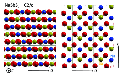
In the following, we discuss properties of the monoclinic structure for simplicity. The structure is depicted in Fig. 1. As seen, it is a layered structure, with two layers per unit cell. The layers have composition NaSbS2, with all atoms coplanar in the monoclinic structure and very nearly coplanar in the triclinic structure. A single layer is depicted in the right panel of Fig. 1. The layers show distinct short bonds between Sb and two neighboring S in the same layer leading to apparent S-Sb-S units. These units would lead to a strong ferroelectricity in plane with polarization along the -direction, except that the two layers per cell have opposite orientation so that the polarizations of the individual sheets cancel. The formation of S-Sb-S units leads to a dimerization of the S in the layers. The near neighbor Sb-S distance is 2.486 Å, while the S-Sb-S angle is 98.6∘. The chains of S-Sb-S units run along the -direction. Thus the structure has anisotropic layers in the - plane. In the following discussion of optical and electronic properties we use a orthogonal coordinate system where is along the -axis, is along the -axis and is perpendicular to these. The tensor properties show an component due to the monoclinicity.
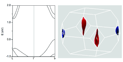
The band structure near the band edges is depicted in Fig. 2, which shows the band structure along lines where the band extrema occur and a isosurface visualization of the band edges. The valence band maximum (VBM) is on a zone face, as shown, at the point denoted “b”. The conduction band minimum (CBM) is near, but not at, another zone face (L). This indirect band gap has a value, =1.22 eV. The direct gap, is at “b”, and is only 0.02 eV (250 K) larger. This structure can provide a partial explanation for observed good collection of photoexcited carriers. Specifically, while the very small difference between and is insignificant from the point of view of obtaining good optical absorption for the solar spectrum, the indirect nature of the gap will impede recombination of photoexcited carriers that relax to the band edges. This effect will be stronger at room temperature if the difference between the direct and indirect gaps is a little larger, which is possible considering uncertainties in DFT calculations. We note that 0.02 eV is a small energy and so it will be of importance to verify whether the gap is indirect and if so the magnitude of the difference between the direct and indirect gaps by experiment.
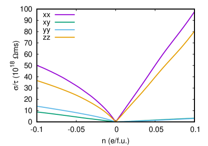
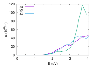
Fig. 3 shows the transport function as obtained from the electronic structure. As seen, the transport is highly two dimensional for both the conduction and valance bands, but is more so for the conduction bands. Transport in plane is also anisotropic, with better conduction along the (-direction) than along . This amounts to 35% for the valence bands and 20% for the conduction bands. Finally, if the effective scattering rates, , are similar for electrons and holes, the in-plane mobility will be higher for electrons than for holes.
The calculated optical absorption spectrum is given in Fig. 4. This spectrum was calculated in the independent particle approximation, i.e. neglecting excitonic effects. These are anticipated to be small due to the small band gap and resulting high electronic (clamped ion) dielectric constant. The spectrum is similar for both in plane polarizations but differs strongly for the yy component, which has electric field polarization perpendicular to the NaSbS2 sheets. Regardless of polarization, the absorption is relatively weak from the onset at the direct gap to 2.5 eV. This emphasizes the important role of good carrier transport to realize the reported efficacy of this material as a solar absorber. Rahayu et al. (2016)
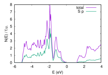
Fig. 5 shows the calculated electronic density of states along with the S contribution. The valence bands are derived from S states, so that the compound should be regarded as nominally ionic. The top of the valence band manifold also appears to be split off to higher energy. This type of splitting is seen in some other S compounds where it arises from repulsion between a lower lying metal state and the S states. Chen et al. (2009); Mitzi et al. (2011) The result is that the top of the valence band has antibonding metal - S character, and often more dispersive bands beneficial for transport.
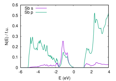
This antibonding mechanism is operative here. Fig. 6 shows and projections on the Sb LAPW spheres. As seen, there is Sb character at the top of the valence bands including at the VBM. The main Sb bands are at -9.5 to -7 eV relative to the VBM, and so the VBM has S - Sb antibonding character.
Besides this Sb character at the top of the valence bands, there is considerable Sb character in the valence bands. The Sb states are nominally unoccupied in this compound and form the main conduction bands. Thus this Sb contribution in the valence bands comes from cross-gap hybridization between the occupied S states and unoccupied Sb states. Such cross-gap hybridization is a characteristic of oxide ferroelectric materials where it leads to enhanced Born effective charges and thus ferroelectricity, Cohen (1992) and is also found in phase change materials. Mukhopadhyay et al. (2016) It is closely connected with the concept of lone pair driven distortions. Enhanced Born effective charges have also been associated with efficient carrier transport in a number of materials. Du and Singh (2010a, b); Fabini et al. (2016); Brandt et al. (2015); Lehner et al. (2015); Du (2014) The mechanism is enhanced local screening due to the high Born charge, which leads to defect tolerance in soft lattice materials. Du and Singh (2010a); Brandt et al. (2015)
The Born effective charges were obtained as = , where is the volume of the unit cell, is the total polarization in direction and is the displacement in direction . The calculated Born effective charges of monoclinic NaSbS2 are shown in Table 3. It can be seen that the maximum Born effective charges are 1.47 for Na, 4.69 for Sb and -3.08 for S, respectively. These are considerably larger than the corresponding nominal charges, consistent with the expectation from the electronic structure. The dielectric tensor contains both the electronic and ionic contributions as = + . The electronic part was obtained with ion-clamped using DFPT. Gajdoš et al. (2006); Baroni and Resta (1986) The ionic contribution was based on the interatomic force constants calculated using DFPT.Wu et al. (2005) For monoclinic NaSbS2, there are four non-zero components, as given in Table 4. The average value given by one third of the trace is 23.8. For comparison, ZnO, which is a good oxide semiconductor that has some defect tolerance at least for -type, Look (2001); McCluskey and Jokela (2009) has a dielectric constant of 9.3. Crisler et al. (1968)
| Na | 1.13 | -0.15 | 0.00 | -0.15 | 1.47 | 0.00 | 0.00 | 0.00 | 1.19 |
|---|---|---|---|---|---|---|---|---|---|
| Sb | 3.43 | 1.55 | 0.00 | 1.51 | 4.69 | 0.00 | 0.00 | 0.00 | 2.31 |
| S | -2.28 | -0.70 | 1.38 | -0.68 | -3.08 | 0.57 | 0.80 | 0.02 | -1.75 |
| 9.3 | 1.7 | 8.4 | 7.4 | |
| 10.4 | 13.0 | 32.7 | 3.3 | |
| 19.7 | 14.7 | 41.1 | 10.7 |
Therefore NaSbS2 has enhanced Born effective charges due to the cross gap hybridization, similar to several materials that have been found to have excellent charge collection in the context of radiation detection, e.g. TlBr, BiI3 and Tl6SeI4. Du and Singh (2010a, b); Biswas et al. (2012) This enhanced Born charge leads to an enhanced dielectric constant, which means enhanced screening. This provides an explanation of how a material that presumably contains high concentrations of point defects can nonetheless have efficient carrier collection in an optoelectronic application. In this regard, we note that SrTiO3, which is near a ferroelectric transition, and consequently has a very high dielectric constant at low temperature, also has an exceptional electron mobility that exceeds 30,000 cm2/Vs in high quality films. Son et al. (2010)
IV Summary and Conclusions
We report first principles calculations for NaSbS2. We find that the ground state structure is monoclinic 2/ or possibly triclinic with a very small triclinic distortion. We find highly anisotropic electronic and optical properties as may be expected based on the crystal structure. The results show a quasidirect band gap, with an indirect gap slightly lower than the direct gap, which may impede carrier recombination. The calculated value of the band gap using the mBJ potential is 1.22 eV. Importantly, the electronic structure shows a substantial cross gap hybridization between S and Sb states. This results in enhanced Born effective charges and a high dielectric constant. This high dielectric constant provides screening and defect tolerance for the carrier collection. Therefore it is likely that NaSbS2 can be a useful optoelectronic material, not only as a solar absorber, but also in applications requiring doping.
Acknowledgements.
This work was supported by the Department of Energy through the MAGICS Center, Award DE-SC0014607.References
- Rahayu et al. (2016) S. U. Rahayu, C. L. Chou, N. Suriawong, B. A. Aragaw, S. B. Shi, and M. W. Lee, “Sodium antimony sulfide (NaSbS2): turning an unexpected impurity into a promising, environmentally friendly novel solar absorber material,” APL Mater. 4, 116103 (2016).
- Bhattacharya et al. (2016) S. Bhattacharya, R. Chmielowski, G. Dennler, and G. K. H. Madsen, “Novel ternary sulfide thermoelectric materials from high throughput transport and defect calculations,” J. Mater. Chem. A 4, 11086–11093 (2016).
- Kojima et al. (2009) A. Kojima, K. Teshima, Y. Shirai, and T. Miyasaka, “Organometal halide perovskites as visible-light sensitizers for photovoltaic cells,” J. Am. Chem. Soc. 131, 6050–6051 (2009).
- Lee et al. (2012) M. M. Lee, J. Teuscher, T. Miyasaka, T. N. Murakami, and H. J. Snaith, “Efficient hybrid solar cells based on meso-structured organometal halide perovskites,” Science 338, 643–647 (2012).
- Giustino and Snaith (2016) F. Giustino and H. J. Snaith, “Toward lead-free perovskite solar cells,” ACS Energy Lett. 1, 1233–1240 (2016).
- Stranks et al. (2013) S. D. Stranks, G. E. Eperon, G. Grancini, C. Menelaou, M. J. P. Alcocer, T. Leijtens, L. M. Herz, A. Petrozza, and H. J. Snaith, “Electron-hole diffusion lengths exceeding 1 micrometer in an organometal trihalide perovskite absorber,” Science 342, 341–344 (2013).
- Singh and Nordstrom (2006) D. J. Singh and L. Nordstrom, Planewaves Pseudopotentials and the LAPW Method, 2nd Edition (Springer, Berlin, 2006).
- Blaha et al. (2001) P. Blaha, K. Schwarz, G. Madsen, D. Kvasnicka, and J. Luitz, WIEN2k, An Augmented Plane Wave + Local Orbitals Program for Calculating Crystal Properties (K. Schwarz, Tech. Univ. Wien, Austria, 2001).
- Perdew et al. (1996) J. P. Perdew, K. Burke, and M. Ernzerhof, “Generalized gradient approximation made simple,” Phys. Rev. Lett. 77, 3865–3868 (1996).
- Tran and Blaha (2009) F. Tran and P. Blaha, “Accurate band gaps of semiconductors and insulators with a semilocal exchange-correlation potential,” Phys. Rev. Lett. 102, 226401 (2009).
- Koller et al. (2011) D. Koller, F. Tran, and P. Blaha, “Merits and limits of the modified Becke-Johnson exchange potential,” Phys. Rev. B 83, 195134 (2011).
- Singh (2010a) D. J. Singh, “Electronic structure calculations with the Tran-Blaha modified Becke-Johnson density functional,” Phys. Rev. B 82, 205102 (2010a).
- Kim et al. (2010) Y. S. Kim, M. Marsman, G. Kresse, F. Tran, and P. Blaha, “Towards efficient band structure and effective mass calculations for III-V direct band gap semiconductors,” Phys. Rev. B 82, 205212 (2010).
- Singh (2010b) D. J. Singh, “Structure and optical properties of high light output halide scintillators,” Phys. Rev. B 82, 155145 (2010b).
- Madsen and Singh (2006) G. K. H. Madsen and D. J. Singh, “BoltzTraP a code for calculating band-structure dependent quantities,” Comput. Phys. Commun. 175, 67–71 (2006).
- Kresse and Furthmüller (1996) G. Kresse and J. Furthmüller, “Efficient iterative schemes for ab initio total-energy calculations using a plane-wave basis set,” Phys. Rev. B 54, 11169 (1996).
- Olivier-Fourcade et al. (1978) J. Olivier-Fourcade, E. Philippot, and M. Maurin, “Structure des composes NaSbS2 et NaSbS2 . etude de l’influence de la paire electronique e de i’antimonine III dans ia transition NaSbS2 - NaSbS2 ,” Z. Anorg. Allg. Chem. 446, 159–168 (1978).
- Volk and Schafer (1978) K. Volk and H. Schafer, “Die kristallstruktur von b-NaSbS2,” Z. Naturforsch. 33b, 827–828 (1978).
- Kanischeva et al. (1979) A. S. Kanischeva, V. G. Kuznetsov, and V. N. Batog, “Crystal structure of a-NaSbS2,” J. Struct. Chem. 20, 122–125 (1979).
- Perdew et al. (2009) J. P. Perdew, A. Ruzsinszky, G. I. Csonka, O. A. Vydrov, G. E. Scuseria, L. A. Constantin, X. Zhou, and K. Burke, “Restoring the density-gradient expansion for exchange in solids and surfaces,” Phys. Rev. Lett. 102, 039902 (2009).
- Wu and Cohen (2006) Z. Wu and R. E. Cohen, “More accurate generalized gradient approximation for solids,” Phys. Rev. B 73, 235116 (2006).
- Brown (1985) I. D. Brown, “Bond-valence parameters obtained from a systematic analysis of the inorganic crystal structure database,” Acta Cryst. B 41, 244–247 (1985).
- Chen et al. (2009) S. Chen, X. G. Gong, A. Walsh, and S. H. Wei, “Crystal and electronic band structure of Cu2ZnSnX4 (X=S and Se) photovoltaic absorbers: first principles insights,” Appl. Phys. Lett. 94, 041903 (2009).
- Mitzi et al. (2011) D. B. Mitzi, O. Gunawan, T. K. Totorov, and S. Guha, “The path towards a high-performance solution-processed kesterite solar cell,” Solar Energy Materials and Solar Cells 95, 1421–1436 (2011).
- Cohen (1992) R. E. Cohen, “Origin of ferroelectricity in perovskite oxides,” Nature 358, 136–138 (1992).
- Mukhopadhyay et al. (2016) S. Mukhopadhyay, J. Sun, A. Subedi, T. Siegrist, and D. J. Singh, “Competing covalent and ionic bonding in Ge-Sb-Te phase change materials,” Sci. Rep. 6, 25981 (2016).
- Du and Singh (2010a) M. H. Du and D. J. Singh, “Enhanced born charge and proximity to ferroelectricity in thallium halides,” Phys. Rev. B 81, 144114 (2010a).
- Du and Singh (2010b) M. H. Du and D. J. Singh, “Enhanced born charges in III-VI, IV-VII2 and V-VII3 compounds,” Phys. Rev. B 82, 045203 (2010b).
- Fabini et al. (2016) D. H. Fabini, T. Hogan, H. A. Evans, C. C. Stoumpos, M. G. Kanatzidis, and R. Seshadri, “Dielectric and thermodynamic signatures of low-temperature glassy dynamics in the hybrid perovskites CH3NH3PbI3 and HC(NH2)(2)PbI2,” J. Phys. Chem. Lett. 7, 376–381 (2016).
- Brandt et al. (2015) R. E. Brandt, V. Stevanovic, D. S. Ginley, and T. Buonassisi, “Identifying defect-tolerant semiconductors with high minority-carrier lifetimes: beyond hybrid lead halide perovskites,” MRS Commun. 5, 265–275 (2015).
- Lehner et al. (2015) A. J. Lehner, D. H. Fabini, H. A. Evans, C. A. Hebert, S. R. Smock, J. Hu, H. B. Wang, J. W. Zwanziger, M. L. Chabinyc, and R. Seshadri, “Crystal and electronic structures of complex bismuth iodides A(3)Bi(2)I(9) (A = K, Rb, Cs) related to perovskite: Aiding the rational design of photovoltaics,” Chem. Mater. 27, 7137–7148 (2015).
- Du (2014) M. H. Du, “Efficient carrier transport in halide perovskites: theoretical perspectives,” J. Mater. Chem. A 2, 9091–9098 (2014).
- Gajdoš et al. (2006) M. Gajdoš, K. Hummer, G. Kresse, J. Furthmüller, and F. Bechstedt, “Linear optical properties in the projector-augmented wave methodology,” Phys. Rev. B 73, 045112 (2006).
- Baroni and Resta (1986) S. Baroni and R. Resta, “Ab initio calculation of the macroscopic dielectric constant in silicon,” Phys. Rev. B 33, 7017 (1986).
- Wu et al. (2005) X. Wu, D. Vanderbilt, and D. R. Hamann, “Systematic treatment of displacements, strains, and electric fields in density-functional perturbation theory,” Phys. Rev. B 72, 035105 (2005).
- Look (2001) D. C. Look, “Recent advances in ZnO materials and devices,” Mat. Sci. Eng. B 80, 383 (2001).
- McCluskey and Jokela (2009) M. D. McCluskey and S. J. Jokela, “Defects in ZnO,” J. Appl. Phys. 106, 071101 (2009).
- Crisler et al. (1968) D. F. Crisler, J. J. Cupal, and A.R. Moore, “Dielectric, piezoelectric and electromechanical coupling constants of zinc oxide crystals,” Proc. IEEE 56, 225–226 (1968).
- Biswas et al. (2012) K. Biswas, M. H. Du, and D. J. Singh, “Electronic structure and defect properties of Tl6SeI4: density functional calculations,” Phys. Rev. B 86, 144108 (2012).
- Son et al. (2010) J. Son, P. Moetakef, B. Jalan, O. Bierwagen, N. J. Wright, R. Engel-Herbert, and S. Stemmer, “Epitaxial SrTiO3 films with electron mobilities exceeding 30,000 cm2 V-1s-1,” Nature Mater. 9, 482 (2010).