Proximity induced spin-valley polarization in silicene/germanene on F-doped WS2
Abstract
Silicene and germanene are key materials for the field of valleytronics. However, interaction with the substrate, which is necessary to support the electronically active medium, becomes a major obstacle. In the present work, we propose a substrate (F-doped WS2) that avoids detrimental effects and at the same time induces the required valley polarization, so that no further steps are needed for this purpose. The behavior is explained by proximity effects on silicene/germanene, as demonstrated by first-principles calculations. Broken inversion symmetry due to the presence of WS2 opens a substantial band gap in silicene/germanene. F doping of WS2 results in spin polarization, which, in conjunction with proximity-enhanced spin orbit coupling, creates sizable spin-valley polarization.
I Introduction
Silicene and germanene are topological insulators with nontrivial band gaps of 2 meV and 24 meV, respectively, induced by spin orbit coupling (SOC) Fv . The band gap can be controlled electrically by applying a gate voltage in the out-of-plane direction tune . It is anticipated that both materials host quantum spin Hall qshe , quantum anomalous Hall qahe , and valley polarized quantum anomalous Hall vpqahe phases. Silicene has been prepared on various substrates ex1 ; ex2 ; si_zrb2 ; a1 , while it is questionable whether it can exist in freestanding form (which also applies to germanene). This is the reason why various theoretical results on the interaction with possible substrates are found in the literature, including the insulator -BN hbn1 , the semiconductor GaAs sigaas , and the metals Ca simetal , Ag ag , and Ir ir . While on metallic substrates the Dirac behavior of silicene typically is not maintained subst1 ; subst2 , transition metal dichalcogenides are characterized by a weak interaction simos2 . From a different perspective, the latter class of materials is receiving great interest in recent days due to the fact that it realizes band gaps in a technologically attractive range tmdc . Transition metal dichalcogenides also have proven to be suitable hosts for graphene grap1 ; grap2 and it has been demonstrated that the SOC of graphene can be enhanced by three orders of magnitude to about 17 meV on WS2 due to proximity effects soprox .
Valleytronics is emerging as a new and exciting area of research, aiming to exploit the valley degree of freedom in Dirac materials valley1 ; valley2 . An essential prerequisite of valleytronics, of course, is the availability of materials with valley polarization, i.e., the energetical degeneracy of the valleys at the high symmetry K and K′ points of the hexagonal Brillouin zone must be lifted. While this is difficult to realize in graphene, the stronger SOC and buckled lattice of silicene/germanene provide an avenue to access and control the valley degree of freedom tronics . Spin and valley polarization can be achieved by means of doping and decoration with certain or transition metals tm3d ; tm4d as well as by an external electric field ef ; qahe ; vpqahe . However, interaction with the substrate is typically detrimental, because the electronic states are perturbed subst3 . Besides the need to reduce the interaction with the substrate, it would be a great advantage if the substrate itself can be used to induce the required valley polarization, in order to reduce the complexity of the system. In this context, we show in the present work that proximity effects between silicene/germanene and WS2 can be utilized to obtain a suitable platform to explore spin and valley physics. We first discuss the band characteristics and spin splitting in silicene/germanene induced by the strong SOC in WS2 and afterwards demonstrate that the spin polarization in F-doped WS2 generates spin-valley polarization.
II Computational method
We use the Vienna Ab-initio Simulation Package to perform first-principles calculations based on density functional theory vasp . The exchange correlation potential is described in the generalized gradient approximation, using the Perdew-Burke-Ernzerhof scheme, and the plane wave cutoff energy is set to a sufficiently large value of 475 eV. Moreover, the SOC is taken into account in all calculations and the van der Waals interaction is incorporated using the DFT-D3 method dftd3 . The optimized lattice constants of silicene, germanene, and WS2 are 3.86 Å, 4.05 Å, and 3.18 Å. In order to reduce the lattice mismatch to 2.9% and 1.9%, respectively, a supercells of silicene and germanene are placed on top of a supercell of WS2. Vacuum slabs of 15 Å thickness are used to obtain two-dimensional models. For the Brillouin zone integration, Monkhorst-Pack and k-meshes are employed in the structure relaxations and band structure calculations, respectively. We achieve in each case at least an energy convergence of eV and an atomic force convergence of eV/Å.
III Results and Discussion
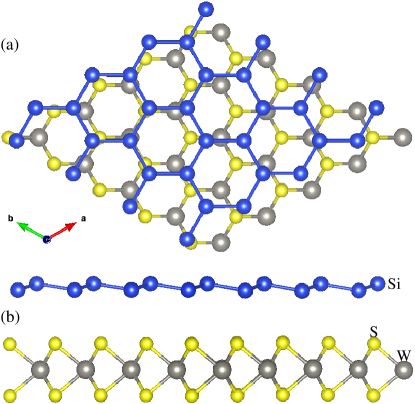
The optimized crystal structure of silicene on top of monolayer WS2 is illustrated in Fig. 1. A corresponding figure for germanene looks very similar and therefore is not shown. For different stackings of silicene/germanene on top of WS2 (different lateral shifts) we obtain very small (few meV) total energy differences, showing that the materials can easily slide on each other. The distance between the two component materials turns out to be 3.13 Å in the case of silicene and 2.90 Å in the case of germanene. While the buckling of silicene is hardly affected by the interaction with WS2 (0.46 Å), it is slightly enhanced to 0.74 Å for germanene (0.65 Å in the freestanding case). The smaller interlayer distance and the enhancement of the buckling demonstrate that WS2 interacts more with germanene than with silicene, though the coupling is still weak. In order to quantify the interaction, we calculate the binding energy , given by the total energies of the combined system, freestanding silicene/germanene, and freestanding monolayer WS2. Furthermore, is the number of Si/Ge atoms. We obtain values of meV and meV for silicene and germanene, respectively, confirming our conclusion that the interaction is stronger in the latter case.
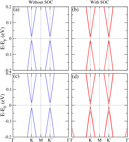
The electronic band structures in Fig. 2 show that both silicene and germanene on WS2 maintain a linear dispersion of the bands in the vicinity of the Fermi energy. This is the case both when the SOC is neglected and when it is taken into account. Without SOC we obtain band gaps of 29 meV and 38 meV, see Fig. 2(a/c), for silicene and germanene on WS2, respectively, which is comparable to the thermal energy at room temperature. The reason for the opening of a band gap is the broken inversion symmetry in the presence of WS2. SOC lifts the spin degeneracy at the K and K′ points and results in spin splittings of 8 meV and 32 meV in the valence band of silicene and germanene, respectively, and 3 meV and 19 meV in the conduction band, see Fig. 2(b/d). The effect of the SOC is enhanced in the presence of WS2 as a consequence of tiny hybridization between the Si/Ge and W orbitals. WS2 indeed is characterized by very strong SOC, as reflected by spin splittings of 431 meV (valence band) and 29 meV (conduction band) in a freestanding monolayer epl . The enhancement mechanism by proximity SOC is similar to the case of graphene on transition metal dichalcogenides origin2 , but due to the buckling of silicene/germanene the magnitude of spin splitting here is different in the valence and conduction bands. As a consequence of the lifted spin degeneracy, we obtain reduced band gaps of 23 meV and 14 meV for silicene and germanene on WS2, respectively.
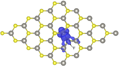
In the following we will argue that silicene/germanene on F-doped WS2 develops energetically inequivalent band edges at the K and K′ points, i.e., spin-valley polarization. The advantage of doping the substrate instead of the electronically active material (the material giving rise to the states close to the Fermi energy) is that impurity scattering is avoided. Specifically, we replace one S atom in the supercell of WS2 with an F atom, corresponding to a doping concentration of 2%, in order to simulate the dilute doping limit. An earlier study has shown that substitutional F doping at the S site is possible in MoS2 doping_prb . We calculate the binding energies and obtain values of 4.3 eV for X = F and 6.1 eV for X = S, where is the energy of a relaxed WS2 monolayer with one S vacancy, is the energy of an X atom, and is the energy of a relaxed WS2 monolayer with one S atom replaced by an X atom. Since the binding energies of F and S are similar, it is likely that substitutional F doping at the S site is also possible in WS2. Experimental support for this conclusion comes from the realization of P doping in MoS2 and WSe2 b1 ; b2 and Cl doping in MoS2 and WS2 b3 . By comparing spin degenerate and polarized calculations for the doped supercell, we obtain an energy gain of 134 meV in the spin polarized case and a total magnetic moment of 1 . Next to the F atom the charge transfer from the three neighbouring W atoms is reduced from two electrons to one electron (F-1 state instead of S-2 state). The remaining electron is located on one of the three W atoms and gives rise to the spatial distribution of spin density shown in Fig. 3. We obtain a small F magnetic moment of 0.05 , which is also reflected by Fig. 3.
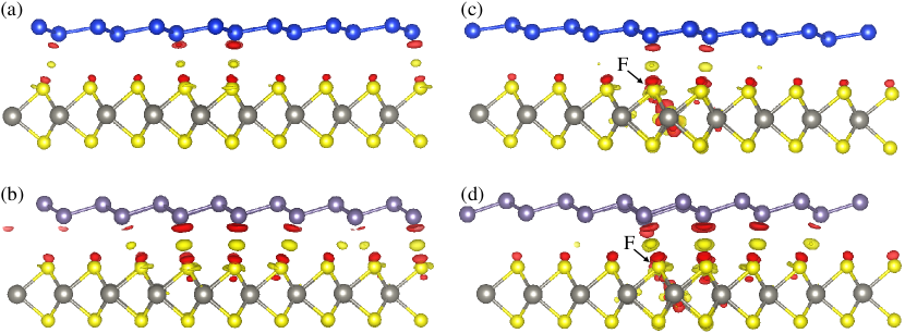
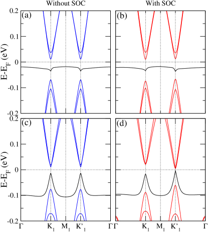
We obtain for silicene and germanene on top of F-doped WS2 smaller distances between the component materials, 3.06 Å and 2.79 Å, respectively, as compared to the case of pristine WS2. This fact can be attributed to the additional magnetic coupling. A comparison of the interaction in the cases of pristine and F-doped WS2 is given in Fig. 4 in terms of charge density difference plots. While the charge redistribution in the van der Waals gap is only slightly modified after F doping, compare the top to the bottom row of Fig. 4, the dopant atom is strongly affected, supporting the idea of magnetic coupling. We obtain still a total magnetic moment of 1 , carried largely by one W atom. This atom realizes a larger distance (2.70 Å) to the F atom than the other two neighbouring W atoms (2.30 Å), very similar to the situation without silicene/germanene. In addition, the F magnetic moment is reduced to . The band structure of silicene/germanene shows significant alterations in contact with F-doped WS2, see Fig. 5. Without SOC, the spin splitting in the valence band is enhanced to 36/91 meV and that in the conduction band to 25/9 meV. This fact is expected to simply reduce the band gaps, however, we observe in both cases the creation of an in-gap band just below the Fermi energy. Analysis of the orbital character of this band shows that it arises almost purely from the F impurity.
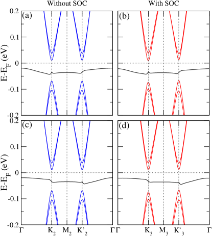
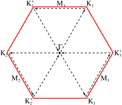
Broken time-reversal symmetry due to the spin polarization in F-doped WS2 induces spin-valley polarization in silicene/germanene when the SOC is taken into account, see Fig. 5(b/d). Specifically, the spin splitting in the valence/conduction band (not counting the F impurity band) is smaller/larger at the K than at the K′ point. For silicene we obtain values of 28 meV and 40 meV for the valence band and 27 and 24 meV for the conduction band, respectively. More importantly, valley polarization of 7 meV is created in the silicene valence band and one of 2 meV in the conduction band. For germanene these effects are enhanced, with spin splittings of 74 meV and 111 meV (valence band) as well as 4 meV and 5 meV (conduction band) at the K and K′ points, respectively. The valley polarization here amounts to 28 meV and 16 meV for the germanene valence and conduction bands, respectively, which opens a route to spin-valley polarization even at room temperature. In order to demonstrate that the K and K′ valleys are virtually not affected by the symmetry breaking in F-doped WS2, as they belong almost purely to silicene/germanene, we show in Fig. 6 for the silicene system the band structures of the 2 K and 2 K′ points not covered by Fig. 5(a/b). We observe no lifting of the valley degeneracy in the case without SOC and exactly the same valley structure as before in the case with SOC. We also have checked that the spin hybridization at the valleys is negligible. Moreover, while the F impurity band is located next to the Fermi energy, the F states are spatially separated from the Si/Ge states and therefore do not limit exploitation of the spin-valley polarization.
In conclusion, we have demonstrated that silicene and germanene in proximity to monolayer WS2 develop sizeable band gaps (due to inversion symmetry breaking) and spin splittings (due to proximity SOC). F doping of WS2 results in spin polarization with a total magnetic moment of 1 , since the charge transfer from the three neighbouring W atoms is reduced. The remaining spin polarized electron is largely located on one W atom. Our main finding is that F-doped WS2 makes it possible to achieve substantial spin-valley polarization in silicene and germanene. In contrast to silicene, germanene even can enable valleytronics devices operating at ambient conditions.
Acknowledgements.
The research reported in this publication was supported by funding from King Abdullah University of Science and Technology (KAUST).References
- (1) S. Cahangirov, M. Topsakal, E. Aktürk, H. Sahin, and S. Ciraci, Phys. Rev. Lett. 102, 236804 (2009).
- (2) Z. Ni, Q. Liu, K. Tang, J. Zheng, J. Zhou, R. Zin, Z. Gao, D. Yu, and J. Lu, Nano Lett. 12, 113 (2012).
- (3) C. C. Liu, W. Feng, and Y. Yao, Phys. Rev. Lett. 107, 076802 (2011).
- (4) M. Ezawa, Phys. Rev. Lett. 109, 055502 (2012).
- (5) H. Pan, Z. Li, C. C. Liu, G. Zhu, Z. Qiao, and Y. Yao, Phys. Rev. Lett. 112, 106802 (2014).
- (6) P. Vogt, P. D. Padova, C. Quaresima, J. Avila, E. Frantzeskakis, M. C. Asensio, A. Resta, B. Ealet, and G. Le Lay, Phys. Rev. Lett. 108, 155501 (2012).
- (7) L. Chen, C. C. Liu, B. Feng, X. He, P. Cheng, Z. Ding, S. Meng, Y. Yao, and K. Wu, Phys. Rev. Lett. 109, 056804 (2012).
- (8) A. Fleurence, R. Friedlein, T. Ozaki, H. Kawai, Y. Wang, and Y. Y. Takamura, Phys. Rev. Lett. 108, 245501 (2012).
- (9) L. Tao, E. Cinquanta, D. Chiappe, C. Grazianetti, M. Fanciulli, M. Dubey, A. Molle, and D. Akinwande, Nat. Nanotechnol. 10, 227 (2015).
- (10) Z. X. Guo, S. Furuya, J. Iwata, and A. Oshiyama, Phys. Rev. B 87, 235435 (2013).
- (11) A. Bhattacharya, S. Bhattacharya, and G. P. Das, Appl. Phys. Lett. 103, 123113 (2013).
- (12) P. Pflugradt, L. Matthes, and F. Bechstedt, New J. Phys. 16, 075004 (2014).
- (13) Z. X. Guo, S. Furuya, J. I. Iwata, and A. Oshiyama, J. Phys. Soc. Jpn. 82, 063714 (2013).
- (14) L. Meng, Y. Wang, L. Zhang, S. Du, R. Wu, L. Li, Y. Zhang, G. Li, H. Zhou, W. A. Hofer, and H. J. Gao, Nano Lett. 13, 685 (2013).
- (15) S. Cahangirov, M. Audiffred, P. Tang, A. Iacomino, W. Duan, G. Merino, and A. Rubio, Phys. Rev. B 88, 035432 (2013).
- (16) C. L. Lin, R. Arafune, K. Kawahara, M. Kanno, N. Tsukahara, E. Minamitani, Y. Kim, M. Kawai, and N. Takagi, Phys. Rev. Lett. 110, 076801 (2013).
- (17) N. Gao, J. C. Li, and Z. Jiang, Phys. Chem. Chem. Phys. 16, 11673 (2014).
- (18) Q. H. Wang, K. K. Zadeh, A. Kis, J. N. Coleman, and M. S. Strano, Nat. Nanotech. 7, 699 (2012).
- (19) C. P. Lu, G. Li, K. Watanabe, T. Taniguchi, and E. Y. Andrei, Phys. Rev. Lett. 113, 156804 (2014).
- (20) T. Georgiou, R. Jalil, B. D. Belle, L. Britnell, R. V. Gorbachev, S. V. Morozov, Y. J. Kim, A. Gholinia, S. J. Haigh, O. Makarovsky, L. Eaves, L. A. Ponomarenko, A. K. Geim, K. S. Novoselov, and A. Mishchenko, Nat. Nanotech. 8, 100 (2013).
- (21) A. Avsar, J. Y. Tan, T. Taychatanapat, J. Balakrishnan, G. K. W. Koon, Y. Yeo, J. Lahiri, A. Carvalho, A. S. Rodin, E. C. T. O’Farrel, G. Eda, A. H. Castro Neto, and B. Özyilmaz, Nat. Commun. 5, 4875 (2014).
- (22) A. Rycerz, J. Tworzydlo, and C. W. J. Beenakker, Nat. Phys. 3, 172 (2007).
- (23) D. Xiao, W. Yao, and Q. Niu, Phys. Rev. Lett. 99, 236809 (2007).
- (24) M. Ezawa, Phys. Rev. B 87, 155415 (2013).
- (25) X. L. Zhang, L. F. Liu, and W. M. Liu, Sci. Rep. 3, 2908 (2013).
- (26) J. Zhang, B. Zhao, and Z. Yang, Phys. Rev. B 88, 165422 (2013).
- (27) W. F. Tsai, C. Y. Huang, T. R. Chang, H. Lin, H. T. Jeng, and A. Bansil, Nat. Commun. 4, 1500 (2013).
- (28) M. Satta, S. Colonna, R. Flammini, A. Cricenti, and F. Ronci, Phys. Rev. Lett. 115, 026102 (2015).
- (29) G. Kresse and D. Joubert, Phys. Rev. B: Condens. Matter 59, 1758 (1999).
- (30) S. Grimme, J. Antony, S. Ehrlich, and H. Krieg, J. Chem. Phys. 132, 154104 (2010).
- (31) Y. C. Cheng, Z. Y. Zhu, M. Tahir, and U. Schwingenschlögl, EPL 102, 57001 (2013).
- (32) M. Gmitra, D. Kochan, P. Högl, and J. Fabian, Phys. Rev. B 93, 155104 (2016).
- (33) K. Dolui, I. Rungger, C. D. Pemmaraju, and S. Sanvito, Phys. Rev. B 88, 075420 (2013).
- (34) E. Kim, C. Ko, K. Kim, Y. Chen, J. Shuh, S.-G. Ryu, K. Wu, X. Meng, A. Suslu, S. Tongay, J. Wu, and C. P. Grigoropoulos, Adv. Mater. 28, 341 (2016).
- (35) A. Nipane, D. Karmakar, N. Kaushik, S. Karande, and S. Lodha, ACS Nano 10, 2128 (2016).
- (36) L. Yang, K. Majumdar, H. Liu, Y. Du, H. Wu, M. Hatzistergos, P. Y. Hung, R. Tieckelmann, W. Tsai, C. Hobbs, and P. D. Ye, Nano Lett. 14, 6275 (2014).