Photoinduced valley polarized current of layered by electric tuning
Abstract
Photoinduced current of layered based transistor is studied from first principles. Under the illumination of circular polarized light, valley polarized current is generated which can be tuned by the gate voltage. For monolayer , the valley polarized spin up (down) electron current at () points is induced by the right (left) circular polarized light. The valley polarization is found to reach +1.0 (-1.0) for valley current that carried such a () index. For bilayer , the spin up (down) current can be induced at both and valleys by the right (left) circular light. In contrast to monolayer , the photoinduced valley polarization shows asymmetric behavior upon reversal of the gate voltage. Our results show that the valley polarization of photoinduced current can be modulated by the circular polarized light and the gate voltage. All the results can be well understood using a simple KP model.
pacs:
73.63.-b, 78.67.-n, 85.60.-qAs one of the most promising two-dimensional materials, graphene has shown exceptional physical, chemical, and optical properties.Singh ; Andrei ; Qiao ; Bao However, pristine graphene doesn’t have gap between valence band and conduction band which hampers its applications in semiconductor devices. Although layered transition-metal dichalcogenide (TMDC) has the similar hexagonal structure like graphene, it shows distinctly different properties from graphene.Radisavljevic ; novoselov ; CLee ; Tkorn Firstly, TMDC has strong spin-orbit coupling which is originated from the orbitals of the heavy metal atoms. This makes TMDC an exciting platform to explore spintronic applications.ZYZhu ; HMin ; YYao Secondly, monolayer TMDC, due to its inversion symmetry breaking, displays distinct physical properties from its bulk counterpart. TMDC crossovers from an indirect band gap semiconductor at bulk to a direct band gap semiconductor at monolayer.KFMak ; ASplendiani Most importantly, monolayer TMDC has six valleys at the corners of its hexagonal Brillouin zone, which can be classified into two inequivalent groups. Such valleys have large separations in momentum space which makes the valley index robust against small deformation of its lattice and low-energy scattering by long wavelength phonon. This means that the valley index can be used as a potential information carrier. The valley properties of graphene has been extensively studied theoretically.ARycerz ; Dxiao ; FZhang Recently, there has been a growing interest in the special spin and valley properties of layered TMDC both experimentally and theoretically.AMJones ; Dxiao2 Xiao et al Dxiao2 found that in monolayer TMDC, inversion symmetry breaking and spin orbit coupling (SOC) lead to coupled spin and valley physics. Monolayer TMDC has opposite spins at the two inequivalent points, making the optical transition rules between valence band and conduction band both spin-dependent and valley-dependent. Carriers with various combinations of valley and spin indices can be selectively excited by optical fields with different circular polarizations.WYao ; HYuan Circularly polarized luminescence has been observed in monolayer and bilayer under circularly optical pumping with different frequencies.Hzeng ; Swu This confirms the theoretical prediction that the circular polarization originates from the contrasting selection rules for optical transitions in different valleysWYao .
For the potential device application of layered TMDC, the key issue is to examine the performance of nanoelectronic devices such as transistors. Indeed, the properties of electron-hole transport and photovoltaic effect in gated Schottky junction were studied.MFontana The phototransistor based on monolayer exhibited good photoresponsivity and prompt photoswitching, and the mechanism of photoresponse was analyzed in the ultrathin field-effect transistors by scanning photoinduced current microscopy.OLopez ; RSsundaram ; ZYin ; CWu So far, most of the investigations concentrate on the I-V characteristics and less attention has been paid on the valley information. Since one of the major challenges in valleytronics is the generation of valley polarized current, it is important to study the valley polarized current through layered . In this letter, we investigate the properties of valley polarized current of layered phototransistor from first principles and analyze our results using KP model.
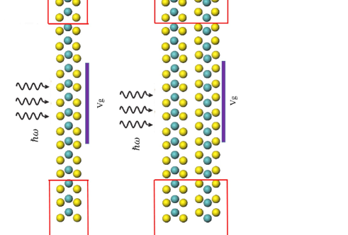
In this work, we calculate the photoinduced valley polarized current in monolayer and bilayer phototransistors. As shown in Fig.1, the phototransistor consists of two semi-infinite sheets of monolayer/bilayer as leads and a central scattering region. A vertical electric field E along direction is produced by applying the gate voltage at the bottom gate in the central scattering region. In the numerical calculation, the sizes of supercells used in our calculation are set to be 10.34 47.77 40.0 for monolayer and 10.34 47.77 55.0 for bilayer . The band gaps we get here are eV for monolayer and eV for bilayer , which are similar to those of reference Kadantsev, and reference QihangLiu, , although they are under estimated comparing to the experimental results of reference KFMak . We will focus on the transport along armchair direction when the circularly polarized light is shined on the central region. An external bias voltage V is applied across the central region in order to collect valley polarized photo current. The energy of incident light is assumed to be equal to the direct energy gap for monolayer and for bilayer , respectively.
To calculate the photoinduced current of such devices, we treat electron-photon coupling as a perturbation on the self consistent Hamiltonian of electronic degrees of freedom .RLake ; LEHenrickson ; JChen To obtain the nonequilibrium Hamiltonian of open structures, we employ the state-of-the-art first principles method based on the combination of density functional theory and the Keldysh nonequilibrium Green’s function formalism (NEGF-DFT).LKleinman The system nonequilibrium Hamiltonian is self-consistently determined through NEGF-DFT calculation which includes spin-orbital coupling (SOI), external bias voltage and gate voltage. Since the light consists of both electric and magnetic fields, the current density function theory (CDFT) may be more appropriate to describe the photocurrent.Vignale For small field strength as is the case in this paper, DFT may be a good approximation.
Our calculation was preformed using the first principles package NanoDCal.JTaylor ; Guohong Double- basis set was used to expand the wave functions and the exchange-correlation potential was treated at local spin density approximation (LSDA) level.JPPerdew ; Kubler ; Kubler2 ; Nordstrom The mesh cut-off energy was set to be 200 Ry and numerical tolerance of self-consistency was restricted to eV. To consider the -sampling, mesh in -space is used. After obtaining , we treated the electron-photon interaction by the first order Born approximation. Here, , where is the electromagnetic vector potential and the momentum of the electron. Detailed procedures of obtaining Green’s function have been discussed in reference Lzhang, .
The photoinduced valley and spin dependent current in the lead can be written asLzhang ; HHaug
| (1) |
Here, stands for the lead of source/drain. (corresponding to /) is the valley index and around or is calculated starting from the point of or , is the spin index. is the effective transmission coefficient of lead , and its expression is
| (2) |
where, is the Fermi distribution function of lead , is the linewidth function which reflects the coupling between lead and central scattering region, is the Green’s function including the contribution of voltage and photons.Lzhang
To describe the current response to the light, we examine the photoresponse, which is defined as
| (3) |
where is the current with valley index and spin index . is the photon flux defined as the number of photons per unit time per unit area.
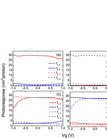
Figure 2 shows the valley and spin polarized photoresponse versus gate voltage under bias voltage 0.3 V. The solid red line, solid blue line, dashed red line, and dashed blue line correspond to photoresponse , , , and , respectively. From panel (a), we see that the component , is at least one order of magnitude larger than other three components, indicating that the right circular polarized light mainly excites the spin-up electrons at point from the valence band to the conduction band in monolayer . Similarly we conclude from figure 2(b) that the left circular polarized light mainly excites the spin-down electrons at point in monolayer . This phenomenon is due to the symmetry breaking in monolayer and can be explained by optical selection rule.Dxiao2 The situation is different for bilayer where the inversion symmetry is restored. In this case, the spin up components of photonresponse ( and ) are much larger than the other two components when light is shed (panel(c)), whereas the spin down components ( and ) dominate for light (panel(d)).
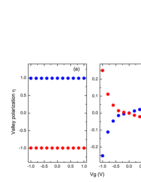
To characterize valley injection, we define valley polarization as
| (4) |
where . From the panel (a) of figure 3, we see that almost fully polarized valley current is generated using either or incident light. In addition, the valley polarizations remain constant in the whole range of gate voltages from -1.0 V to 1.0 V, suggesting that valley polarization of monolayer is robust against the gate voltage. In contrast, we find that the valley polarization is very sensitive to the gate voltage for bilayer . As shown in panel (b) of figure 3, the valley polarization changes from -0.25 to 0.05 in bilayer (blue dot line in panel (b)) in the gate voltage window V when light is shed. The valley polarization profile satisfies . Hence for bilayer , the valley polarization can be modulated by the circular polarized light as well as the gate voltage. We also find that the modulation effect of negative gate voltage is more significant than that of positive one. To explain all of these phenomena, we examine the following KP model.
Due to the inversion symmetry breaking and the presence of strong spin-orbit coupling in monolayer , spin and valley degrees of freedom couple to each together, i.e, () valley is occupied by the spin-up (down) electrons at the top of the valence band. The electron interband transition from the top of spin-split valence band to the bottom of the conduction band can be induced by the circular polarized light . If we define the coupling strength with optical fields as , we have the following coupling intensity for transitions near pointsDxiao2
| (5) |
where , , is the free electron mass, is the lattice constant, is the effective hopping integral, is the energy gap, is the valley index, 2 is the spin splitting at the top of valence band caused by SOC, and is for spin. To characterize the polarization of coupling, we define
| (6) |
Here, . Since is very small near or points, we have . This in turn gives from Eq. (6). The behavior of polarization of coupling intensity is almost the same as that of valley current polarization obtained from ab initio calculation shown in figure 3(a). This suggests that the polarization of valley current calculated from ab initio method is intimately related to the polarization of coupling from the KP model in monolayer .
The situation is more complicated in bilayer . In this paper, we consider AB stacked bilayer which maintains the inversion symmetry. To mimic the effect of the gate voltage in ab initio calculation, we introduce an electric field along direction in our KP model Hamiltonian. The KP model Hamiltonian for bilayer with perpendicular external electric field is expressed as follows:GZRui
| (7) |
where is the intralayer hopping constant, , is the magnitude of external electric field and is the distance between two monolayers. The external electric field will induce an energy shift of at upper layer and an energy shift at lower layer in the bilayer . Here all the parameters in Eq.(7) are taken from the reference GZRui, and the basis is {,,, }.
By diagonalizing Eq. (7), we obtain the eigenfunctions , , , and with near the top valence band as follows,
| (8) |
with
and
| (10) |
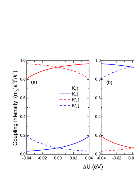
Under the illumination of circular polarized light, the coupling intensities are found to be
Figure 4 shows the coupling intensity versus the two layer potential energy difference in bilayer by KP model. The results are similar to those of figure 2 by the ab initio method. Our ab initio calculation shows that V gives rise a potential difference 0.04 V between the top and bottom layers in bilayer . Hence we plot the coupling intensity versus from V to V in figure 4 in order to compare with figure 2, where is from -1.0 V to 1.0 V.
From Eq. (6), the valley coupling polarization for bilayer is found to be
| (12) |
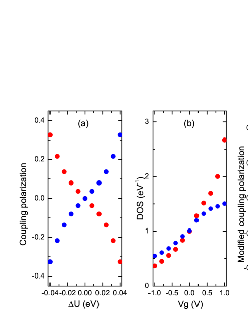
In figure 5(a), we plot the valley coupling polarization versus the gate voltage using the formula above. Similar to figure 2(b), we have . However, we also have a relation , i.e., are odd functions of which are different from our first principles results. In fact, from Eq. (12) one can easily get when . To understand this difference, we examine the contribution from DOS of the valence band which is not considered in KP model. Since the photoinduced current originates from the transition between different valence bands to the same conduction band we will neglect the influence of DOS of the conduction band. DOS near the top of valence band will be affected by the external electric field. Our ab initio results show that DOS of valence band are mainly contributed by Mo atoms of bilayer . From analytic calculation, we find that () is related mainly to DOS from lower (upper) layer of bilayer and () is related mainly to DOS from upper (lower) layer of bilayer . In figure 5(b), we plot the DOS of upper layer Mo atom (red dotted line) and lower layer Mo atom (blue dotted line) versus gate voltage obtained by ab initio method. From this figure, we see that the influence of external electric field on DOS of Mo atom of upper layer is different from that of lower layer. In another word, a better definition of valley coupling polarizations should include the effect of DOS as follows,
| (13) |
where and are DOS of lower and upper Mo atoms, respectively. In panel (c) of figure 5, we plot the modified coupling polarization as a function of using Eq. (13) with DOS taken from the panel (b) of figure 5. In order to compare with figure 3, we changed the abscissa of panel (c) from from -0.04 V to 0.04 V to from -1.0 V to 1.0 V according to our ab initio results. We see that the modified coupling polarization is no longer an odd function of the gate voltage, and the behaviors of for V are similar to the results in figure 3(b). In another word, by analyzing the polarization of coupling, one can get the information of the valley polarization. For the monolayer , one can directly using the KP model, but for the bilayer , one has to consider the influence of the DOS of the energy bands.
In summary, we have investigated the photoinduced current of layered as a function of external electric field. The results show that the valley polarization of photoinduced current of monolayer is independent of external electric field perpendicular to the surface of the layered which can be induced by the gate voltage, but the valley polarization of photoinduced current of bilayer is very sensitive to the external electric field that breaks the inversion symmetry. Moreover, the valley polarization can be tuned by changing the polarity of circular polarized light. The modulation of valley polarization of layered transistor by gate voltages and polarities of circular polarized light provide extra knot in future application of valleytronic devices.
This work was supported by National Natural Science Foundation of China (No.11374246, No.11574217, and No.11504240 ) and Shenzhen Natural Science Foundation (JCYJ20150324140036832).
References
- (1) Singh V et al 2011 Graphene based materials: Past, present and future Prog. Mater. Sci. 56 1178
- (2) Andrei E Y,Li G H and Du X 2012 Electronic properties of graphene: a perspective from scanning tunneling microscopy and magnetotransport Rep. Prog. Phys. 75 056501
- (3) Qiao Z and Ren Y F 2014 Recent progress on quantum anomalous Hall effect in graphene J. Shenzhen Univ. Sci. Eng. 31 551; Ren Y, Qiao Z and Niu Q 2015 Topological phases in two-dimensional materials: a brief review ariXiv:1509.09016v1
- (4) Bao Q L and Loh K P 2012 Graphene photonics, plasmonics, and broadband optoelectronic devices ACS Nano 6 3677
- (5) Novoselov K S et al 2005 Two-dimensional atomic crystals Proc. Natl. Acad. Sci. U.S.A. 102 10451
- (6) Lee C et al 2010 Frictional characteristics of atomically thin sheets science 328 76
- (7) Radisavljevic B, Radenovic A, Brivio J, Giacometti V and Kis A 2011 Single-layer MoS2 transistors Nat. Nanotechnol. 6 147
- (8) Korn T, Heydrich S, Hirmer M, Schmutzler J and Schuller C 2011 Low-temperature photocarrier dynamics in monolayer MoS2 Appl. Phys. Lett. 99 102109
- (9) Min H et al 2006 Intrinsic and Rashba spin-orbit interactions in graphene sheets Phys. Rev. B 74 165310
- (10) Yao Y G, Ye F, Qi X L, Zhang S C and Fang Z 2007 Spin-orbit gap of graphene: First-principles calculations Phys. Rev. B 75 041401
- (11) Zhu Z Y, Cheng Y C and Schwingenschlogl U 2011 Giant spin-orbit-induced spin splitting in two-dimensional transition-metal dichalcogenide semiconductors Phys. Rev. B 84 153402
- (12) Mak K F, Lee C, Hone J, Shan J and Heinz T F 2010 Atomically thin MoS2: A new direct-gap semiconductor Phys. Rev. Lett. 105 136805
- (13) Splendiani A et al 2010 Emerging photoluminescence in monolayer MoS2 Nano Lett. 10 1271
- (14) Rycerz A, Tworzydlo J and Beenakker C W J 2007 Valley filter and valley valve in graphene Nature Phys 3 172
- (15) Xiao D, Yao W and Niu Q 2007 Valley-contrasting physics in graphene: Magnetic moment and topological transport Phys. Rev. Lett. 99 236809
- (16) Zhang F, Jung J, Fiete G A, Niu Q and MacDonald A H 2011 Spontaneous quantum Hall states in chirally stacked few-layer graphene systems Phys. Rev. Lett. 106 156801
- (17) Xiao D, Liu G B, Feng W X, Xu X D and Yao W 2012 Coupled spin and valley physics in monolayers of MoS2 and other group-VI dichalcogenides Phys. Rev. Lett. 108 196802
- (18) Jones A M et al 2014 Spin-layer locking effects in optical orientation of exciton spin in bilayer WSe2 Nature Phys. 10 130
- (19) Yao W, Xiao D and Niu Q 2008 Valley-dependent optoelectronics from inversion symmetry breaking Phys. Rev. B 77 235406
- (20) Yuan H et al 2013 Zeeman-type spin splitting controlled by an electric field Nature Phys. 9 563
- (21) Zeng H L, Dai J F, Yao W, Xiao D and Cui X D 2012 Valley polarization in MoS2 monolayers by optical pumping Nat. Nanotech. 7 490
- (22) Wu S F et al 2013 Electrical tuning of valley magnetic moment through symmetry control in bilayer MoS2 Nature Phys. 9 149
- (23) Fontana M et al 2013 Electron-hole transport and photovoltaic effect in gated MoS2 Schottky junctions Sci. Rep. 3 1634
- (24) Lopez-Sanchez O, Lembke D, Kayci M, Radenovic A and Kis A 2013 Ultrasensitive photodetectors based on monolayer MoS2 Nat. Nanotech. 8 497
- (25) Sundaram R S et al 2013 Electroluminescence in Single Layer MoS2 Nano Lett. 13 1416
- (26) Yin Z Y et al 2012 Single-layer MoS2 phototransistors ACS Nano 6 74
- (27) Wu C C et al 2013 Elucidating the photoresponse of ultrathin MoS2 field-Effect transistors by scanning photocurrent microscopy J. Phys. Chem. Lett. 4 2508
- (28) Kadantsev E S and Hawrylak P 2012 Electronic structure of a single MoS2 monolayer Solid State Commun. 152 909
- (29) Liu Q H et al 2012 Tuning electronic structure of bilayer MoS2 by vertical electric field: A first-principles investigation J. Phys. Chem. C 116 21556
- (30) Lake R and Datta S 1992 nonequilibrium Greens-Function method applied to double-barrier resonant-tunneling diodes Phys. Rev. B 45 6670
- (31) Henrickson L E 2002 Nonequilibrium photocurrent modeling in resonant tunneling photodetectors J. Appl. Phys. 91 6273
- (32) Chen J Z, Hu Y B and Guo H 2012 First-principles analysis of photocurrent in graphene PN junctions Phys. Rev. B 85 155441
- (33) Kleinman L and Bylander D M 1982 efficacious form for model pseudopotentials Phys. Rev. Lett. 48 1425
- (34) Vignale G and Rasolt 1987 M Density-functional theory in strong magnetic-fields Phys. Rev. Lett. 59 2360
- (35) Taylor J, Guo H and Wang J 2001 Ab initio modeling of quantum transport properties of molecular electronic devices Phys. Rev. B 63 245407.
- (36) For details of the NanoDcal quantum tranpsort package,see http://www.nanoacademic.ca
- (37) Perdew J P and Wang Y 1992 Accurate and simple analytic representation of the electron-gas correlation-energy Phys. Rev. B 45 13244
- (38) Kubler J, Hock K H, Sticht J and Williams A R 1988 Density functional theory of non-collinear magnetism J. Phys. F 18 469
- (39) Kubler J, Hock K H, Sticht J and Williams A R 1988 Local spin-density functional theory of non-collinear magnetism J. Appl. Phys. 63 3482
- (40) Nordstrom L and Singh D J 1996 Noncollinear intra-atomic magnetism Phys. Rev. Lett. 76 4420
- (41) Zhang L et al 2014 Generation and transport of valley-polarized current in transition-metal dichalcogenides Phys. Rev. B 90 195428
- (42) Haug H and Jauho A P 1998 Quantum Kinetics in Transport and Optics of Semiconductors (Springer-Verlag,New York)
- (43) Gong Z R et al 2013 Magnetoelectric effects and valley-controlled spin quantum gates in transition metal dichalcogenide bilayers Nature Comm. 4 2053