Combined electrical transport and capacitance spectroscopy of a field effect transistor
Abstract
We have measured both the current-voltage (-) and capacitance-voltage (-) characteristics of a field effect transistor. From the measured capacitance we calculate the electron surface density and show that its gate voltage dependence follows the theoretical prediction resulting from the two-dimensional free electron model. This model allows us to fit the measured - characteristics over the entire range of . Combining this experimental result with the measured current-voltage characteristics, we determine the field effect mobility as a function of gate voltage. We show that for our device this improved combined approach yields significantly smaller values (more than a factor of 4) of the electron mobility than the conventional analysis of the current-voltage characteristics only.
After the rise of grapheneNovoselov et al. (2004, 2005a); Zhang et al. (2005), a wide range of two-dimensional (2D) materialsNovoselov et al. (2005b) shifted into focus of fundamental and applied researchFerrari et al. (2015). One particularly important class of 2D materials are transition metal dichalcogenides (TMDs)Wang et al. (2012). One important representative TMD is molybdenum disulfide, , whose indirect band gap changes to a direct one when its thickness is reduced to one single monolayer Mak et al. (2010); Splendiani et al. (2010). The resulting high optical activity and sizable bandgap of make this material ideally suited for optoelectronic applicationsLopez-Sanchez et al. (2013) and, thus the optical and electronic properties of and related materials have been investigated intensively in the last yearsSun, Martinez, and Wang (2016). In particular, field effect transistors (FETs) and logical circuit prototypes have been devised and realizedRadisavljevic et al. (2011); Radisavljevic, Whitwick, and Kis (2011); Fiori et al. (2014). In such devices, source and drain contacts are patterned onto the TMD film, and the charge carrier density is controlled by gate contacts. For FET devices, the transport mobility of the charge carriers in the conducting channel is of paramount importance. Here, different approaches exist to derive this key figure for FET devices. The most commonly applied method is to measure the source-drain current as a function of the gate voltage . Then, the field effect mobility is determined from a tangent to the linear region of the -dependence using the following formula known from FET theory:
| (1) |
Here, is the capacitance per unit area, the source-drain voltage, the slope of the linear region, the length and the width of the conducting channel. The intersection of the tangent with the abscissa represents the threshold voltage, . However, this simple FET formula (1) assumes that the mobility is independent of the gate voltage. Moreover, the underlying parallel-plate capacitor model used to quantify the capacitance Late et al. (2012); Radisavljevic et al. (2011) assumes perfectly conducting, infinitely large plates. These assumptions may represent an oversimplification for 2D semiconductors Fuhrer and Hone (2013); Radisavljevic and Kis (2013a). To quantify the capacitance more precisely, Radisavljevic and coworkers Radisavljevic and Kis (2013b) followed an indirect approach: the capacitance was determined from the carrier density obtained from Hall effect measurements and used in equation (1). This helps getting more reliable capacitance values than the ones from the parallel-plate capacitor formula, but the gate voltage dependence was not investigated.
In this Letter, we present an easy to implement approach to determine the carrier density and carrier mobility of a FET as a function of . For this purpose we combine standard with . The latter probes the carrier system at the chemical potential and allows us to directly derive the carrier density as a function of . All experimental data is found to be in excellent agreement with an analytical model based on a 2D electron system over the entire range of . Most strikingly we find that for our device the values of obtained solely from the overestimates those obtained taking into account the measure by more than a factor of .
The sample studied consists of -rotated, thick substrate of black lithium niobate (), on top of which a layer of has been deposited by chemical vapour deposition Nguyen et al. (2015); Preciado et al. (2015). We use such samples for investigations of the interaction of surface acoustic waves with , as described in ref. Preciado et al. (2015). The sample was characterized by mapping photoluminescence spectroscopy to confirm millimeter-scale growth of . FET devices were fabricated using an established processPreciado et al. (2015): the layer has been removed from the sample surface except of two stripes. This lithographically defined area includes the regions of highest emission intensity. On top of these stripes, two finger electrodes ( and ) with a distance of µ serve as source and drain contacts, contacting the two stripes along their entire width. The gate voltage was applied on the sample backside. A schematic of the sample is shown as inset in Fig. 1. All measurements have been performed under ambient conditions with the device mounted inside a sealed metal chip carrier to exclude any influences of external illumination.

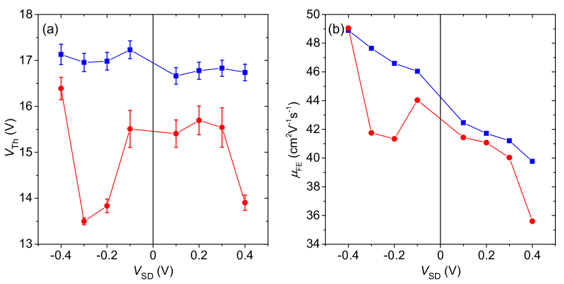
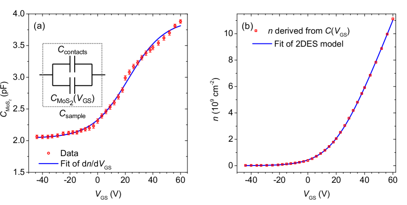
As a first estimate of , we measured the source-drain current at a fixed source-drain voltage as a function of , as depicted in Fig. 1. For each , a weak hysteresisLate et al. (2012) is resolved as the was scanned , which is less pronounced than that reported for a different sample in our previous workPreciado et al. (2015). The polarity of is chosen such that corresponds to negative charge on the layer. These characteristics directly confirm the accumulation of negative charge on the layer for . From this data, we extracted and using Eq. (1) and the simple parallel-plate capacitor model. The obtained values and are plotted as a function of as red symbols in Fig. 2 (a) and (b), respectively. Obviously, both the obtained values and their statistical errors exhibit significant scatter for the different values of . These shortcomings arise from the simple parallel-plate capacitor model and the fact that the -interval, in which the best fit of Eq. (1) is performed, is chosen by eye in the conducting region, so that all other data is neglected. We note, that this device shows similar characteristics as that reported in our previous workPreciado et al. (2015). In particular, lies in the same range. In order to improve our method, we directly quantify the capacitance between one contact and the back gate as a function of . is applied as a DC offset gate voltage to the capacitance bridge and modulated with a sine wave by the built-in oscillator. The measured capacitance was corrected for the capacitance of the wires connecting to the sample. In Fig. 3 (a), we plot the obtained capacitance of the sample (symbols) as a function of . For large negative , saturates at a constant value of . Under these conditions, the layer is completely depleted and the measured corresponds to that of the metal contacts , which is independent of . As increases, the surrounding 2D layer is populated with electrons and the capacitance increases as observed in the data. can be readily described as an equivalent circuit of connected in parallel with the -dependent capacitance of the TMD layer , shown as an inset of Fig. 3 (a). From we can directly calculate the electron surface density on the layer by a discrete integration. The symbols in Fig. 3 (b) are the result obtained from
with being the elementary charge.
The obtained values for faithfully reproduce a clear turn-on behavior and linear increase as expected for a FET.
We proceed by developing an analytical model of the -dependent electron density . The equilibrium electron density can be calculated by integrating the Fermi distribution function over the two-dimensional momenta ,
| (2) |
where is the spin and valley degeneracy for , , is the electron effective mass, the area of the monolayer, and the Planck constant; the energy is counted from the conduction band edge in MoS2. In the presence of a gate voltage the chemical potential in (2) should be modified as , where is the shift of in due to . We assume that is proportional to , i.e., and use the following function to fit our experimental data
| (3) |
with being a threshold voltage. The result of the best fit of this function to the derived from the measured capacitance is plotted as the solid line in Fig. 2(b) and shows that this analytical function perfectly follows the experimental data over the entire range of .
The values of the parameters and extracted from the fit are and . Since we get from the value of . Such a small value of suggests that the position of the electrochemical potential in the –metal contacts system is essentially determined by the contacts, where the density of states is substantially larger than in . Indeed, in equilibrium (without gate voltage) a small Schottky barrier, , is typically built up at the metal–TMD interface Yoon2011. Under these conditions, a certain amount of electrons flow into from the contacts, so that the density is inhomogeneous and larger in the near-contact areas than in the areas farther away. A positive increases the electron density in the top metal contact. The additional electrons accumulate at the bottom of the contact in a layer with a thickness corresponding to the Thomas-Fermi screening length, what leads to a small increase of the electrochemical potential in the –metal contacts system. Due to the high density of states in the metal, is much smaller than , which yields . Due to the growth of , more electrons flow into and larger areas of the 2D semiconductor become well-conducting. This basic physical picture qualitatively agrees with our results.
Comparing the equations (2) and (3), one can see that . Using extracted from and Yoon2011, one gets . In order to explain the deviation from the fit value, a more accurate model is necessary, which takes into account the concrete contact geometry and coordinate dependence.
An analytical expression for the capacitance can be directly obtained by taking the derivative of Eq.(3). We obtain
| (4) |
with being the maximum capacitance for .
The result of the best fit of Eq. (4) to the measured capacitance is shown as a solid line in Fig. 3 (a) which again faithfully reproduces the experimental data points.
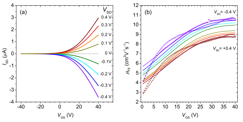
In the next step, we assume that is independent of . Thus, in the Drude model, can be fitted using Eq. (3). The results of such best fits for all measured are plotted as solid lines in Fig. 4 (a). Again, the fitted function faithfully reproduces the experimental data, underlining further the 2DES nature of the conducting channel. Furthermore, these obtained fit functions allow to determine and , using Eq. (1) with as the slope at large , with higher precision. The extracted values for and are plotted as blue symbols in Fig. 2 (a) and (b), respectively. Clearly, the scatter of the values derived from the fit results is dramatically reduced. We obtain , which is almost constant over the entire range of . In contrast, exhibits a clear trend to significantly decrease for increasing . The negative slope of the -dependence of the mobility has its reason in predominantly in hysteresis and drifts of the electrical characteristics. Both effects are commonly observed in such devicesLate et al. (2012); Illarionov et al. (2016).
Finally, we turn to carrier mobility and its dependence on the gate voltage, .
In the Drude model the conductivity is given by .
Thus, the mobility given by can be calculated only from measured data: can be derived from the characteristics [Figs. 1 and 4 (a)] and from the data [cf. Fig. 4 (b)].
We note that this analysis can be performed for our data only for . For negative both and vanish and any obtained value of exhibits a large error.
In Fig. 2 (b) we plot obtained directly from the measured (symbols) and the fitted (lines) characteristics for different values of for .
Remarkably, the absolute value of shown in Fig. 4 (b), which we obtained by including measured, realistic capacitance (and thereby ) data is significantly lower than that obtained from the basic parallel-plate capacitor model [cf. Fig. 2 (b)].
It ranges between and shows a pronounced increase with increasing (in addition to its global reduction as reduces [cf. Fig. 2 (b)]).
For , rapidly increases as the injected electrons screen scattering centers in the channel.
Such behavior is well established and has been observed for 2DES in established III-V semiconductor heterostructuresShayegan et al. (1988); Pfeiffer et al. (1989).
For this trend weakens and saturates.
This saturation behavior can be readily understood considering that as the chemical potential is fully shifted into the conduction band.
For large positive the chemical potential lies well above the random potential modulation induced by scattering centers.
Thus, any further increase of (i.e. ) does not lead to improved screening and, thus increased .
In summary, we demonstrated that combined electrical transport () and capacitance () spectroscopy allows to determine the field-effect mobility and threshold voltage of a TMD based FET with significantly higher precision than the commonly applied basic parallel-plate capacitor model.
We performed a three step analysis on model data of a - FET device starting with the basic parallel-plate capacitor model.
For our device the -dependent , and are in excellent agreement with an analytical model of an ideal 2DES over the entire range of .
This is in strong contrast to the basic parallel-plate capacitor model in which only data in a small, subjectively chosen interval of the -characteristics is considered.
The statistical errors of and can be significantly reduced by fitting and evaluating the -characteristics using our 2DES model as now the full data range is included.
Finally, by including the full -characteristics and the derived carrier density we are able to obtain the -dependent .
For our device we nicely observe a pronounced increase of at due to onset of efficient electrostatic screening.
Most strikingly, the absolute value of obtained this way is significantly lower than that obtained from the basic parallel-plate capacitor model.
Our full method is especially important for back-gated 2D material-based FETs.
For such devices, the distance between the 2D carrier system and the gate electrode is large compared to the lateral dimensions of typical flakes.
It enables (i) direct confirmation of 2DES-like character of the FET operation, and derive (ii) more accurate, realistic and (iii) -dependent values . Moreover, it does not require a magnetic field as the mobility determination via Hall effect, thus making it suitable for setups without magnets and for samples with low mobilities, for which the Hall angle is small.
This work was supported by the Deutsche Forschungsgemeinschaft (DFG) via the Emmy Noether Program (KR3790/2), by the Cluster of Excellence "Nanosystems Initiative Munich" (NIM), by the Bavaria-California Technology Center (BaCaTeC). L.B. thanks the National Science Foundation for support under NSF DMR 1609918 and C-SPIN, a STARnet center funded by MARCO and DARPA. E.P. and A.E.N. and G.S. gratefully acknowledge fellowship support through NSF DGE-1326120 and NSF DMR 1359136, respectively.
References
- Novoselov et al. (2004) K. S. Novoselov, A. K. Geim, S. V. Morozov, D. Jiang, Y. Zhang, S. V. Dubonos, I. V. Grigorieva, and A. A. Firsov, “Electric field effect in atomically thin carbon films,” Science 306, 666–669 (2004).
- Novoselov et al. (2005a) K. S. Novoselov, A. K. Geim, S. V. Morozov, D. Jiang, M. I. Katsnelson, I. V. Grigorieva, S. V. Dubonos, and A. A. Firsov, “Two-dimensional gas of massless Dirac fermions in graphene,” Nature 438, 197–200 (2005a).
- Zhang et al. (2005) Y. Zhang, Y.-W. Tan, H. L. Stormer, and P. Kim, “Experimental observation of the quantum Hall effect and Berry’s phase in graphene,” Nature 438, 201–204 (2005).
- Novoselov et al. (2005b) K. S. Novoselov, D. Jiang, F. Schedin, T. J. Booth, V. V. Khotkevich, S. V. Morozov, and A. K. Geim, “Two-dimensional atomic crystals,” Proceedings of the National Academy of Sciences of the United States of America 102, 10451–10453 (2005b).
- Ferrari et al. (2015) A. C. Ferrari, F. Bonaccorso, V. Fal’ko, K. S. Novoselov, S. Roche, P. Boggild, S. Borini, F. H. L. Koppens, V. Palermo, N. Pugno, J. A. Garrido, R. Sordan, A. Bianco, L. Ballerini, M. Prato, E. Lidorikis, J. Kivioja, C. Marinelli, T. Ryhanen, A. Morpurgo, J. N. Coleman, V. Nicolosi, L. Colombo, A. Fert, M. Garcia-Hernandez, A. Bachtold, G. F. Schneider, F. Guinea, C. Dekker, M. Barbone, Z. Sun, C. Galiotis, A. N. Grigorenko, G. Konstantatos, A. Kis, M. Katsnelson, L. Vandersypen, A. Loiseau, V. Morandi, D. Neumaier, E. Treossi, V. Pellegrini, M. Polini, A. Tredicucci, G. M. Williams, B. Hee Hong, J.-H. Ahn, J. Min Kim, H. Zirath, B. J. van Wees, H. van der Zant, L. Occhipinti, A. Di Matteo, I. A. Kinloch, T. Seyller, E. Quesnel, X. Feng, K. Teo, N. Rupesinghe, P. Hakonen, S. R. T. Neil, Q. Tannock, T. Lofwander, and J. Kinaret, “Science and technology roadmap for graphene, related two-dimensional crystals, and hybrid systems,” Nanoscale 7, 4598–4810 (2015).
- Wang et al. (2012) Q. H. Wang, K. Kalantar-Zadeh, A. Kis, J. N. Coleman, and M. S. Strano, “Electronics and optoelectronics of two-dimensional transition metal dichalcogenides,” Nature Nanotechnology 7, 699–712 (2012).
- Mak et al. (2010) K. F. Mak, C. Lee, J. Hone, J. Shan, and T. F. Heinz, “Atomically thin : A new direct-gap semiconductor,” Physical Review Letters 105, 136805 (2010).
- Splendiani et al. (2010) A. Splendiani, L. Sun, Y. Zhang, T. Li, J. Kim, C.-Y. Chim, G. Galli, and F. Wang, “Emerging photoluminescence in monolayer MoS2.” Nano Letters 10, 1271–5 (2010).
- Lopez-Sanchez et al. (2013) O. Lopez-Sanchez, D. Lembke, M. Kayci, A. Radenovic, and A. Kis, “Ultrasensitive photodetectors based on monolayer MoS2,” Nature Nanotechnology 8, 497–501 (2013).
- Sun, Martinez, and Wang (2016) Z. Sun, A. Martinez, and F. Wang, “Optical modulators with 2D layered materials,” Nature Photonics 10, 227–238 (2016).
- Radisavljevic et al. (2011) B. Radisavljevic, A. Radenovic, J. Brivio, V. Giacometti, and A. Kis, “Single-layer transistors,” Nature Nanotechnology 6, 147–150 (2011).
- Radisavljevic, Whitwick, and Kis (2011) B. Radisavljevic, M. B. Whitwick, and A. Kis, “Integrated circuits and logic operations based on single-layer ,” ACS nano 5, 9934–9938 (2011).
- Fiori et al. (2014) G. Fiori, F. Bonaccorso, G. Iannaccone, T. Palacios, D. Neumaier, A. Seabaugh, S. K. Banerjee, and L. Colombo, “Electronics based on two-dimensional materials,” Nature Nanotechnology 9, 768–779 (2014).
- Late et al. (2012) D. J. Late, B. Liu, H. S. S. R. Matte, V. P. Dravid, and C. N. R. Rao, “Hysteresis in single-layer field effect transistors,” ACS Nano 6, 5635–5641 (2012).
- Fuhrer and Hone (2013) M. S. Fuhrer and J. Hone, “Measurement of mobility in dual-gated transistors,” Nature Nanotechnology 8, 146–147 (2013).
- Radisavljevic and Kis (2013a) B. Radisavljevic and A. Kis, “Reply to "measurement of mobility in dual-gated transistors",” Nature Nanotechnology 8, 147–148 (2013a).
- Radisavljevic and Kis (2013b) B. Radisavljevic and A. Kis, “Mobility engineering and a metal–insulator transition in monolayer ,” Nature Materials 12, 815–820 (2013b).
- Nguyen et al. (2015) A. Nguyen, P. Sharma, T. Scott, E. Preciado, V. Klee, D. Sun, I.-H. D. Lu, D. Barroso, S. Kim, V. Y. Shur, A. R. Akhmatkhanov, A. Gruverman, L. Bartels, and P. A. Dowben, “Toward ferroelectric control of monolayer ,” Nano Letters 15, 3364–3369 (2015).
- Preciado et al. (2015) E. Preciado, F. J. Schülein, A. E. Nguyen, D. Barroso, M. Isarraraz, G. von Son, I.-H. Lu, W. Michailow, B. Möller, V. Klee, J. Mann, A. Wixforth, L. Bartels, and H. J. Krenner, “Scalable fabrication of a hybrid field-effect and acousto-electric device by direct growth of monolayer ,” Nature Communications 6, 8593 (2015).
- Illarionov et al. (2016) Y. Y. Illarionov, G. Rzepa, M. Waltl, T. Knobloch, A. Grill, M. M. Furchi, T. Mueller, and T. Grasser, “The role of charge trapping in MoS 2 /SiO 2 and MoS 2 /hBN field-effect transistors,” 2D Materials 3, 035004 (2016).
- Shayegan et al. (1988) M. Shayegan, V. J. Goldman, C. Jiang, T. Sajoto, and M. Santos, “Growth of low-density two-dimensional electron system with very high mobility by molecular beam epitaxy,” Applied Physics Letters 52, 1086 (1988).
- Pfeiffer et al. (1989) L. Pfeiffer, K. W. West, H. L. Stormer, and K. W. Baldwin, “Electron mobilities exceeding in modulation-doped GaAs,” Applied Physics Letters 55, 1888 (1989).