Thermal relaxation in titanium nanowires: signatures of inelastic electron-boundary scattering in heat transfer
Abstract
We have employed noise thermometry for investigations of thermal relaxation between the electrons and the substrate in nanowires patterned from 40-nm-thick titanium film on top of silicon wafers covered by a native oxide. By controlling the electronic temperature by Joule heating at the base temperature of a dilution refrigerator, we probe the electron-phonon coupling and the thermal boundary resistance at temperatures Kelvin. Using a regular -dependent electron-phonon coupling of clean metals and a -dependent interfacial heat flow, we deduce a small contribution for the direct energy transfer from the titanium electrons to the substrate phonons due to inelastic electron-boundary scattering.
I Introduction
Thermal properties of nanoscale structures and their particular energy relaxation processes form a key issue for various practical applications ranging from quantum computing to ultra sensitive radiation detectors and quantum-limited calorimeters. By providing the major mechanism for heat transfer between electrons and phonons at typical cryogenic temperatures Lounasmaa (1974), the inelastic electron-phonon scattering determines the effective temperature of the electron sub-system, and it plays an essential role in the operation of different low-temperature micro and nano devices. Optimization, or preferably tuning, of this parameter in a wide range sets the basis for successful development and improvement of sensitivity of a vast class of devices.
Thermal relaxation of electrons in metallic cryogenic nanodevices takes place typically either by electronic diffusion or by electron – phonon coupling (e-ph). The e-ph relaxation processes lead to a temperature-dependent thermal conductance which varies with the temperature in a power law fashion where Giazotto et al. (2006) and denotes the temperature difference between the electrons and phonons. The heat flow due to the e-ph coupling may lead to an overheated state of the phonons in the metallic conductor owing to the Kapitza resistance between the phonon systems of the dielectric substrate and the metal. In addition to the regular Kapitza resistance , there may also be a direct electronic heat transfer channel from the electrons to the substrate phonons Huberman and Overhauser (1994); Sergeev (1998); Mahan (2009); Low et al. (2012). In clean systems, this direct coupling facilitated by the inelastic electron-boundary scattering has the same form as the Kapitza-resistance-limited heat conductance, in which the phonon temperature of the hot side is replaced by the electron temperature. The relative strength of these two parallel heat transfer channels across the film-dielectric interface is an open question, and this issue forms the main objective of the present study.
We have chosen thin, narrow titanium wires for our studies. Titanium metal has been successfully employed in various ultrasensitive hot-electron bolometers both in the superconducting and normal states Wei et al. (2008); Karasik et al. (2011). In spite of the quite intensive experimental studies of thermal relaxation in titanium micro and nanostructures Wu et al. (1998); Hsu et al. (1999); Manninen et al. (1999); Gershenson et al. (2001); Horn and Harrison (2003); Fukuda et al. (2007); Karasik et al. (2007); Wei et al. (2008); Day et al. (2008); Karasik et al. (2009), the reported results for titanium and its alloys distinctly vary both in their absolute magnitude as well as in their functional form Karvonen et al. (2005); Karasik et al. (2011).
We study titanium nanowires having cross sections, thickness width , of about nm2, and find the best-fit exponent in the electron – subsrate phonon heat conductance law to be close to . Such an observation is consistent with the predictions for the electron – phonon coupling in disordered metallic films as well as with the behavior governed by Kapitza resistance. Our analysis of the electron relaxation and thermal balance in Ti wires is based on a model that includes the overheated state of the phonons with an intermediate temperature in the film as well as the direct energy transfer from the electrons to the substrate phonons via inelastic electron scattering at the film-substrate boundary. Our model allows for investigations of the cross-over behavior between the distinct power law regimes which are dominated by different relaxation processes. Using such a model with realistic materials parameters, we obtain evidence for a weak contribution of the inelastic electron-boundary scattering. Our result is obtained at temperatures between K and K in a regime where the Kapitza resistance between the film and the substrate phonons reduces the major heat flow mediated by the regular electron-phonon coupling. However, as this Kapitza resistance is poorly known, we also discuss other possible interpretations of our data, such as a modification of the electron-phonon coupling due to disorder, yielding a different value for the exponent .
II Thermometry and heat transfer
Our experiment relies on the sensitivity of noise thermometry of electrons in nanoscale samples Wu et al. (2010); Chaste et al. (2010); Santavicca et al. (2010). Noise thermometry in quasi-equilibrium is possible when the electron-electron scattering is strong and a local, spatially varying temperature profile can be defined Blanter and Büttiker (2000). The average effective temperature is related to the bias voltage via where the Fano factor is given by the current noise power spectrum and the current through the sample is . Using the diffusion constant m2/s obtained from the electron mean free path of 2.5 nm and the Fermi velocity of 300 km/s Sanborn et al. (1989), we obtain for the electron-electron (e-e) interaction length m at K (the worst case estimate corresponding to the maximum length). As , we are in the strong electron-electron interaction regime (the hot electron regime), and the Fano factor becomes . The value of remains constant till the inelastic processes start to remove energy from the electronic system. The proportionality given by the Fano factor between the effective temperature and the bias is also valid in the high-bias regime where the electron-phonon scattering dominates the heat transfer Wu et al. (2010). This is because the noise power and the related are connected by an effective Johnson noise relation. Recently, noise thermometry has been utilized in the studies of novel nanoscale systems when the implementation of regular thermometry is problematic Tarkiainen et al. (2003); Wu et al. (2010); Chaste et al. (2010); Santavicca et al. (2010); Fong and Schwab (2012); Laitinen et al. (2014); McKitterick et al. (2014).
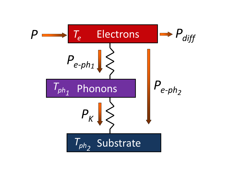
The Joule heating power, in a wire with resistance , can be dissipated into phonons via the electron–phonon (e-ph) interaction. The poor coupling of the film phonons with the substrate phonons will affect the e-ph scattering rates and, consequently, influence the electron temperature once the e-ph scattering becomes stronger than the e-e scattering. Here, we employ the energy balance model for the sample electron – sample phonon – substrate phonon coupling Bron and Grill (1977); Roukes et al. (1985); Wellstood et al. (1994); Bergmann et al. (1990) schematically presented in Fig. 1, including also the inelastic electron-boundary scattering that couples electrons directly to the substrate phonons Huberman and Overhauser (1994); Sergeev (1998). In this model, the ratio of to determines the crossover from the nearly parabolic temperature profile in the hot electron regime to a more constant profile in the case of strong electron-phonon scattering. In our analysis of the significant part of the wire (see Sect IIIB), we assume , which is valid only in the strong bias regime. The temperature dependence can be obtained from the Wiedemann-Franz law utilizing the measured resistance of the wire.
Apart form the electronic heat diffusion, is determined by the three thermal resistances responsible for (a) the heat exchange between the electrons and phonons in the conductor ( in Fig. 1), (b) the acoustic coupling between the phonons in the metallic conductor and the phonons in the insulating substrate (), and (c) the coupling between the electrons in the metallic conductor and the phonons in the insulating substrate (). When , the power-law exponent (see below) is determined by the dominating thermal resistance along the main heat flow path.
In regular metals, the power flow between the electron and phonon systems, corresponding to in Fig. 1 can be expressed as follows Kaganov et al. (1957); Allen (1987); Giazotto et al. (2006):
| (1) |
where denotes the phonon temperature, is a material-dependent coupling coefficient, is the volume of the sample, and is the exponent specified by the electron-phonon scattering rate . Nowadays, it is commonly accepted that, in clean metals, the electron-phonon scattering rate is proportional to Tp with Roukes et al. (1985); Wellstood et al. (1994); Sergeev and Mitin (2000). Similar behavior is also observed in thin metallic films Giazotto et al. (2006), including titanium. In our analysis, we take Wm-3K-5 from Ref. Manninen et al., 1999.
The physics of the e-ph coupling becomes more complicated in dirty metals Sergeev and Mitin (2000) or in systems with a restricted geometry where the electron-phonon scattering or/and the phonon spectrum Karvonen and Maasilta (2007) can significantly be modified compared to the bulk materials in the clean limit. In disordered systems, the electron-phonon scattering rate follows T2 or the T4 ( or 4) law depending on the scattering mechanisms Sergeev and Mitin (2000). Evidence of in disordered films has been obtained, for example, in Nb and Ti Gershenzon et al. (1990); Wei et al. (2008).
In clean metals, the dimensionality of the sample may lead to a modification of the electron-phonon relaxation time due to a reduction in the available phonon modes. According to the Debye model Kittel (2005), the change of the acoustic phonon spectrum from 3D to 2D leads to a weaker temperature dependence of the electron-phonon power flow, namely to a law where is the phonon dimensionality DiTusa et al. (1992). Evidence of this behavior has been obtained in Ref. Karvonen and Maasilta, 2007.
The Kapitza thermal boundary resistance originates from the mismatch of acoustic properties across an interfacial boundary, leading to a phonon temperature difference between the two materials . The corresponding power flow through the interface can be expressed as Pollack (1969); Lounasmaa (1974):
| (2) |
where the coupling coefficient has been expressed in terms of the linearized Kapitza conductance of the interface between the two materials and the area of the interface . Typically, the coefficient varies between and Wm-2K-4 for the common metal-to-dielectric interfaces used in microfabricated systems Swartz and Pohl (1989). The standard value for the Kapitza conductance between a metallic film and the common dielectrics amounts to Wm-2K-4 Roukes et al. (1985); Taskinen (2006). In our wire geometry with a nearly square-shaped cross section, we have adopted the Kapitza conductance , where the factor of two approximates the reduction of the effective phonon modes in the wire geometry. The reduction value reflects ray-tracing of phonons, where the propagation angles exceeding cannot fully escape the wire without collisions with the edges. Even a larger loss of coupling would be obtained if van Hove singularities in the phonon density of states are taken in to account, in a similar fashion as is predicted for the electron-phonon coupling in reduced dimensions Bilotsky and Tomchuk (2008).
The inelastic electron scattering at the interface between a metallic film and an insulating substrate may provide an additional channel for the energy transfer from electrons to the phonons of the substrate Huberman and Overhauser (1994); Sergeev (1998), proportional to . At low temperatures near equilibrium, the contribution to the interfacial "electronic Kapitza" thermal conductance is given by Sergeev (1998)
| (3) |
where and are the longitudinal and transverse sound velocities, respectively, and is the Sommerfeld constant. If in a metal , then this inelastic electron-boundary scattering contribution to the interfacial thermal conductance has the same temperature dependence as the regular acoustic phonon-phonon Kapitza term. The mechanism can be significant in those metallic films which have a strong electron-phonon coupling. The estimations for our samples based on Eq. 3 using from Ref. Manninen et al., 1999 yield to Wm-2K-4. However, since Eq. 3 has been derived ignoring the reduction of the electron-phonon coupling near the interface, we regard as a poorly known parameter and expect its actual magnitude to be smaller, possibly a few times smaller, than evaluated from the above equation.
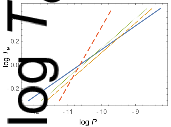
The different heat flow terms for a Ti wire with a cross section of nm2 and having a length of m are illustrated in Fig. 2. In addition to the contributions , , and , we depict also the outdiffusion of heat ; the large ratio of excludes any substantial phonon conductance along the wire. According to the comparison, we expect initially a regime governed by the electronic heat diffusion, which crosses over to the Kapitza resistance limited regime above K. The direct coupling of electrons to the substrate phonons given by the theoretical formula in Eq. 3 is indicated by the dashed-dotted line. In our analysis, we use literature values for the term Manninen et al. (1999) while for we employ a semiempirical value based on Refs. Roukes et al., 1985 and Bilotsky and Tomchuk, 2008, which leaves only the magnitude of as a parameter to fit to the data.
III Thermal modeling
III.1 Two temperature model: Hot phonons in the wire
To clarify our thermal model based on Fig. 1, we consider a long, voltage-biased normal wire coupled to the films of the same thickness on both sides. We assume that the electronic thermal diffusion of heat can be neglected at high bias, i.e., the electronic temperature inside the wire, , is constant as dominates the heat conduction. The Joule heat generated in the wire per unit volume, , is first transferred to the phonon heat bath inside the wire, which is characterized by the temperature ,
| (4) |
where is the conductivity. At the second stage, the phonons are cooled via the Kapitza conductance mechanism
| (5) |
Here is the base temperature. Using Eqs. 4 and 5, we can solve for the electronic temperature
| (6) |
This formula is fitted to our data in Fig. 5. The role of the direct electron-phonon contribution is to lower the heat flow in Eq. 6. For simplicity, we employ the ratio for the reduction factor which is valid in the high-temperature limit.
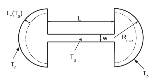
III.2 Analysis of thermal gradients
Besides the assumption in the narrow wire part, our analysis assumes that the scale of the relaxation of in the overheated wide sections of the leads is so short that the effective thermal noise of the leads can be neglected. To justify this assumption, we derive a characteristic length scale for the temperature drop at the ends of the wire. We consider a normal wire coupled to the two wide normal leads on both sides as depicted in Fig. 3. The wire and the leads are made of the same film thickness . We assume that at some large distance, , from the wire ends the temperature of the leads becomes equal to the temperature of the substrate mK.
The temperature both in the wire and in the leads can be found from the equation
| (7) |
where we have approximated the experimentally determined heat flow by the formula per unit volume (see Sect. V), and is the current density. Inside the wire while in the lead at a distance from the end of the wire. At a sufficiently high bias, the temperature in the leads in the vicinity of the wire ends equals to
| (8) |
At some distance the temperature drops to the equilibrium value . The characteristic length scale at which this happens is , where
| (9) |
is the temperature relaxation length. Since the resistance of the wire, , is much higher than the resistance of the leads, , the noise in this regime may be approximated as , i.e. the noise from the end sections can be neglected. This analysis is consistent if , which is satisfied at a sufficiently large Joule heating. The values of the relaxation length at K, which is a typical value of the temperature in the experiment, are listed in Table 1.
IV Experimental procedures
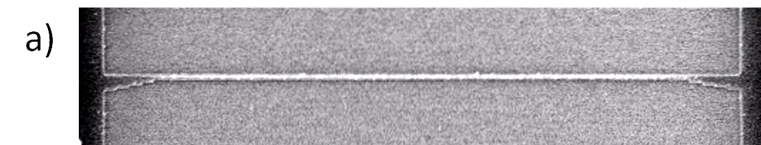
Our Ti wires were evaporated from a 99.999% titanium source in a high-quality e-gun evaporator at pressures below mBar. High-resistivity silicon wafers ( kcm) with a natural oxide layer were used as the insulating substrate. The samples were fabricated using a lift-off process based on e-beam lithography and a PMMA resist mask. Fig. 4a displays an SEM image of a typical structure. Sample B (see Table I) was measured without any additional processing steps. Samples A and C were cleaned using ion milling to reduce the cross section of the nanowire Zgirski et al. (2008). As a byproduct of the ion milling process, the sample surfaces became efficiently polished down to 1 nm scales. The basic parameters of the measured samples are specified in Table I. The bonding pads on the sample chip were m2.
| Dimensions nm3 | Rn | Ic | treatment | |||
| A | 50 40 10,000 | 4 k | 10 nA | 2.7 m | 0.25 K | sputtered |
| B | 43 40 10,000 | 7 k | 7 nA | 2.7 m | 0.10 K | not etched |
| C | 38 40 10,000 | 5 k | 9 nA | 3.7 m | 0.16 K | sputtered |
The length of our wires was chosen to be quite long (10 m) in order to alleviate the influence of the temperature gradients at the ends of the wires on the analysis and to reduce the influence of the longitudinal electronic heat diffusion along the wire. The samples were mounted on a copper sample holder in a Bluefors LD250 3He/4He dilution refrigerator with a base temperature of 10 mK. The heating power applied to the electron system of the nanowire was calculated from the applied electrical current and the wire resistance. The effective noise temperature scale was calibrated against the shot noise of an aluminum oxide tunnel junction; the scale was verified against the effective thermal noise in the hot electron regime.
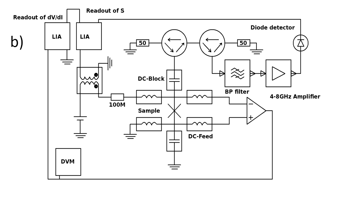
The electric measurement setup is schematically presented in Fig. 4b. By employing both low and high frequency coupling components, the setup facilitates audio-frequency conductance measurements and, simultaneously, a recording of current fluctuations at GHz-frequency. Two bias-Ts and two inductors are connected to the sample in order to measure the low-frequency AC conductance with a lock-in amplifier (LIA) in a four probe configuration. Two coupling capacitors are connected to the ends of the sample in order to couple the high-frequency current fluctuations to the 50 Ohm measurement cables. Good coupling of the sample noise to the 50 system was ensured by using short bond wires and by avoiding capacitive shunting in the pad and lead structures on the chip. Two 4-8 GHz circulators in series and a corresponding band pass filter (with a 0.5-dB pass band loss) are employed to block the backaction noise of the cryogenic HEMT amplifier (Low Noise Factory, LNF-LNC4_8A) from reaching the sample, which is of particular importance when checking for superconducting properties of nanoscale systems. The detection of noise over the spectrometer bandwidth of GHz 111Due to the bandpass filter in the output line and the frequency dependence of attenuation, the effective band width as referred to the maximum gain is reduced by a factor of two. is performed using a square-law diode detector (Krytar 203BK Schottky diode). A second lock-in amplifier is recording differential current-induced noise which can be integrated to yield the excess current noise at current . The operation with AC-current modulation reduces possible drift in the gain of the HEMT amplifier which easily hampers the performance of a noise spectrometer Nieminen et al. (2016).
V Results
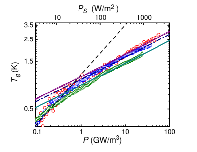
Fig. 5a displays the dependence of the effective electron temperature in the titanium nanowire as function of the applied power density in W/m3, and also as a function of the power per contact area W/m2 (top axis). We display our data at K only, since the behaviour of below K was dominated by the electronic heat diffusion and it was influenced by the superconducting transition, the critical temperature of which slightly varied between the Ti samples (see Table I). At K, the temperature dependence in each sample demonstrates a nearly linear behaviour on the log-log scale. The dashed line in Fig. 5 with indicates the behavior of the hot electron regime with with . The data agree quite well with the hot electron behavior of at bias voltages mV, which also lends support to the correctness of the employed effective noise temperature scale.
Three curves based on Eq. 6 are displayed in Fig. 5a, two with and one without the heat flow contribution due to . A better agreement is obtained with the term included. The obtained values for the conductance due to the inelastic electron-boundary scattering Huberman and Overhauser (1994); Sergeev (1998) are given in Table II. On the average, the obtained value Wm-2K-4 is nearly by an order of magnitude smaller than that evaluated from Eq. 3.
| Width (nm) | (Wm-2K-4) | (Wm-2K-4) | (Wm-3K-4) | |
|---|---|---|---|---|
| A | 50 | 340 | 200 | |
| B | 43 | 220 | 55 | |
| C | 38 | 180 | 0 |
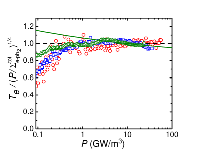
Fig. 5b analyzes small deviations from the dependence. In Fig. 5b we scale the measured electronic temperature by the heat power dependent product . The obtained ratio remains almost constant within two orders of magnitude of the applied power. The decrease in the data below 1 at small power GW/m3 is due to the crossover to the hot electron regime. A gradual small decrease is found at large Joule heating, which agrees with the theoretical curve derived from the two-temperatures-in-series model. The fitted curve, calculated using Eq. 6, displays a decrease that agrees well with the data. This agreement indicates to us that the standard channel via overheated film phonons and Kapitza resistance plays a role in the heat transport to substrate phonons 222The possible power flow limitation by or at the lowest temperatures is not accessible in our experiment due to the large diffusive term .
We note that our results can be lumped to a single electron-phonon coupling term of the form per unit volume; the values for the effective coupling constant are given in Table II. The variation of this parameter could be assigned to the different levels of disorder in each particular sample: e.g. the surface roughness and/or quality of the nanostructure-substrate interface. Neglecting the Kapitza resistance, i.e. setting , this kind of a description would agree with the earlier electron-phonon coupling work on Ti films where the observed behavior was assigned to the disorder in the films Wei et al. (2008); Karasik et al. (2011).
VI Discussion
From the comparison of the theoretical formulas and the measured data, it is evident that an unambiguous identification of the heat flow contributions in our Ti wire relaxation is not possible. We can only provide a consistent picture based on the previous experimental works as discussed in the description of the analysis of our results. Additional work would be needed to reach more definite conclusions concerning the relevant terms and their relative magnitudes. In general, the thermal resistance between the phonons in metallic films and the substrate at low temperatures is significantly smaller than the electron-phonon thermal resistance Roukes et al. (1985); Wellstood et al. (1989); Echternach et al. (1992). However, this condition is violated already in 100-nm copper films at electronic temperatures above mK Roukes et al. (1985); Taskinen (2006). Hence, it is quite ordinary that, in a sample like ours, the Kapitza resistance becomes relevant in the experiments performed at K.
As already noted, we could optionally assign all our observations to heat relaxation by the electron-phonon scattering in the bulk. In this view, the electron-phonon term would be dominated by static impurities Sergeev and Mitin (2000) leading to a similar dependence as there exists for the Kapitza-limited heat flow with per unit area. The effective coupling constant would then become equal to and there would be no way to separate between these two contributions from each other. Neglecting the Kapitza resistance and the term , we find Wm-3K-4, the magnitude of which is close to the values reported in Ref. Wei et al., 2008.
Our heat relaxation results are relevant also to quasi-one-dimensional superconductors Arutyunov et al. (2008). The issue of energy dissipation in the resistive state of a superconductor is intimately linked with the relaxation of the Joule heating of the same system in the normal state. Rapid heat relaxation in narrow titanium nanowires in the normal state is essential for obtaining single-quantum phase slip events in the superconducting state Lehtinen et al. (2012a, b). According to our results, a reduction of the Kapitza resistance between the film and the substrate could enhance the relaxation speed of the film and thereby help in the nucleation of fully uncorrelated quantum phase slips.
In conclusion, our experimental analysis indicates that distinguishing the different heat flow contributions in narrow Ti wires is an intriguing issue and several assumptions have to be made in order to extract values for the separate contributions. Extensive additional experiments are needed in order to elaborate these issues further.
Acknowledgements
This work was supported by the Academy of Finland (grant no. 284594, LTQ CoE), and by the European Research Council (grant no. 670743). This research made use of the OtaNano Low Temperature Laboratory infrastructure of Aalto University, that is part of the European Microkelvin Platform. Konstantin Arutyunov acknowledges the support of the Russian Science Foundation grant No. 16-12-10521.
References
- Lounasmaa (1974) O. V. Lounasmaa, Experimental Principles and Methods Below 1 K (Academic Press, New York, 1974).
- Giazotto et al. (2006) F. Giazotto, T. T. Heikkilä, A. Luukanen, A. M. Savin, and J. P. Pekola, Rev. Mod. Phys. 78, 217 (2006).
- Huberman and Overhauser (1994) M. L. Huberman and A. W. Overhauser, Phys. Rev. B 50, 2865 (1994).
- Sergeev (1998) A. V. Sergeev, Phys. Rev. B 58, R10199 (1998).
- Mahan (2009) G. D. Mahan, Phys. Rev. B 79, 075408 (2009).
- Low et al. (2012) T. Low, V. Perebeinos, R. Kim, M. Freitag, and P. Avouris, Phys. Rev. B 86, 045413 (2012).
- Wei et al. (2008) J. Wei, D. Olaya, B. S. Karasik, S. V. Pereverzev, A. V. Sergeev, and M. E. Gershenson, Nat. Nanotechnol. 3, 496 (2008).
- Karasik et al. (2011) B. S. Karasik, A. V. Sergeev, and D. E. Prober, IEEE Trans. Terahertz Sci. Technol. 1, 97 (2011).
- Wu et al. (1998) C. Y. Wu, W. B. Jian, and J. J. Lin, Phys. Rev. B 57, 11232 (1998).
- Hsu et al. (1999) S. Y. Hsu, P. J. Sheng, and J. J. Lin, Phys. Rev. B 60, 3940 (1999).
- Manninen et al. (1999) A. J. Manninen, J. K. Suoknuuti, M. M. Leivo, and J. P. Pekola, Appl. Phys. Lett. 74, 3020 (1999).
- Gershenson et al. (2001) M. E. Gershenson, D. Gong, T. Sato, B. S. Karasik, and A. V. Sergeev, Appl. Phys. Lett. 79, 2049 (2001).
- Horn and Harrison (2003) R. Horn and J. P. Harrison, J. Low Temp. Phys. 133, 291 (2003).
- Fukuda et al. (2007) D. Fukuda, R. M. T. Damayanthi, A. Yoshizawa, N. Zen, H. Takahashi, K. Amemiya, and M. Ohkubo, IEEE Trans. Appl. Supercond. 17, 259 (2007).
- Karasik et al. (2007) B. S. Karasik, D. Olaya, J. Wei, S. Pereverzev, M. E. Gershenson, J. H. Kawamura, W. R. McGrath, and A. V. Sergeev, IEEE Trans. Appl. Supercond. 17, 293 (2007).
- Day et al. (2008) P. Day, H. G. Leduc, C. D. Dowell, R. A. Lee, A. Turner, and J. Zmuidzinas, J. Low Temp. Phys. 151, 477 (2008).
- Karasik et al. (2009) B. S. Karasik, S. V. Pereverzev, D. Olaya, J. Wei, M. E. Gershenson, and A. V. Sergeev, IEEE Trans. Appl. Supercond. 19, 532 (2009).
- Karvonen et al. (2005) J. T. Karvonen, L. J. Taskinen, and I. J. Maasilta, Phys. Rev. B 72, 012302 (2005).
- Wu et al. (2010) F. Wu, P. Virtanen, S. Andresen, B. Plaçais, and P. J. Hakonen, Appl. Phys. Lett. 97, 262115 (2010).
- Chaste et al. (2010) J. Chaste, E. Pallecchi, P. Morfin, G. Feve, T. Kontos, J. M. Berroir, P. Hakonen, and B. Plaçais, Appl. Phys. Lett. 96, 192103 (2010).
- Santavicca et al. (2010) D. F. Santavicca, J. D. Chudow, D. E. Prober, M. S. Purewal, and P. Kim, Nano Lett. 10, 4538 (2010).
- Blanter and Büttiker (2000) Y. M. Blanter and M. Büttiker, Prog. Reports Phys. 336, 1 (2000).
- Sanborn et al. (1989) B. A. Sanborn, P. B. Allen, and D. A. Papaconstantopoulos, Phys. Rev. B 40, 6037 (1989).
- Tarkiainen et al. (2003) R. Tarkiainen, M. Ahlskog, P. Hakonen, and M. Paalanen, J. Phys. Soc. Japan 72, 100 (2003).
- Fong and Schwab (2012) K. C. Fong and K. C. Schwab, Phys. Rev. X 2, 31006 (2012).
- Laitinen et al. (2014) A. Laitinen, M. Oksanen, A. Fay, D. Cox, M. Tomi, P. Virtanen, and P. J. Hakonen, Nano Lett. 14, 3009 (2014).
- McKitterick et al. (2014) C. B. McKitterick, H. Vora, X. Du, B. S. Karasik, and D. E. Prober, J. Low Temp. Phys. 176, 291 (2014).
- Bron and Grill (1977) W. E. Bron and W. Grill, Phys. Rev. B 16, 5303 (1977).
- Roukes et al. (1985) M. L. Roukes, M. R. Freeman, R. S. Germain, R. C. Richardson, and M. B. Ketchen, Phys. Rev. Lett. 55, 422 (1985).
- Wellstood et al. (1994) F. C. Wellstood, C. Urbina, and J. Clarke, Phys. Rev. B 49, 5942 (1994).
- Bergmann et al. (1990) G. Bergmann, W. Wei, Y. Zou, and R. M. Mueller, Phys. Rev. B 41, 7386 (1990).
- Kaganov et al. (1957) M. I. Kaganov, I. M. Lifshitz, and I. V. Tanatarov, Sov. Phys. JETP 4, 173 (1957).
- Allen (1987) P. B. Allen, Phys. Rev. Lett. 59, 1460 (1987).
- Sergeev and Mitin (2000) A. Sergeev and V. Mitin, Phys. Rev. B 61, 6041 (2000).
- Karvonen and Maasilta (2007) J. T. Karvonen and I. J. Maasilta, Phys. Rev. Lett. 99, 145503 (2007).
- Gershenzon et al. (1990) E. M. Gershenzon, M. E. Gershenzon, G. N. Go‘ltsman, A. M. Lyul‘kin, A. D. Semenov, and A. V. Sergeev, Sov. Phys. JETP 70, 505 (1990).
- Kittel (2005) C. Kittel, Introduction to Solid State Physics, 8th ed. (Wiley, Hoboken, NJ, 2005).
- DiTusa et al. (1992) J. F. DiTusa, K. Lin, M. Park, M. S. Isaacson, and J. M. Parpia, Phys. Rev. Lett. 68, 1156 (1992).
- Pollack (1969) G. L. Pollack, Rev. Mod. Phys. 41, 48 (1969).
- Swartz and Pohl (1989) E. T. Swartz and R. O. Pohl, Rev. Mod. Phys. 61, 605 (1989).
- Taskinen (2006) L. Taskinen, Thermal properties of mesoscopic wires and tunnel junctions, Ph.D. thesis, University of Jyväskylä (2006).
- Bilotsky and Tomchuk (2008) Y. Bilotsky and P. M. Tomchuk, Surf. Sci. 602, 383 (2008).
- Zgirski et al. (2008) M. Zgirski, K.-P. Riikonen, V. Tuboltsev, P. Jalkanen, T. T. Hongisto, and K. Y. Arutyunov, Nanotechnology 19, 055301 (2008).
- Note (1) Due to the bandpass filter in the output line and the frequency dependence of attenuation, the effective band width as referred to the maximum gain is reduced by a factor of two.
- Nieminen et al. (2016) T. Nieminen, P. Lähteenmäki, Z. Tan, D. Cox, and P. J. Hakonen, Rev. Sci. Instrum. 87, 114706 (2016).
- Note (2) The possible power flow limitation by or at the lowest temperatures is not accessible in our experiment due to the large diffusive term .
- Wellstood et al. (1989) F. C. Wellstood, C. Urbina, and J. Clarke, Appl. Phys. Lett. 54, 2599 (1989).
- Echternach et al. (1992) P. M. Echternach, M. R. Thoman, C. M. Gould, and H. M. Bozler, Phys. Rev. B 46, 10339 (1992).
- Arutyunov et al. (2008) K. Y. Arutyunov, D. S. Golubev, and A. D. Zaikin, Phys. Rep. 464, 1 (2008).
- Lehtinen et al. (2012a) J. S. Lehtinen, T. Sajavaara, K. Y. Arutyunov, M. Y. Presnjakov, and A. L. Vasiliev, Phys. Rev. B 85, 094508 (2012a).
- Lehtinen et al. (2012b) J. S. Lehtinen, K. Zakharov, and K. Y. Arutyunov, Phys. Rev. Lett. 109, 187001 (2012b).