Electron and hole transport in disordered monolayer MoS2: atomic vacancy-induced short-range and Coulomb disorder scattering
Abstract
Atomic disorder is a common limiting factor for the low-temperature mobility in monolayer transition-metal dichalcogenides (TMDs; ). Here, we study the effect of often occurring atomic vacancies on carrier scattering and transport in - and -type monolayer MoS2. Due to charge trapping in vacancy-induced in-gap states, both neutral and charged vacancies resembling, respectively, short-range and combined short-range and long-range Coulomb scatterers, must be considered. Using the -matrix formalism, we demonstrate a strong renormalization of the Born description of short-range scattering, manifested in a pronounced reduction and a characteristic energy dependence of the scattering rate. As a consequence, carrier scattering in TMDs with charged vacancies is dominated by the long-range Coulomb-disorder scattering, giving rise to a strong screening-induced temperature and density dependence of the low-temperature carrier mobility. For TMDs with neutral vacancies, the absence of intrinsic Coulomb disorder results in significantly higher mobilities as well as an unusual density dependence of the mobility which decreases with the carrier density. Our work illuminates the transport-limiting effects of atomic-vacancy scattering relevant for high-mobility TMD devices.
I Introduction
Two-dimensional (2D) monolayers of transition metal dichalcogenides (TMDs; ) hold great promise for future electronics and optoelectronics Mak et al. (2010); Radisavljevic et al. (2011); Korn et al. (2011); Avouris et al. (2017). In addition, their spin-valley coupling Xiao et al. (2012); Yao et al. (2014) makes them potential candidates for spin- and valleytronics applications, which among other things has sparked interest in TMD-based quantum-dot qubits Kormányos et al. (2014); Liu et al. (2014); Wu et al. (2016); Pawlowski et al. (2018); Pisoni et al. (2018a). For such purposes, high-mobility samples with long spin and valley life times are essential.
Like in conventional 2D semiconductor heterostructure systems, disorder sets the ultimate limit for the achievable low-temperature mobility in monolayer TMDs Rhodes et al. (2019), most often limited by short-range and Coulomb disorder scattering Radisavljevic and Kis (2013); Baugher et al. (2013); Zhu et al. (2014); Yu et al. (2014); Schmidt et al. (2014); Chu et al. (2014); Cui et al. (2015a); Schmidt et al. (2016); Cui et al. (2017). Only recently have mobilities exceeding 1000 cmVs-1 been achieved Fallahazad et al. (2016); Pisoni et al. (2018a); Gustafsson et al. (2018); Larentis et al. (2018); Pisoni et al. (2018b).
On the theoretical side, studies of the transport properties have focused on semiclassical transport including electron-phonon Kaasbjerg et al. (2012, 2013); Song and Dery (2013); Jin et al. (2014) and charged impurity scattering Ong and Fischetti (2013); Ma and Jena (2014), microscopic descriptions of atomic point defects within the Kubo formalism Ghorbani-Asl et al. (2013); Yuan et al. (2014); Olsen and Souza (2015), and quantum-transport studies Lu et al. (2013); Shan et al. (2013); Cazalilla et al. (2014); Ochoa et al. (2014); Tahir et al. (2016); Kormányos et al. (2015); Olsen and Souza (2015); Ilić et al. (2019). However, the impact of atomic disorder on the transport properties is still poorly understood.
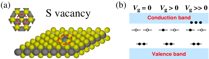
In experimental STM studies on monolayer TMDs, atomic monovacancies have been found to be among the dominating sources of intrinsic lattice disorder Zhou et al. (2013); Lin et al. (2014); Hong et al. (2015); Zhang et al. (2017); Edelberg et al. (2019); Schuler et al. (2019). Their stability and electronic structure have been studied in great detail theoretically Komsa et al. (2012); Liu et al. (2013); Noh et al. (2014); Komsa et al. (2014); Carvalho and Neto (2014); Komsa and Krasheninnikov (2015); Haldar et al. (2015); Pandey et al. (2016); Khan et al. (2017), demonstrating that they often introduce in-gap states, as illustrated in Fig. 1 for a S vacancy in MoS2, which are localized at the vacancy site. In-gap states play a crucial role in the transport properties of 2D TMDs as they can trap charges. At low gate-induced doping levels, electrons become trapped in empty in-gap states and variable-range hopping between the defect sites dominates the transport Ghatak et al. (2011); Qiu et al. (2013); Yu et al. (2014); Chen et al. (2014); Ponomarev et al. (2018). With increasing doping, the material becomes -type with free carriers in the conduction band. At this point, a transition from the insulating state with thermally-activated hopping transport to a metallic conduction regime with a conductivity (resistivity) that decreases (increases) with increasing temperature takes place Ghatak et al. (2011); Baugher et al. (2013); Radisavljevic and Kis (2013); Schmidt et al. (2014); Yu et al. (2014); Cui et al. (2015b); Yu et al. (2016, 2017). Usually, metallic behavior is attributed to electron-phonon scattering, but this is suppressed at low temperature and disorder scattering by, e.g., atomic vacancies becomes the mobility-limiting factor Yu et al. (2014); Chu et al. (2014); Schmidt et al. (2014); Cui et al. (2015a); Schmidt et al. (2016).
In this work, we provide an in-depth study of the effect of atomic vacancies on carrier scattering and transport in - and -type 2D MoS2. Conventionally, atomic vacancies in 2D TMDs are treated as neutral point defects (see, e.g., Ref. Yuan et al., 2014) which act as short-range scatterers. However, in the presence of vacancy-induced in-gap states, vacancies may acquire a dual character due to charging of the vacancy site, and should be treated as combined short-range and long-range Coulomb (i.e., charged impurity) scatterers.
The situation for an S vacancy in 2D MoS2 Komsa et al. (2012); Liu et al. (2013); Noh et al. (2014); Komsa et al. (2014); Carvalho and Neto (2014); Komsa and Krasheninnikov (2015); Haldar et al. (2015); Pandey et al. (2016); Khan et al. (2017) is illustrated in Fig. 1 where the vacancy gives rise to three in-gap states. The lowest state is doubly occupied in the undoped, charge neutral material (), and hence behaves as a donor state which traps holes in -doped materials. On the other hand, the upper states are empty and behave as deep single-electron acceptors which trap electrons in -doped () samples Liu et al. (2013); Noh et al. (2014); Qiu et al. (2013); Yu et al. (2014) (doubly charged vacancy sites are expected to be prohibited by a large onsite Coulomb repulsion energy). Thus, S vacancies are expected to acquire a net charge in - or -doped MoS2 (positive and negative, respectively) due to charging of the in-gap states. The same holds for Mo vacancies in MoS2 (see, e.g., Ref. Haldar et al., 2015). However, while vacancies in 2D TMDs, in general, seem to introduce empty in-gap states, occupied states above the valence-band edge are not always present Haldar et al. (2015); Li et al. (2016). In the latter case, the vacancy will remain neutral in the -doped material.
Based on the -matrix formalism Rammer (1998); Bruus and Flensberg (2004), we here demonstrate that the scattering amplitude for the short-range component of the scattering potential is strongly renormalized with respect to its value in the Born approximation. For charged vacancies, this renders the short-range potential irrelevant in comparison to the Coulomb contribution to the scattering potential, and effectively reduces the vacancies to charged impurities.
The dominance of Coulomb disorder scattering gives rise to a strong temperature and density dependence of the mobility which stems from the temperature dependent screening of the Coulomb potential. In the degenerate low-temperature () regime, Coulomb disorder resembles short-range disorder due to the efficient carrier screening in 2D TMDs, and yields a behavior. At the crossover to the nondegenerate () regime, the screening efficiency is strongly reduced due to the temperature dependence of the 2D screening function, and the experimentally observed metallic behavior with a mobility that decreases with increasing temperature and increases with the carrier density prevails. While this behavior is inherent to any 2D semiconductor systems at the quantum-classical crossover () between the degenerate and nondegenerate regimes Das Sarma and Hwang (2015), the temperature and density interval where the crossover takes place is highly dependent on material parameters (spin and valley degeneracy, effective mass). For typical carrier densities (– cm-2) in 2D TMDs, the Fermi temperature falls in the range , thus placing the quantum-classical crossover in an easily accessible temperature range where phonon scattering is weak Kaasbjerg et al. (2012, 2013).
In 2D TMDs where the vacancies remain neutral in the -doped material, the mobility is demonstrated to be significantly higher and shows much weaker temperature dependence as well as a qualitatively different density dependence with a mobility that decreases with the carrier density. This behavior is inherent to atomic-vacancy limited transport in 2D TMDs with charge-neutral vacancies.
Our findings are of high relevance for the understanding of the microscopic factors governing the mobility, magneto and quantum transport in 2D TMDs Ovchinnikov et al. (2014); Cui et al. (2015a); Schmidt et al. (2016); Mak et al. (2014); Fallahazad et al. (2016); Cui et al. (2017); Pisoni et al. (2018a); Gustafsson et al. (2018); Larentis et al. (2018); Pisoni et al. (2018b); Chu et al. (2019).
II Low-energy Hamiltonian and Boltzmann transport theory
In 2D TMDs, the valence and conduction band valleys illustrated in Fig. 2, can be described by the effective low-energy Hamiltonian Xiao et al. (2012)
| (1) |
where is the lattice parameter, a hopping parameter, is the valley index, is the band gap, ( meV in 2D MoS2) is the spin-orbit (SO) induced spin splitting at the top of the valence band Zhu et al. (2011), and , and , are the identity () and Pauli matrices ) in the symmetry-adapted orbital basis, valley and spin, respectively. The orbital basis is spanned by the -orbitals and .
In the continuum description of Eq. (1), the wave function can be expressed as (suppressing the spin index for brevity) where is the sample area and the valence () and conduction () band eigenspinors are dominated by, respectively, and near the band edges Shan et al. (2013). In this energy range, the bands are parabolic , where is the band-edge position (the spin dependence is shown in Fig. 2). The small SO splitting of 2–3 meV in the conduction band of MoS2 Kormányos et al. (2013); Kośmider et al. (2013) is here neglected and spin degeneracy is assumed. For the effective masses, we use our calculated DFT values, and for 2D MoS2 cal , which are in good agreement with previously reported values Cheiwchanchamnangij and Lambrecht (2012); Kaasbjerg et al. (2012); Kormányos et al. (2013).
II.1 Disorder-limited transport
In Boltzmann transport theory, the carrier mobility , where is the conductivity, limited by elastic disorder scattering can be expressed as , where is the effective mass and is the total energy-dependent momentum relaxation time given by the sum over contributions from different types of disorder, . The brackets denote the energy-weighted average defined as
| (2) |
Here, is the two-dimensional carrier density, is the constant density of states in 2D, and are the spin ( for ) and valley degeneracy, respectively, is the equilibrium Fermi-Dirac distribution function, and is the chemical potential. For a degenerate electron gas, scattering is restricted to a thin shell of width around the Fermi level and .
For random disorder, the relaxation time due to intra () and intervalley () scattering off defects of type is in the Born approximation given by
| (3) |
where is the disorder density, is the matrix element (in units of ) of the defect scattering potential with respect to the electronic states in band and with wave vectors , and is the scattering angle.
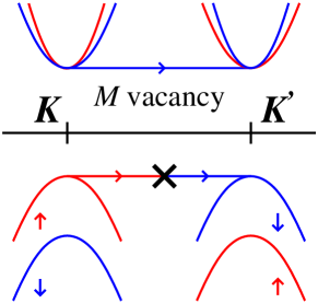
Here, we omit spin-flip scattering and limit the discussion to spin-conserving scattering off nonmagnetic defects, . Due to the orthogonality of the valence-band orbitals, , the valence-band intervalley matrix element is in general suppressed Shan et al. (2013). Recently, we have demonstrated a stricter symmetry-induced selection rule for defects with symmetry which applies to the intervalley matrix element in both the valence and conduction bands Kaasbjerg et al. (2017) (see also Sec. II.2.1 below). As a consequence, intervalley scattering in 2D TMDs is only allowed in the conduction band for metal-centered defects as illustrated in Fig. 2.
Conventionally, point defects such as atomic vacancies are treated as short-range scatterers described by a -function scattering potential in real space, where is a band-dependent disorder strength. In this case, the matrix element is simply given by
| (4) |
where the valley dependence accounts for the above-mentioned selection rules. In the Born approximation, this yields a momentum relaxation time, , and mobility, , which are independent on the carrier energy and carrier density, respectively. For atomic vacancies in 2D TMDs this approach may break down for two reasons.
First of all, as discussed in the introduction, charging of the vacancy sites in the presence of in-gap states gives rise to two distinct contributions to the scattering potential given, respectively, by (i) a short-range potential () associated with the atomic-scale point defect created by the vacancy, and (ii) a long-range Coulomb potential () due to the charged vacancy site. Here, we assume that the relaxation time for charged vacancies can be obtained as
| (5) |
where the two relaxation times on the right-hand side account for the above-mentioned contributions to the scattering potential.
Secondly, the Born approximation only applies to weak short-range disorder, i.e. when is small (see discussion in Sec. II.2.1), and may break down for vacancies. For disorder of arbitrary strength, the bare matrix element in Eq. (II.1) must be replaced with the matrix, i.e. Bruus and Flensberg (2004). The matrix solves the single-defect problem exactly by taking into account multiple scattering off the individual defects, and is hence exact for dilute disorder, i.e. where is the unit-cell area.
In the following subsections, we analyse the scattering properties of atomic vacancies (Mo and S) in 2D TMDs.
II.2 Short-range potential:
Short-range disorder due to atomic point defects often act as strong scattering centers, and must be treated with the -matrix formalism which describes multiple scattering off the same defect to infinite order in the scattering potential Bruus and Flensberg (2004). Here, we combine atomistic calculations with an analytic approach to get a realistic description of the matrix scattering rate.
II.2.1 Low-energy -matrix model
For a general defect characterized by the matrix element of its scattering potential between the Bloch states with wave vectors st Brillouin zone (BZ), the matrix (for a given spin) is given by the integral equation
| (6) |
where is the bare Green’s function and the integral is over the 1st BZ.
With the bandstructure described by the low-energy model in Eq. (1), we confine the integral in (6) to the valleys, i.e. , and parametrize the defect matrix element by a band- and valley-dependent disorder strength like in Eq. (4). With this, the -matrix equation in (6) reduces to a -independent algebraic matrix equation in the valley indices,
| (7) |
where is diagonal with elements given by the -integrated valley GF, , and the diagonal (off-diagonal) elements of correspond to intravalley (intervalley) couplings.
In a recent work Kaasbjerg et al. (2017), we have shown that the intervalley coupling due to defects in 2D TMDs with symmetry is suppressed by a symmetry-induced selection rule, except for -centered defects where intervalley coupling is possible in the conduction band as illustrated in Fig. 2. As the intra- and intervalley matrix elements for vacancies are comparable Kaasbjerg et al. (2017), a single disorder strength can therefore be considered for both and vacancies. The defect potential can hence be written
| (11) |
which captures the defect and band dependent suppression of the intervalley coupling described above.
With the form of the defect potential in (11), the matrix in (7) simplifies considerably. For the two cases in (11), we get
| (15) |
where
| (16) |
is the band and valley dependent matrix with denoting a valley multiplication factor given by the number of inequivalent valleys coupled by the defect type , i.e. and otherwise. For the parabolic bands in the valleys, the -integrated Green’s function for becomes
| (17) |
where is the density of states excluding spin and valley degeneracy, is the valley (and spin) dependent band extrema, and is an ultraviolet cut-off to be determined below. Note that due to the neglected spin-orbit splitting in the conduction band, i.e. , the elements of the matrix in the upper equation in Eq. (15) become independent on the valley index.
Via the optical theorem Rammer (1998); Bruus and Flensberg (2004), in Eq. (16) can be identified as the scattering amplitude in the -matrix approximation. Together with Eq. (17), the formal condition for disorder to be weak (strong) thus becomes (). In monolayer MoS2 eV-1Å-2, implying that eV Å2 corresponds to strong/weak disorder. For weak disorder, the Born approximation for the scattering amplitude, , is recovered, whereas the matrix becomes independent on the disorder potential, , for strong disorder in the unitary limit, . In the intermediate regime, the matrix should also be considered as it gives rise to a nonnegligible renormalization of the Born scattering amplitude.
The -matrix renormalization of the Born scattering amplitude manifests itself in an inherent energy dependence of the scattering rate. For the -matrix in Eq. (16), the inverse momentum relaxation time in Eq. (II.1) becomes,
| (18) |
which for the constant defect potentials considered here, is identical to the quantum scattering rate related to the imaginary part of the matrix [see Eq. (19) below], and given by Eq. (II.1) with the replacement . Thus where the factor stems from the integral in Eq. (II.1).
Figure 3 shows the energy dependence of the inverse relaxation time in Eq. (18) (full lines) in terms of for parameters corresponding to Mo and S vacancies in MoS2 (see Sec. II.2.2 below). The characteristic behavior of the scattering rate which increases away from the band edge where it drops sharply, can be traced back to in (17) which diverges for due to the logarithm in its real part. This behavior is inherent to intermediate and strong short-range disorder, such as, e.g., vacancies and point defects, in 2D materials with parabolic bands, and in stark contrast to the constant relaxation time in the Born approximation, , which is recovered for weak disorder.
Also, the above is in contrast to the situation for vacancies in graphene where the scattering rate is predicted to have a nonmonotonic energy dependence due to resonance scattering off quasibound defect states in the vicinity of the Dirac point Ostrovsky et al. (2006); Stauber et al. (2007); Basko (2008); Wehling et al. (2010); Kaasbjerg .
II.2.2 Effective disorder parameters for vacancies
To determine the -matrix parameters for Mo and S vacancies which enter Eq. (16), we have used the atomistic method outlined in Refs. Kaasbjerg et al., 2017; Kaasbjerg, to calculate the matrix for atomic vacancies in 2D MoS2 based on Eq. (6) with DFT inputs for the band structure (including spin-orbit interaction) and defect matrix elements sampled in the entire BZ cal .
In order to quantify our atomistic calculations, we consider the quasiparticle scattering rate , where
| (19) |
is the lifetime broadening given by the imaginary part of the on-shell () -matrix self-energy of the disorder-averaged Green’s function Rammer (1998); Bruus and Flensberg (2004).
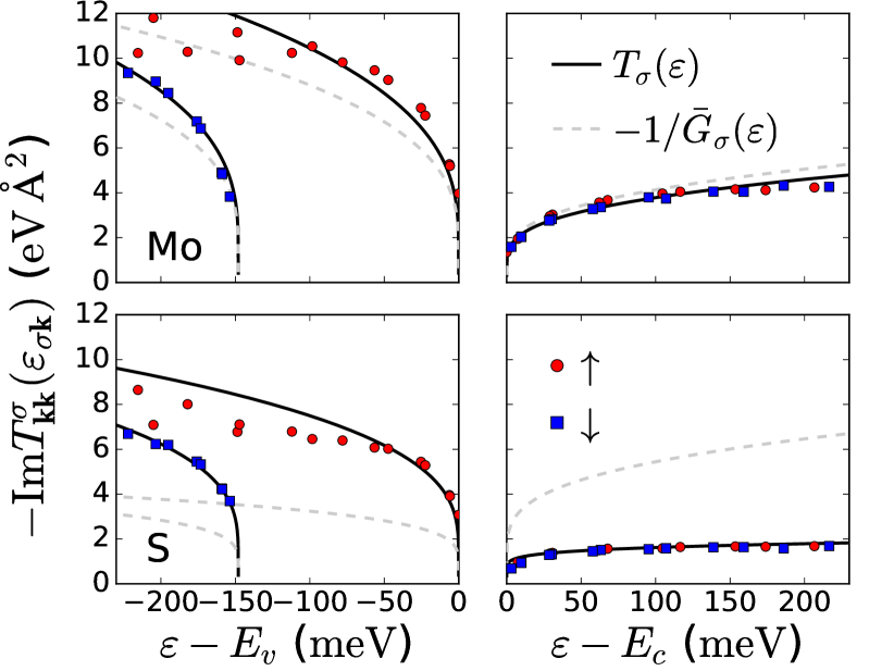
Figure 3 shows the imaginary part of the calculated on-shell matrix for Mo (top) and S (bottom) vacancies Kaasbjerg et al. (2017); Kaasbjerg as a function energy in the valley of the valence (left) and conduction (right) band. The red dots and blue squares correspond to the -matrix for the spin-orbit split spin up and down bands, respectively. In the plots for the valence band, the offset in energy between the red dots and blue squares is due to the large spin-orbit splitting between the spin up and down bands ( meV) in the valleys. In the conduction band, the small spin-orbit splitting of –3 meV is hardly discernible, and the imaginary part of the matrix is almost identical for the spin up and down bands. The -matrix results in Fig. 3 can be converted to a lifetime broadening via Eq. (19), and correspond to a broadening of the order of –0.1 meV for a disorder density of . Furthermore, the atomistic -matrix results confirm the characteristic energy dependence of the lifetime broadening, or scattering rate, predicted by Eq. (18).
| Valence band | Conduction band | |
|---|---|---|
| Mo vacancy | ||
| eV | eV | |
| S vacancy | ||
| eV | eV | |
The -matrix parameters for vacancies are obtained by fitting the analytic expression (16) to the atomistic matrix in Fig. 3 [we fit the imaginary parts to achieve an optimal description of the scattering rate, cf. Eq. (19)]. In the fitting procedure, we first fix the disorder strength to the value of the atomistic matrix elements at the points (see Refs. Kaasbjerg et al., 2017; Kaasbjerg, ), and treat the ultraviolet cutoff as a fitting parameter. This is justified as does not have an immediate physical interpretation in the low-energy -matrix model. Instead, it should be regarded as an effective parameter which compensates for approximating in Eq. (6) (i) the band structure in the full BZ with parabolic bands in the valleys, and (ii) the defect matrix element by a constant disorder strength.
The resulting fits are shown with solid lines (the dashed lines show the unitary limit) in Fig. 3, and are seen to match the atomistic calculations almost perfectly, in particular at energies near the band edges relevant for transport. The corresponding fitting parameters are summarized in Table 1.
As witnessed by Fig. 3, the matrix is highly dependent on the band. This is due to the factor in front of the real part of in Eq. (17), which even for an electron-hole symmetric bandstructure gives rise to different scattering rates for electrons and holes [cf. Eq. (18)]. For (the reverse holds for ), this leads to a hole scattering rate which is larger than the electron scattering rate as seen in Fig. 3. For the same reason, the electron and holes rates are, respectively, larger and smaller than the rate for unitary scattering.
Finally, we note that the -matrix results in Fig. (3) correspond to a significant renormalization of the Born scattering amplitude given by the bare disorder strengths in Tab. 1. From the numbers in Fig. 3, the -matrix scattering amplitudes are found to be up to an order of magnitude smaller than the Born scattering amplitudes. The renormalization is most pronounced for Mo vacancies which are strong (almost unitary) scatterers, and still noticeable for the weaker S vacancies. As the scattering rate depends on the square of the scattering amplitude, the Born approximation therefore severely overestimates the scattering rate.
To summarize, the strong -matrix renormalization of the Born scattering amplitude results in (i) the characteristic energy dependence of the scattering rates in Fig. 3, as well as (ii) a significant reduction of the scattering rate relative to the Born result. These findings points to a concomitant breakdown of the Born approximation for atomic-vacancy scattering in 2D TMDs.
II.3 Long-range Coulomb potential:
The relaxation time in Eq. (5) due to trapped charges in the in-gap states is governed by a long-range Coulomb potential. Due to the localized nature of the in-gap states, this can be approximated by the screened Coulomb potential from a point charge located at the vacancy site, and the matrix element becomes
| (20) |
where is the static dielectric function of the 2D material which includes both intra and interband screening as discussed in further detail in Sec. II.3.1 below.
For scattering off the long-range Coulomb potential, we use the Born approximation which is justified due to the screening of the Coulomb potential Ong and Fischetti (2013); Das Sarma and Hwang (2013); Ma and Jena (2014); Das Sarma and Hwang (2014, 2015). For a degenerate 2DEG, the dielectric function is given by , , where is the Thomas-Fermi (TF) wave vector and is a background dielectric constant. In 2D TMDs, , where is the lattice constant, implying that carrier screening is very efficient. This changes qualitatively the dependence of the unscreened Coulomb potential, with the screened Coulomb matrix element in (20) becoming
| (21) |
which is independent on , and thus resembles short-range disorder with an effective disorder strength . For , the screening efficiency is reduced and the unscreened potential is recovered. In 2D MoS2, the effective disorder strengths in the valence and conduction bands are Å2 and Å2, respectively.
In passing, we note that scattering off an unscreened 2D Coulomb potential was studied with a partial-wave analysis (which is equivalent to a -matrix treatment) in Ref. g. Lin, 1997. However, as it has been shown in numerous works Ong and Fischetti (2013); Das Sarma and Hwang (2013); Ma and Jena (2014); Das Sarma and Hwang (2014, 2015), it is important to take into account screening for a correct description of the density and temperature dependence of the low-temperature conductivities in 2D systems.
II.3.1 Dielectric function
The long-wavelength dielectric function of a doped 2D semiconductor has two contributions: the first is due to the gate-induced extrinsic carriers which is normally accounted for in transport studies, and the second from the intrinsic screening associated with virtual electron-hole (eh) pair excitation between the valence and conduction bands. Contrary to 3D bulk systems where the latter is well described by the dielectric constant of the material, intrinsic screening in 2D semiconductors is strongly dependent Cudazzo et al. (2011); Qiu et al. (2016).
The total dielectric function thus becomes
| (22) |
where is the 2D Fourier transform of the Coulomb interaction and () is the polarizability due to intraband (interband) eh-pair processes involving extrinsic (intrinsic) carriers. Dielectric screening from the environment is included with the replacements and , where is an effective background dielectric constant for encapsulation in -BN Ma and Jena (2014).
The screening from the extrinsic carriers in the valence/conduction band is described with finite-temperature RPA theory where the static polarizability at finite temperatures is given by Maldague (1978); Ando et al. (1982)
| (23) |
Here, is the zero-temperature polarizability and the integral is evaluated following Ref. Flensberg and Yu-Kuang Hu, 1995. For a degenerate 2DEG, Eq. (23) yields the above-mentioned TF result for the extrinsic screening. In the nondegenerate regime, extrinsic carrier screening is described by Debye-Hückel theory and is strongly reduced. Thus, the strength of the Coulomb potential increases dramatically, and the transport is expected to become dominated by Coulomb-disorder scattering at low carrier density and high temperature.
For the intrinsic screening due to interband eh-pair excitations between the valence and conduction bands, we use the dielectric function Cudazzo et al. (2011); Qiu et al. (2016)
| (24) |
which is valid in the long-wavelength limit and where is given by the interband polarizability , and Å for MoS2 Latini et al. (2015); Olsen et al. (2016). Note that the intrinsic screening vanishes, , for in 2D semiconductors. As it originates from eh-pair excitations between bands separated by a large band gap, the intrinsic screening is not expected to depend on temperature.
II.3.2 Extrinsic vs intrinsic screening
The dielectric function in Eq. (22) is similar to the one in gated graphene Hwang and Das Sarma (2007). However, due the sizeable band gaps in 2D TMDs, intrinsic screening is much weaker than in graphene, and the long-wavelength dielectric function is dominated by intraband processes involving extrinsic carriers.
Already from the dependence of the polarizabilities it is clear that extrinsic screening dominates the total dielectric function in Eq. (22) in the long-wavelength limit. For a degenerate carrier distribution, the wave vector at which the two screening mechanisms contribute equally to the total dielectric function can be estimated by comparing the products of the Coulomb interaction and the polarizabilities,
| (25) |
For monolayer MoS2, we estimate based on the conduction-band TF wave vector. Thus, extrinsic screening dominates at temperatures where the scattering wave vector is limited by , whereas at (i) high temperatures where extrinsic carrier screening is reduced, and (ii) high carrier densities where becomes appreciable compared to , intrinsic screening becomes important.
III Results
In the following, we present our results for the density, , and temperature, , dependencies of the mobility limited by atomic vacancies. As the inverse relaxation time scales directly with the disorder density, we restrict here the discussion to cm-2 which corresponds to a dilute concentration () of defects.
From our considerations in the previous section, we anticipate a density scaling of the mobility with (i) if the short-range potential dominates as the scattering rate increases with the electron and hole energies [cf. Fig. 3 and Eq. (18)], and (ii) if the Coulomb potential dominates Das Sarma and Hwang (2014, 2013).
III.1 Charged vacancies: Coulomb-disorder dominated transport
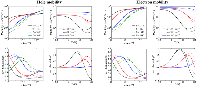
In Fig. 4 we show the density and temperature dependence of the mobility limited by charged vacancies. As we explain below, the results for charged Mo and S vacancies are almost identical, hence only the results for S vacancies are shown. The scaling exponents and are shown in the bottom panels. To emphasize effect of the intrinsic interband screening, we show the results both with (full lines) and without (dashed lines; ) intrinsic screening, and the dots indicate the densities and temperatures where the Fermi temperature is equal to the actual temperature, , and hence mark the quantum-classical crossover between the degenerate () and nondegenerate () regimes.
Overall, the mobilities limited by charged S vacancies show a strong density and temperature dependence with and , except at high temperatures and low densities where . These observations indicate that the vacancy-independent Coulomb potential scattering dominates the inverse relaxation time for charged vacancies, thus resulting in almost identical mobilities for charged Mo and S vacancies. Based on the observations regarding the energy dependence of the relaxation time in Eq. 18, a density scaling would have been expected if the short-range potential was dominating.
This is also consistent with the observed strong temperature dependence of the mobility which stems from the temperature-dependent screening of the Coulomb potential. Moving from the quantum-classical crossover into the nondegenerate low-density/high-temperature regimes, the strength of the Coulomb potential increases dramatically due to a strong reduction in the efficiency of extrinsic carrier screening. In turn, this leads to a pronounced reduction of the mobility of up to two orders of magnitude.
The effect of intrinsic screening on the Coulomb potential is evident at high temperatures where it becomes comparable to extrinsic screening. Here, it gives rise to an unusual upturn in the mobility with increasing temperature (compare full and dashed lines). Also, at high densities the mobilities show a pronounced upturn with increasing density. This is again due to the intrinsic screening which becomes stronger with increasing density () due to its linear dependence in (II.3.1). Overall, the differences between the full and dashed lines show that intrinsic screening gives rise to a significant boost of the mobility in the nondegenerate regime and for high densities in the degenerate regime.
Finally, we note that the hole mobilities are in general lower than the electron mobilities in the degenerate regime. This can be attributed to the lack of spin degeneracy in the valence band which results in a weaker screening of Coulomb scattering for holes (cf. Sec. II.3).
The density and temperature range where the pronounced screening-induced change in the mobilities in Fig. 4 takes place, is summarized in the transport diagram shown for the S-vacancy limited conductivity in -type MoS2 in Fig. 5. The diagram shows the conductivity (here ) in the plane and the black dashed line indicates the quantum-classical crossover at . As is evident, the crossover takes place at experimentally easily accessible densities and temperatures.
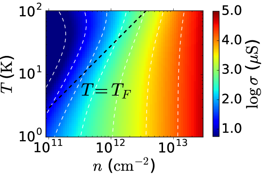
The quantum-classical crossover is clearly visible in the conductivity data. In the degenerate high-density regime (), the conductivity scales as and is almost independent on temperature due to the effective short-range nature of the Coulomb potential in Eq. (21) caused by carrier screening. At , the conductivity acquires a stronger density and temperature dependence due to the reduced screening of the Coulomb potential.
III.2 Neutral vacancies: Short-range disorder limited transport
In this section, we consider the situation where the vacancies remain neutral in doped samples. This is expected to occur in 2D TMDs where vacancies do not introduce occupied in-gap states (e.g., vacancies in W Haldar et al. (2015); Li et al. (2016)), implying that the vacancy will remain overall neutral in -doped samples and only the short-range contribution to the relaxation time in Eq. (5) remains.
To demonstrate the impact on the hole mobility in TMDs where the above-mentioned situation is realized, we show in Fig. 6 the hole mobility in MoS2 limited by neutral S vacancies at different temperatures. The dashed line shows the zero-temperature mobility with the relaxation time obtained from Eq. (18). As the semiconducting 2D TMDs have similar valence band structure, only minor quantitative changes are expected for hole mobility limited by neutral and vacancies in other TMDs.
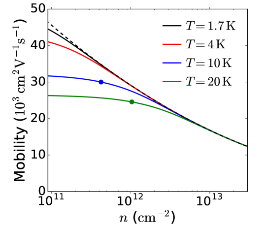
First of all, we note that the mobilities are more than an order of magnitude higher than the ones in Fig. 4 limited by charged vacancies, except at the highest carrier densities where they become comparable. The fact that the mobilities are higher for neutral vacancies, is not surprising because the Coulomb potential completely dominates the short-range potential for scattering off charged vacancies. As we had anticipated from the scattering rates deduced from Fig. 3, the mobilities in Fig. 6 limited alone by the short-range potential due to neutral vacancies, decrease with increasing carrier density. This rather unusual density dependence of the mobility is a direct consequence of the -matrix induced renormalization of the scattering amplitude. At low densities, the decreasing temperature dependence of the mobility stems from the energy average of the relaxation time in Eq. (2), which with increasing temperature probes the increasing energy dependence of the scattering rate at higher energies. The resulting reduction in the mobility is, however, much smaller than the sceening-related reduction observed for charged vacancies.
The qualitative difference between the screening-induced and -matrix induced density and temperature dependencies of the mobility emerges clearly from the transport diagrams for charged and neutral vacancies in Figs. 5 and 7, respectively. While in the latter case, the conductivity scales roughly as on both sides of the quantum-classical crossover, the screening-induced density dependence of the scattering rate in the former case results in a stronger behavior in the nondegenerate regime at .
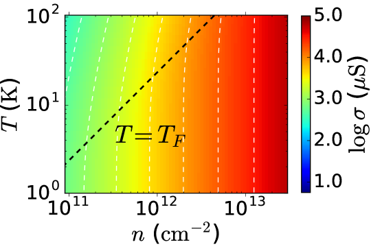
These qualitative differences in the transport characteristics allow to clearly distinguish Coulomb-disorder limited transport from short-range limited transport due to, e.g., charged and neutral vacancies, respectively.
IV Discussion
Reported experimental low-temperature mobilities in 2D TMDs have thus far been rather low Baugher et al. (2013); Radisavljevic and Kis (2013); Schmidt et al. (2014); Yu et al. (2014); Cui et al. (2015a, b); Yu et al. (2016), and have only recently exceeded 1000 cmVs-1 Fallahazad et al. (2016); Pisoni et al. (2018a); Gustafsson et al. (2018); Larentis et al. (2018); Pisoni et al. (2018b). This is still slightly lower than our calculated mobilities limited by charged vacancies and much lower than the calculated mobilities limited by neutral vacancies. This indicates that the concentration of vacancies in experimental samples could be higher than cm-2 used here. Several reports of high concentrations of S vacancies Qiu et al. (2013); Yu et al. (2014) suggest that this is indeed a likely reason for the low experimental mobilities. Only recently have defect densities of cm-2 been demonstrated Edelberg et al. (2019). However, experimental transport properties of such high-quality TMDs have so far not been reported.
The often observed strong metallic temperature and density dependence of experimental low-temperature mobilities Baugher et al. (2013); Radisavljevic and Kis (2013); Schmidt et al. (2014); Yu et al. (2014); Cui et al. (2015a, b); Yu et al. (2016) resemble best our results for charged vacancies. This indicates that a combination short-range and Coulomb-disorder scattering is limiting the low-temperature mobility in 2D TMDs. As we here suggest, vacancies may be the source of both short-range and Coulomb disorder scattering. Hence, there is no need to introduce additional Coulomb disorder Ong and Fischetti (2013); Ma and Jena (2014) (e.g., charged impurities in the substrate) in order to account for the metallic transport behavior.
V Conclusions
In conclusion, we have studied the effect of atomic vacancies on carrier scattering and transport in - and -type monolayer MoS2. Due to the presence of both filled and empty vacancy-induced in-gap states, the vacancies can be expected to become charged in - and -doped MoS2, and thereby give rise to both short-range and Coulomb disorder scattering. The situation is similar for vacancies in many other 2D TMDs, but cases lacking filled in-gap states have been reported, implying that the vacancy remain neutral in the -doped material.
Studying the short-range scattering properties of vacancies with the -matrix formalism, we show that multiple scattering gives rise to a strong renormalization of the Born scattering amplitude, which results in a pronounced reduction as well as a characteristic energy dependence of the scattering rate. As a result, the Coulomb contribution to the scattering potential for charged vacancies by far dominates carrier scattering. This results in a strong screening-induced temperature and density dependence of the mobility in 2D TMDs hosting charged vacancies. For TMDs with neutral vacancies the mobility is significantly higher and shows an unusual behavior with a decreasing density dependence. Thus, TMDs in which vacancies remain neutral in the doped material are better candidates for high-mobility devices.
Acknowledgements.
K.K. acknowledges support from the Carlsberg Foundation and the European Union’s Horizon 2020 research and innovation program under the Marie Sklodowska-Curie Grant Agreement No. 713683 (COFUNDfellowsDTU). T.L. acknowledges partial support from NSF ECCS-1542202. The Center for Nanostructured Graphene (CNG) is sponsored by the Danish National Research Foundation, Project DNRF103.’
References
- Mak et al. (2010) K. F. Mak, C. Lee, J. Hone, J. Shan, and T. F. Heinz, “Atomically thin MoS2: A new direct-gap semiconductor,” Phys. Rev. Lett. 105, 136805 (2010).
- Radisavljevic et al. (2011) B. Radisavljevic, A. Radenovic, J. Brivio, V. Giacometti, and A. Kis, “Single-layer MoS2 transistors,” Nature Nano. 6, 147 (2011).
- Korn et al. (2011) T. Korn, S. Heydrich, M. Hirmer, J. Schmutzler, and C. Schüller, “Low-temperature photocarrier dynamics in monolayer MoS2,” Appl. Phys. Lett. 99, 102109 (2011).
- Avouris et al. (2017) Phaedon Avouris, Tony F Heinz, and Tony Low, 2D Materials (Cambridge University Press, 2017).
- Xiao et al. (2012) D. Xiao, G.-B. Liu, W. Feng, X. Xu, and W. Yao, “Coupled spin and valley physics in monolayers of MoS2 and other group-VI dichalcogenides,” Phys. Rev. Lett. 108, 196802 (2012).
- Yao et al. (2014) X. Xu W. Yao, D. Xiao, and T. F. Heinz, “Spin and pseudospins in layered transition metal dichalcogenides,” Nature Phys. 10, 343 (2014).
- Kormányos et al. (2014) A. Kormányos, V. Zólyomi, N. D. Drummond, and G. Burkard, “Spin-orbit coupling, quantum dots, and qubits in monolayer transition metal dichalcogenides,” Phys. Rev. X 4, 011034 (2014).
- Liu et al. (2014) G.-B. Liu, H. Pang, Y. Yao, and W. Yao, “Intervalley coupling by quantum dot confinement potentials in monolayer transition metal dichalcogenides,” New J. Phys. 16, 105011 (2014).
- Wu et al. (2016) Y. Wu, Q. Tong, G.-B. Liu, H. Yu, and W. Yao, “Spin-valley qubit in nanostructures of monolayer semiconductors: Optical control and hyperfine interaction,” Phys. Rev. B 93, 045313 (2016).
- Pawlowski et al. (2018) J. Pawlowski, D. Zebrowski, and S. Bednarek, “Valley qubit in gated MoS2 monolayer quantum dot,” Phys. Rev. B 97, 155412 (2018).
- Pisoni et al. (2018a) R. Pisoni, Z. Lei, P. Back, M. Eich, H. Overweg, Y. Lee, K. Watanabe, T. Taniguchi, T. Ihn, and K. Ensslin, “Gate-tunable quantum dot in a high quality single layer MoS2 van der Waals heterostructure,” Appl. Phys. Lett. 112, 123101 (2018a).
- Rhodes et al. (2019) D. Rhodes, S. H. Chae, R. Ribeiro-Palau, and J. Hone, “Disorder in van der Waals heterostructures of 2D materials,” Nature Mat. 18, 541 (2019).
- Radisavljevic and Kis (2013) B. Radisavljevic and A. Kis, “Mobility engineering and a metal-insulator transition in monolayer MoS2,” Nature Mat. 12, 815 (2013).
- Baugher et al. (2013) B. W. H. Baugher, H. O. H. Churchill, Y. Yang, and P. Jarillo-Herrero, “Intrinsic electronic transport properties of high-quality monolayer and bilayer MoS2,” Nano. Lett. 13, 4212 (2013).
- Zhu et al. (2014) W. Zhu, T. Low, Y.-H. Lee, H. Wang, D. B. Farmer, J. Kong, F. Xia, and P. Avouris, “Electronic transport and device prospects of monolayer molybdenum disulphide grown by chemical vapour deposition,” Nature Commun. 5, 3087 (2014).
- Yu et al. (2014) Z. Yu, Y. Pan, Y. Shen, Z. Wang, Z.-Y. Ong, T. Xu, R. Xin, L. Pan, B. Wang, L. Sun, J. Wang, G. Zhang, Y. W. Zhang, Y. Shi, and X. Wang, “Towards intrinsic charge transport in monolayer molybdenum disulfide by defect and interface engineering,” Nature Commun. 5, 5290 (2014).
- Schmidt et al. (2014) H. Schmidt, S. Wang, L. Chu, M. Toh, R. Kumar, W. Zhao, A. H. Castro Neto, J. Martin, S. Adam, B. Özyilmaz, and G. Eda, “Transport properties of monolayer MoS2 grown by chemical vapor deposition,” Nano. Lett. 14, 1909 (2014).
- Chu et al. (2014) L. Chu, H. Schmidt, J. Pu, S. Wang, B. Özyilmaz, T. Takenobu, and G. Eda, “Charge transport in ion-gated mono-, bi-, and trilayer MoS2 field effect transistors,” Scientific Reports 4, 7293 (2014).
- Cui et al. (2015a) X. Cui, G.-H. Lee, Y. Duck Kim, G. Arefe, P. Y. Huang, C.-H. Lee, D. A. Chenet, X. Zhang, L. Wang, F. Ye, F. Pizzocchero, B. S. Jessen, K. Watanabe, T. Taniguchi, D. A. Muller, T. Low, P. Kim, and J. Hone, “Multi-terminal transport measurements of MoS2 using a van der Waals heterostructure device platform,” Nature Nano. 10, 534 (2015a).
- Schmidt et al. (2016) H. Schmidt, I. Yudhistira, L. Chu, A. H. Castro Neto, B. Özyilmaz, S. Adam, and G. Eda, “Quantum transport and observation of Dyakonov-Perel spin-orbit scattering in monolayer MoS2,” Phys. Rev. Lett. 116, 046803 (2016).
- Cui et al. (2017) X. Cui, E.-M. Shih, L. A. Jauregui, S. H. Chae, Y. D. Kim, B. Li, D. Seo, K. Pistunova, J. Yin, J.-H. Park, H.-J. Choi, Y. H. Lee, K. Watanabe, T. Taniguchi, P. Kim, C. R. Dean, and J. C. Hone, “Low-temperature ohmic contact to monolayer MoS2 by van der Waals bonded Co/-BN electrodes,” Nano. Lett. 17, 4781 (2017).
- Fallahazad et al. (2016) B. Fallahazad, H. C. P. Movva, K. Kim, S. Larentis, T. Taniguchi, K. Watanabe, S. K. Banerjee, and E. Tutuc, “Shubnikov-de Haas oscillations of high-mobility holes in monolayer and bilayer WSe2: Landau level degeneracy, effective mass, and negative compressibility,” Phys. Rev. Lett. 116, 086601 (2016).
- Gustafsson et al. (2018) M. V. Gustafsson, M. Yankowitz, C. Forsythe, D. Rhodes, K. Watanabe, T. Taniguchi, J. Hone, X. Zhu, and C. R. Dean, “Ambipolar Landau levels and strong band-selective carrier interactions in monolayer WSe2,” Nature Mat. 17, 411 (2018).
- Larentis et al. (2018) S. Larentis, H. C. P. Movva, B. Fallahazad, K. Kim, A. Behroozi, T. Taniguchi, K. Watanabe, S. K. Banerjee, and E. Tutuc, “Large effective mass and interaction-enhanced Zeeman splitting of -valley electrons in MoSe2,” Phys. Rev. B 97, 201407(R) (2018).
- Pisoni et al. (2018b) R. Pisoni, A. Kormányos, M. Brooks, Z. Lei, P. Back, M. Eich, H. Overweg, Y. Lee, P. Rickhaus, K. Watanabe, T. Taniguchi, A. Imamoglu, G. Burkard, T. Ihn, and K. Ensslin, “Interactions and magnetotransport through spin-valley coupled Landau levels in monolayer MoS2,” Phys. Rev. Lett. 121, 247701 (2018b).
- Kaasbjerg et al. (2012) K. Kaasbjerg, K. S. Thygesen, and K. W. Jacobsen, “Phonon-limited mobility in MoS2 from first principles,” Phys. Rev. B 85, 115317 (2012).
- Kaasbjerg et al. (2013) K. Kaasbjerg, K. S. Thygesen, and A.-P. Jauho, “Acoustic phonon-limited mobility in two-dimensional MoS2: Deformation potential and piezoelectric scattering from first principles,” Phys. Rev. B 87, 235312 (2013).
- Song and Dery (2013) Y. Song and H. Dery, “Transport theory of monolayer transition-metal dichalcogenides through symmetry,” Phys. Rev. Lett. 111, 026601 (2013).
- Jin et al. (2014) Z Jin, X. Li, J. T. Mullen, and K. W. Kim, “Intrinsic transport properties of electrons and holes in monolayer transition-metal dichalcogenides,” Phys. Rev. B 90, 045422 (2014).
- Ong and Fischetti (2013) Z.-Y. Ong and M. V. Fischetti, “Mobility enhancement and temperature dependence in top-gated single-layer MoS2,” Phys. Rev. B 88, 165316 (2013).
- Ma and Jena (2014) N. Ma and D. Jena, “Charge scattering and mobility in atomically thin semiconductors,” Phys. Rev. X 4, 011043 (2014).
- Ghorbani-Asl et al. (2013) M. Ghorbani-Asl, A. N. Enyashin, A. Kuc, G. Seifert, and T. Heine, “Defect-induced conductivity anisotropy in MoS2 monolayers,” Phys. Rev. B 88, 245440 (2013).
- Yuan et al. (2014) S. Yuan, R. Roldán, M. I. Katsnelson, and F. Guinea, “Effect of point defects on the optical and transport properties of MoS2 and WS2,” Phys. Rev. B 90, 041402(R) (2014).
- Olsen and Souza (2015) T. Olsen and I. Souza, “Valley Hall effect in disordered monolayer MoS2 from first principles,” Phys. Rev. B 92, 125146 (2015).
- Lu et al. (2013) H.-Z. Lu, W. Yao, D. Xiao, and S.-Q. Shen, “Intervalley scattering and localization behaviors of spin-valley coupled dirac fermions,” Phys. Rev. Lett. 110, 016806 (2013).
- Shan et al. (2013) W.-Y. Shan, H.-Z. Lu, and D. Xiao, “Spin Hall effect in spin-valley coupled monolayers of transition metal dichalcogenides,” Phys. Rev. B 88, 125301 (2013).
- Cazalilla et al. (2014) M. A. Cazalilla, H. Ochoa, and F. Guinea, “Quantum spin Hall effect in two-dimensional crystals of transition-metal dichalcogenides,” Phys. Rev. Lett. 113, 077201 (2014).
- Ochoa et al. (2014) H. Ochoa, F. Finocchiaro, F. Guinea, and V. I. Fal’ko, “Spin-valley relaxation and quantum transport regimes in two-dimensional transition-metal dichalcogenides,” Phys. Rev. B 90, 235429 (2014).
- Tahir et al. (2016) M. Tahir, P. Vasilopoulos, and F. M. Peeters, “Quantum magnetotransport properties of a MoS2 monolayer,” Phys. Rev. B 93, 035406 (2016).
- Kormányos et al. (2015) A. Kormányos, P. Rakyta, and G. Burkard, “Landau levels and Shubnikov-de Haas oscillations in monolayer transition metal dichalcogenide semiconductors,” New J. Phys. 17, 103006 (2015).
- Ilić et al. (2019) S. Ilić, J. S. Meyer, and M. Houzet, “Weak localization in transition metal dichalcogenide monolayers and their heterostructures with graphene,” Phys. Rev. B 99, 205407 (2019).
- Kaasbjerg et al. (2017) K. Kaasbjerg, J. H. J. Martiny, T. Low, and A.-P. Jauho, “Symmetry-forbidden intervalley scattering by atomic defects in monolayer transition-metal dichalcogenides,” Phys. Rev. B 96, 241411(R) (2017).
- Zhou et al. (2013) W. Zhou, X. Zou, S. Najmaei, Z. Liu, Y. Shi, J. Kong, J. Lou, P. M. Ajayan, B. I. Yakobson, and J.-C. Idrobo, “Intrinsic structural defects in monolayer molybdenum disulfide,” Nano. Lett. 13, 2615 (2013).
- Lin et al. (2014) Y.-C. Lin, T. Björkman, H.-P. Komsa, P.-Y. Teng, C.-H. Yeh, F.-S. Huang, K.-H. Lin, J. Jadczak, Y.-S. Huang, P.-W. Chiu, A. V. Krasheninnikov, and K. Suenaga, “Three-fold rotational defects in two-dimensional transition metal dichalcogenides,” Nature Commun. 6, 6736 (2014).
- Hong et al. (2015) J. Hong, Z. Hu, M. Probert, K. Li, D. Lv, X. Yang, L. Gu, N. Mao, Q. Feng, L. Xie, J. Zhang, D. Wu, Z. Zhang, C. Jin, W. Ji, X. Zhang, J. Yuan, and Z. Zhang, “Exploring atomic defects in molybdenum disulphide monolayers,” Nature Commun. 6, 6293 (2015).
- Zhang et al. (2017) S. Zhang, C.-G. Wang, M.-Y. Li, D. Huang, L.-J. Li, W. Ji, and S. Wu, “Defect structure of localized excitons in a WSe2 monolayer,” Phys. Rev. Lett. 119, 046101 (2017).
- Edelberg et al. (2019) D. Edelberg, D. Rhodes, A. Kerelsky, B. Kim, J. Wang, A. Zangiabadi, C. Kim, A. Abhinandan, J. Ardelean, M. Scully, D. Scullion, L. Embon, R. Zu, Elton J. G. Santos, L. Balicas, C. Marianetti, K. Barmak, X.-Y. Zhu, J. C. Hone, and A. N. Pasupathy, “Approaching the intrinsic limit in transition metal diselenides via point defect control,” Nano. Lett. 19, 4371 (2019).
- Schuler et al. (2019) B. Schuler, D. Y. Qiu, S. Refaely-Abramson, , C. Kastl, C. T. Chen, S. Barja, R. J. Koch, D. F. Ogletree, S. Aloni, A. M. Schwartzberg, J. B. Neaton, S. G. Louie, and A. Weber-Bargioni, “Large spin-orbit splitting of deep in-gap defect states of engineered sulfur vacancies in monolayer WS2,” Phys. Rev. Lett. 123, 076801 (2019).
- Komsa et al. (2012) H.-P. Komsa, J. Kotakoski, S. Kurasch, O. Lehtinen, U. Kaiser, and A. V. Krasheninnikov, “Two-dimensional transition metal dichalcogenides under electron irradiation: Defect production and doping,” Phys. Rev. Lett. 109, 035503 (2012).
- Liu et al. (2013) D. Liu, Y. Guo, L. Fang, and J. Robertson, “Sulfur vacancies in monolayer MoS2 and its electrical contacts,” Appl. Phys. Lett. 103, 183113 (2013).
- Noh et al. (2014) J.-Y. Noh, H. Kim, and Y.-S. Kim, “Stability and electronic structures of native defects in single-layer MoS2,” Phys. Rev. B 89, 205417 (2014).
- Komsa et al. (2014) H.-P. Komsa, N. Berseneva, A. V. Krasheninnikov, and R. M. Nieminen, “Charged point defects in the flatland: Accurate formation energy calculations in two-dimensional materials,” Phys. Rev. X 4, 031044 (2014).
- Carvalho and Neto (2014) A. Carvalho and A. H. Castro Neto, “Donor and acceptor levels in semiconducting transition-metal dichalcogenides,” Phys. Rev. B 89, 081406(R) (2014).
- Komsa and Krasheninnikov (2015) H.-P. Komsa and A. V. Krasheninnikov, “Native defects in bulk and monolayer MoS2 from first principles,” Phys. Rev. B 91, 125304 (2015).
- Haldar et al. (2015) S. Haldar, H. Vovusha, M. K. Yadav, O. Eriksson, and B. Sanyal, “Systematic study of structural, electronic, and optical properties of atomic-scale defects in the two-dimensional transition metal dichalcogenides MX2 (=Mo, W; =S, Se, Te),” Phys. Rev. B 92, 235408 (2015).
- Pandey et al. (2016) M. Pandey, F. A. Rasmussen, K. Kuhar, T. Olsen, K. W. Jacobsen, and K. S. Thygesen, “Defect-tolerant monolayer transition metal dichalcogenides,” Nano. Lett. 16, 2234 (2016).
- Khan et al. (2017) M. A. Khan, M. Erementchouk, J. Hendrickson, and M. N. Leuenberger, “Electronic and optical properties of vacancy defects in single-layer transition metal dichalcogenides,” Phys. Rev. B 95, 245435 (2017).
- Ghatak et al. (2011) S. Ghatak, A. N. Pal, and A. Ghosh, “Nature of electronic states in atomically thin MoS2 field-effect transistors,” ACS Nano 5, 7707 (2011).
- Qiu et al. (2013) H. Qiu, T. Xu, Z. Wang, W. Ren, H. Nan, Z. Ni, Q. Chen, S. Yuan, F. Miao, F. Song, G. Long, Y. Shi, L. Sun, J. Wang, and X. Wang, “Hopping transport through defect-induced localized states in molybdenum disulphide,” Nature Commun. 4, 2642 (2013).
- Chen et al. (2014) X. Chen, Z. Wu, S. Xu, L. Wang, R. Huang, Y. Han, W. Ye, W. Xiong, T. Han, G. Long, Y. Wang, Y. He, Y. Cai, P. Sheng, and N. Wang, “Probing the electron states and metal-insulator transition mechanisms in molybdenum disulphide vertical heterostructures,” Nature Commun. 6, 6088 (2014).
- Ponomarev et al. (2018) E. Ponomarev, Á. Pásztor, A. Waelchli, A. Scarfato, N. Ubrig, C. Renner, and A. F. Morpurgo, “Hole transport in exfoliated monolayer MoS2,” ACS Nano 12, 2669 (2018).
- Cui et al. (2015b) Y. Cui, R. Xin, Z. Yu, Y. Pan, Z.-Y. Ong, X. Wei, J. Wang, H. Nan, Z. Ni, Y. Wu, T. Chen, Y. Shi, B. Wang, G. Zhang, Y.-W. Zhang, and X. Wang, “High-performance monolayer WS2 field-effect transistors on high-k dielectrics,” Advanced Materials 27, 5230 (2015b).
- Yu et al. (2016) Z. Yu, Z.-Y. Ong, Y. Pan, Y. Cui, R. Xin, Y. Shi, B. Wang, Y. Wu, T. Chen, Y.-W. Zhang, G. Zhang, and X. Wang, “Realization of room-temperature phonon-limited carrier transport in monolayer MoS2 by dielectric and carrier screening,” Advanced Materials 28, 547 (2016).
- Yu et al. (2017) Z. Yu, Z.-Y. Ong, S. Li, J.-B. Xu, G. Zhang, Y.-W. Zhang, Y. Shi, and X. Wang, “Analyzing the carrier mobility in transition-metal dichalcogenide MoS2 field-effect transistors,” Adv. Funct. Mater. 27, 1604093 (2017).
- Li et al. (2016) W.-F. Li, C. Fang, and M. A. van Huis, “Strong spin-orbit splitting and magnetism of point defect states in monolayer WS2,” Phys. Rev. B 94, 195425 (2016).
- Rammer (1998) J. Rammer, Quantum Transport Theory (Perseus Books, 1998).
- Bruus and Flensberg (2004) H. Bruus and K. Flensberg, Many-body Quantum Theory in Condensed Matter Physics (Oxford University Press, 2004).
- Das Sarma and Hwang (2015) S. Das Sarma and E. H. Hwang, “Screening and transport in 2D semiconductor systems at low temperatures,” Scientific Reports 5, 16655 (2015).
- Ovchinnikov et al. (2014) A. Ovchinnikov, A. Allain, Y.-S. Huang, D. Dumcenco, and A. Kis, “Electrical transport properties of single-layer WS2,” ACS Nano 8, 8174 (2014).
- Mak et al. (2014) K. F. Mak, K. L. McGill, J. Park, and P. L. McEuen, “The valley Hall effect in MoS2 transistors,” Science 344, 1489 (2014).
- Chu et al. (2019) L. Chu, I. Yudhistira, H. Schmidt, T. Chun Wu, S. Adam, and G. Eda, “Phase coherent transport in bilayer and trilayer MoS2,” Phys. Rev. B XXX, XXX (2019).
- Zhu et al. (2011) Z. Y. Zhu, Y. C. Cheng, and U. Schwingenschlögl, “Giant spin-orbit-induced spin splitting in two-dimensional transition-metal dichalcogenide semiconductors,” Phys. Rev. B 84, 153402 (2011).
- Kormányos et al. (2013) A. Kormányos, V. Zólyomi, N. D. Drummond, P. Rakyta, G. Burkard, and V. I. Fal’ko, “Monolayer MoS2: Trigonal warping, the valley, and spin-orbit coupling effects,” Phys. Rev. B 88, 045416 (2013).
- Kośmider et al. (2013) K. Kośmider, J. W. González, and J. Fernández-Rossier, “Large spin splitting in the conduction band of transition metal dichalcogenide monolayers,” Phys. Rev. B 88, 245436 (2013).
- (75) The DFT calculations of the band structure, effective masses, and defect matrix elements have been performed with the electronic structure code GPAW Mortensen et al. (2005); Larsen et al. (2009); Enkovaara et al. (2010) within the projector augmented-wave method, using the LDA xc functional and a LCAO double-zeta polarized (DZP) basis set. The defect potentials were obtained using a supercell with 10 Å of vacuum between the MoS2 sheet and the cell boundaries in the vertical direction imposed with Dirichlet boundary conditions in order to avoid spurious interlayer interactions. Lastly, the defect matrix elements and matrix were calculated on a BZ grid using a numerical broadening of meV.
- Mortensen et al. (2005) J. J. Mortensen, L. B. Hansen, and K. W. Jacobsen, “Real-space grid implementation of the projector augmented wave method,” Phys. Rev. B 71, 035109 (2005).
- Larsen et al. (2009) A. H. Larsen, M. Vanin, J. J. Mortensen, K. S. Thygesen, and K. W. Jacobsen, “Localized atomic basis set in the projector augmented wave method,” Phys. Rev. B 80, 195112 (2009).
- Enkovaara et al. (2010) J. Enkovaara et al., “Electronic structure calculations with GPAW: a real-space implementation of the projector augmented-wave method,” J. Phys.: Cond. Matt. 22, 253202 (2010).
- Cheiwchanchamnangij and Lambrecht (2012) T. Cheiwchanchamnangij and W. R. L. Lambrecht, “Quasiparticle band structure calculation of monolayer, bilayer, and bulk MoS2,” Phys. Rev. B 85, 205302 (2012).
- Ostrovsky et al. (2006) P. M. Ostrovsky, I. V. Gornyi, and A. D. Mirlin, “Electron transport in disordered graphene,” Phys. Rev. B 74, 235443 (2006).
- Stauber et al. (2007) T. Stauber, N. M. R. Peres, and F. Guinea, “Electronic transport in graphene: A semiclassical approach including midgap states,” Phys. Rev. B 76, 205423 (2007).
- Basko (2008) D. M. Basko, “Resonant low-energy electron scattering on short-range impurities in graphene,” Phys. Rev. B 78, 115432 (2008).
- Wehling et al. (2010) T. O. Wehling, S. Yuan, A. I. Lichtenstein, A. K. Geim, and M. I. Katsnelson, “Resonant scattering by realistic impurities in graphene,” Phys. Rev. Lett. 105, 056802 (2010).
- (84) K. Kaasbjerg, “Atomistic -matrix theory of disordered 2D materials: bound states, spectral properties, quasiparticle scattering and transport,” In preparation.
- Das Sarma and Hwang (2013) S. Das Sarma and E. H. Hwang, “Universal density scaling of disorder-limited low-temperature conductivity in high-mobility two-dimensional systems,” Phys. Rev. B 88, 035439 (2013).
- Das Sarma and Hwang (2014) S. Das Sarma and E. H. Hwang, “Short-range disorder effects on electronic transport in two-dimensional semiconductor structures,” Phys. Rev. B 89, 121413(R) (2014).
- g. Lin (1997) Q. g. Lin, “Scattering by a Coulomb field in two dimensions,” Am. J. Phys. 65, 1007 (1997).
- Cudazzo et al. (2011) P. Cudazzo, I. V. Tokatly, and A. Rubio, “Dielectric screening in two-dimensional insulators: Implications for excitonic and impurity states in graphane,” Phys. Rev. B 84, 085406 (2011).
- Qiu et al. (2016) D. Y. Qiu, F. H. da Jornada, and S. G. Louie, “Screening and many-body effects in two-dimensional crystals: Monolayer MoS2,” Phys. Rev. B 235435, 93 (2016).
- Maldague (1978) P. F. Maldague, “Many-body corrections to the polarizability of the two-dimensional electron gas,” Surf. Sci. 73, 296 (1978).
- Ando et al. (1982) T. Ando, A. B. Fowler, and F. Stern, “Electronic properties of two-dimensional systems,” Rev. Mod. Phys. 54, 437 (1982).
- Flensberg and Yu-Kuang Hu (1995) K. Flensberg and B. Yu-Kuang Hu, “Plasmon enhancement of Coulomb drag in double-quantum-well systems,” Phys. Rev. B 52, 14796 (1995).
- Latini et al. (2015) S. Latini, T. Olsen, and K. S. Thygesen, “Excitons in van der Waals heterostructures: The important role of dielectric screening,” Phys. Rev. B 92, 245123 (2015).
- Olsen et al. (2016) T. Olsen, S. Latini, F. Rasmussen, and K. S. Thygesen, “Simple screened Hydrogen model of excitons in two-dimensional materials,” Phys. Rev. Lett. 116, 056401 (2016).
- Hwang and Das Sarma (2007) E. H. Hwang and S. Das Sarma, “Dielectric function, screening, and plasmons in two-dimensional graphene,” Phys. Rev. B 75, 205418 (2007).