Signature of surface state coupling in thin films of the topological Kondo insulator SmB6 from anisotropic magnetoresistance
Abstract
The temperature and thickness dependencies of the in-plane anisotropic magnetoresistance (AMR) of SmB6 thin films are reported. We find that the AMR changes sign from negative () at high temperatures to positive () at low temperatures. The temperature, Ts, at which this sign change occurs, decreases with increasing film thickness and Ts vanishes for 30 nm. We interpret our results in the framework of a competition between two components: a negative bulk contribution and a positive surface AMR.
I Introduction
In a three dimensional (3D) topological insulator, surface states with a helical Dirac dispersion result in reduced backscattering due to time reversal symmetry protection. The insulating bulk, separating opposite surfaces with reversed chirality, suppresses scattering processes between these surfaces.Hasan and Kane (2010); Qi and Zhang (2011) It has been theorized that topologically protected surface states can also emerge in systems where the insulating gap stems from strong electron correlations.Dzero et al. (2010); Takimoto (2011) One such possible system is the Kondo insulator SmB6.
The nature of the low temperature resistivity saturation in SmB6 has been considered a puzzle for the past 40 years.Menth et al. (1969); Allen et al. (1979); Cooley et al. (1995a) In SmB6, hybridization of itinerant d-electrons with localized f-electrons drives the opening of a gap and surface states emerge at low temperatures.Dzero et al. (2016) Recent experimentsKim et al. (2012); Wolgast et al. (2013); Kim et al. (2013a, 2014); Syers et al. (2015); Neupane et al. (2013); Xu et al. (2013); Jiang et al. (2013); Frantzeskakis et al. (2013); Zhu et al. (2013); Zhang et al. (2013); Yee et al. (2013); Ruan et al. (2014) have shown strong evidence for the formation of a gap and the emergence of metallic surface states at low temperatures. Magnetotransport experiments have reported weak-antilocalization signalThomas et al. (2013) and ferromagnetismNakajima et al. (2016) below 300 mK, which have been attributed to non-trivial surface states. Quantum oscillation measurements were interpreted as evidence for these surface states;Li et al. (2014) but in another experiment as a bulk signal.Tan et al. (2015) A distinct evidence of the non-trivial nature of the surface states of SmB6 is still lacking.
In this work we measured in-plane anisotropic magnetoresistance (AMR) on thin films of SmB6 with various thicknesses . We find that the surface AMR has an opposite sign compared to that of the bulk. The surface AMR appears at a typical temperature Ts, which decreases with increasing and vanishes for 30 nm. The order of magnitude of Ts is consistent with an excitation gap found from a model fit to the temperature dependence of the resistivity. We suggest that the surface positive AMR at low temperatures is a result of weak inter-surface coupling, which becomes insignificant as the sample becomes thicker. We use this interpretation to estimate the spin lifetime in the bulk to be of the order of 5 10-14 sec.
II Experiment and Method
In order to maximize the surface over bulk contribution and to study the effect of inter-surface coupling as a function of thickness, we deposit thin films of SmB6 on MgO (100) substrates using pulsed laser deposition (PLD) with a 248 nm KrF laser. One of the main difficulties in such deposition is escape of boron from the film, which leads to boron deficient SmB6 films. Yong et al. have overcome this issue by co-sputtering SmB6 and boron targets.Yong et al. (2014) We have employed a similar approach. To achieve the correct film stoichiometry we ablate SmB6 and boron targets alternately with a pulse rate ratio of 3:1 respectively. The optimal growth conditions were found to be: substrate temperature of 800 ∘C, energy density of 6 J and chamber base pressure of Torr. Prior to deposition the substrate is annealed for 1 hour at 900 ∘C to remove absorbed moisture. After deposition Ar gas is introduced to the chamber for fast cool-down to prevent boron diffusion.
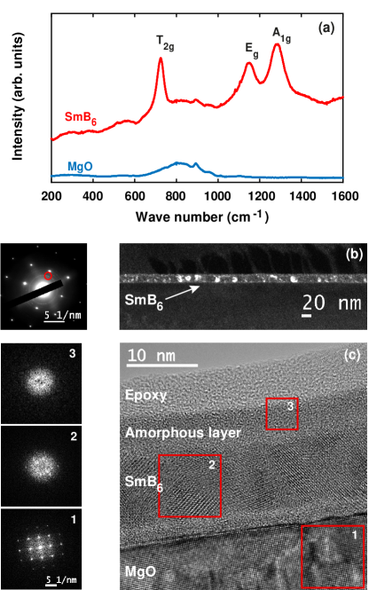
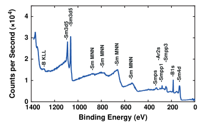
Thin film growth parameters were optimized using X-ray photoelectron spectroscopy measurements from which film stoichiometry was inferred and found to remain constant throughout the film thickness (see Appendix A). The film composition was also verified by energy dispersive X-ray spectroscopy and time-of-flight secondary ion mass spectrometry (ToF-SIMS) measurements, not shown here. Raman spectra measured with a 488 nm laser (Fig. 1 (a)) confirms the presence of first order Raman-allowed modes in SmB6 - T2g, Eg and A1g at 730, 1100 and 1200 cm-1 respectively Nyhus et al. (1997). To check the crystalline quality of our films, we have performed transmission electron microscopy (TEM) measurements, which revealed polycrystalline cubic structure of SmB6 with the Pm-3m (221) symmetry (see Fig. 1(b)-(c)). The dark field TEM image shows that crystallographic domain size ranges from several nanometers to around 10 nm, which is smaller than the film thickness. A layer of reduced crystallinity at the interface between the MgO substrate and SmB6 film is observed. The surface region of the film is of an amorphous structure due to oxidation as measured by energy-filtered TEM, possibly created during sample preparation for TEM measurements. Energy-filtered TEM measurements also confirm the correct stoichiometry and homogeneity of the film within error.
For transport measurements thin films with thickness ranging from 12 nm to 32 nm were used. For most samples, a precision diamond scriber was used to scribe 0.5 mm wide stripes to define current flow geometry that allowed simultaneous measurement of resistivity and Hall signals. For the 16 nm sample we also used photolithography with ion-milling to define a 100 m 260 Hall bar. Patterned and scribed samples gave qualitatively the same results. The magnetic field and current geometries are depicted in the inset of Fig. 2(c). Standard definitions for and are used. We took extra care to isolate the in-plane field effects from spurious effects caused by possible substrate misalignment or stage wobble. We always measured two devices simultaneously with a well defined angle between them (45∘ or 90∘). All effects reported here have the correct phase shift for the two corresponding bridges. We also measured in both positive and negative magnetic fields and symmetrized the data to eliminate spurious Hall contributions.
III Results and Discussion
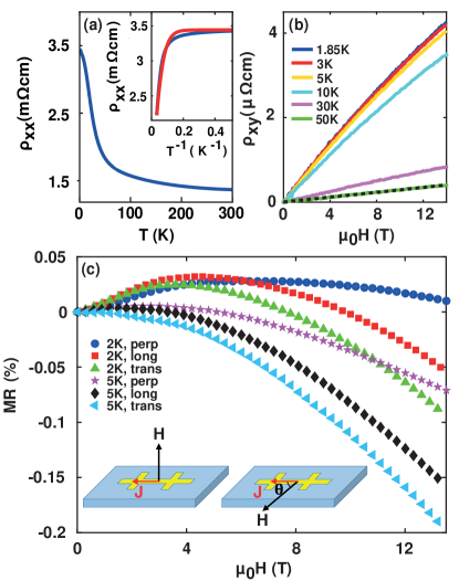
In Fig. 2(a) we present typical longitudinal resistivity () versus temperature data measured in the 16 nm thick Hall bar sample. The observed behavior is similar to previous reports and has been related to a Kondo insulating bulk with conducting surfaces.Syers et al. (2015); Wolgast et al. (2013) Taking into account the small sample thickness we find the resistance ratio (R(2 K)/R(300 K)) to be consistent with previous reports.Syers et al. (2015); Wolgast et al. (2013); Yong et al. (2014) In the inset we fit a simplified parallel conduction model,Wolgast et al. (2013); Syers et al. (2015) where the total sample resistivity consists of independent surface and bulk contributions: . Here, is the surface sheet resistance, is the bulk resistivity, kB is Boltzmann constant and is the excitation gap. We assume that is temperature independent and obtain meV from the fit shown in the inset of Fig. 2(a). This value does not change much with sample thickness and is consistent with other reports.Wolgast et al. (2013); Syers et al. (2015) Further analysis of sample resistance ratio as a function of thickness is consistent with coupling between opposite surfaces for thin films (see Appendix B).
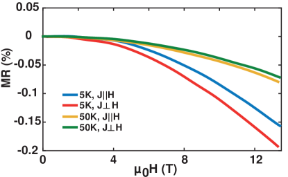
The Hall resistivity for various temperatures, is shown in Fig. 2(b). At high temperatures (), is linear with magnetic field indicating a single bulk channel conduction. For , the conduction is through both surface and bulk channels, which leads to non-linear . This multichannel conduction becomes weakest at the lowest measured temperature of 1.85 K, consistent with a dominant surface Hall conduction.Kim et al. (2013a) The magnetoresistance (MR) at 2 K and 5 K for various orientations is shown in Fig. 2(c). The overall behavior is consistent with Ref. Kim et al., 2014. The negative MR at high fields has been attributed to the reduction of the excitation gap by magnetic field and the liberation of bulk charge carriers.Cooley et al. (1995b) More data on the temperature dependence of the MR can be found in Appendix C.
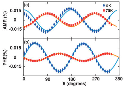
Figure 3 shows in-plane anisotropic magnetoresistance (AMR) and planar Hall effect (PHE) measurements at T = 5 K and T = 70 K for the 16 nm thick Hall bar sample. The measurement configuration is depicted in the right inset of Fig. 2(c), where the magnetic field lies in the sample plane. We have defined the AMR signal as: , where is the longitudinal resistivity in the presence of an in-plane magnetic field making an angle with the current density J. The averaged longitudinal resistivity over full field rotation, , comes out to be , where is the longitudinal resistivity for and is the transverse resistivity for . The PHE signal defined as , is merely a manifestation of AMR in the transverse voltage. Usually, this signal should be shifted by compared to the AMR signal as observed in Fig. 3. For a polycrystalline film, the AMR and PHE signals follow the expressions of the form:Thompson et al. (1975)
| (1) |
where is the normalized amplitude. The measured AMR and PHE signals fit quite well to Eq. 1, as shown in Fig. 3.
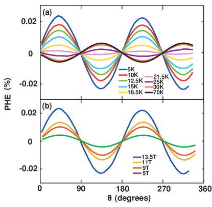
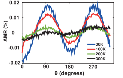
Surprisingly, the AMR signal has opposite signs for 5 K and 70 K. Namely, (positive AMR) at 5 K while at 70 K, (negative AMR). This sign change is observed in the PHE signal as well. We therefore carefully investigate the temperature dependence of this effect as shown in Fig. 4(a) for the 16 nm thick Hall bar sample. Between 70 K and 30 K, a negative signal with a negligible temperature dependence is observed. Around 23 K the AMR changes sign and as the temperature is lowered below 21.5 K, the AMR amplitude increases until it reaches a saturation value below (see Appendix D). The AMR amplitude decreases with decreasing field strength (see Fig. 4(b)), which can also be observed in Fig. 2(c).
We interpret our data as a result of a competition between surface and bulk AMR. As the temperature is lowered from 300 K to 70 K only the bulk exists, resulting in negative AMR. For 300 K T 70 K the AMR slowly increases with decreasing temperature, reaching roughly a constant value for temperatures between 70 K T 30 K (see Appendix D). At low temperatures the surface dominates over the bulk contribution and a positive AMR is seen.
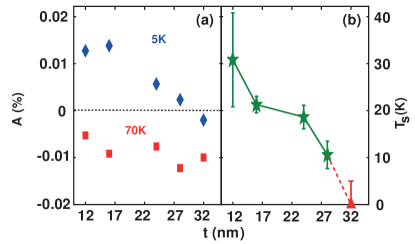
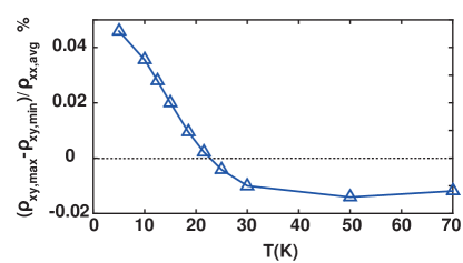
Since we are using thin films we can study the AMR as a function of film thickness. The thickness dependence of the AMR is shown in Fig. 5(a), where we plot the normalized amplitude (extracted from fitting of the PHE signal) at 5 K and at 70 K versus thickness, t. The normalized amplitude is roughly thickness independent at 70 K as expected for bulk effect. By contrast, the PHE amplitude decreases with increasing thickness at 5 K. We define Ts as the temperature at which the PHE changes sign. We plot Ts as a function of film thickness in Fig. 5(b) (see also Appendix E). Clearly, Ts decreases with increasing film thickness. For our 32 nm sample we did not find a sign change down to the lowest temperature measured.
The thickness dependence of the (positive) surface AMR suggests that it is related to coupling between opposite surfaces hosting states with opposite helicity. This coupling decreases with increasing thickness. The Fermi circles of these surface states can be slightly shifted due to the magnetic field Sulaev et al. (2015) or they can be different in size, e.g. due to different proximity to the substrate. We conjecture that magnetic field dependent scattering between such surfaces gives rise to the observed AMR. One can picture a mechanism somewhat similar to a two dimensional magnetic material with a Rashba-split bands as described in Ref. Trushin et al., 2009. While in Ref. Trushin et al., 2009 the two split bands are separated only in momentum space, in our case they are also spatially separated by the bulk of the film.
What is the mechanism for this inter-surface coupling? One possibility is tunneling.Pershoguba and Yakovenko (2012) Another coupling mechanism is phase coherent transport through the bulk enhanced by weak anti-localization (WAL).Not ; Lin et al. (2013) A third possibility is conduction via side surfaces, but this effect should be negligible for thin films. The relevant length-scale for tunneling is the wavefunction decay length, . It has been predicted that the surface states in SmB6 will remain topologically protected with decreasing thickness down to t 10 nm, due to surface Kondo breakdown.Alexandrov et al. (2015) For phase coherent transport enhanced by WAL one should consider the phase coherence length, Lϕ. These length scales should be compared to our film thickness.Kim et al. (2013b); Li et al. (2015) Recent reports estimated the dephasing length from WAL measurements in transverse magnetic fields to be of the order of 1 at 20 mK, which is much greater than our film thickness.Nakajima et al. (2016); Thomas et al. (2013) is expected to decrease as the temperature is increased by two orders of magnitude. At 300 mK is reported to be of the order of few tens of nanometers;Nakajima et al. (2016) not very far from our largest film thickness.
Both coupling mechanisms described above are consistent with the observed slow rise of surface-to-bulk sheet-resistance-ratio with decreasing thickness (see Appendix B). However, for the inter-surface coupling driven AMR to work, one would require the spin to be conserved while traveling through the bulk. We can therefore estimate the spin lifetime in the bulk of our films to be of the order of 5 10-14 seconds by dividing the thickness of the sample where the effect can be still observed by an average Fermi velocity taken from Ref. Li et al., 2014. Our result is longer than a naive estimation obtained from = /ESO, where is Planck constant and ESO is the spin-orbit energy in SmB6 ( 10-15 sec).Dzero et al. (2016)
The absence of positive AMR for the 32 nm thick film suggests that the surfaces are decoupled down to 5 K. We explain the small negative AMR observed at this temperature as a residual bulk AMR component. This bulk contribution is an order of magnitude smaller than the surface AMR and for thinner samples it is overwhelmed by the surface contribution. Finally, we note that T K determined from the AMR in our thinnest films is consistent with the temperature at which the surfaces states should be formed and with the amplitude of the excitation gap, .Kim et al. (2014)
The TEM measurement shows that the sample used for this study has an amorphous oxidized surface. This can result from the relatively long time elapsed from sample deposition to TEM measurement. The SmB6/MgO interface is far from being perfect and the sample is also found to be polycrystalline with many grain boundaries. Therefore, our three channel conduction description (two surfaces with coupling and bulk) is probably an oversimplification. But this model captures the main features and it is consistent with the resistivity versus temperature and Hall data.
IV Conclusion
We found that the in-plane anisotropic magnetoresistance (AMR) in thin films of SmB6 changes sign with temperature. We relate the negative AMR observed at high temperatures to a bulk signal, while the low temperature positive AMR is due to the surface states. The thickness dependence of the AMR and the temperature, Ts at which the AMR changes sign can be explained by gradual weakening of the coupling between non-trivial surfaces with increasing thickness. Our data therefore provide evidence for the existence of nontrivial surface states in SmB6 with a spin texture, which is distinct from the bulk. Finally, we estimate the spin life-time in the bulk to be of the order of seconds, an order of magnitude longer than the estimated spin-orbit scattering time.
Acknowledgements.
We thank A. Gladkikh for the TOF-SIMS measurements, Larisa Burstein for the XPS measurements and E. Greenberg for the Raman measurements. We are indebted to M. Goldstein for helpful discussions. This work was supported in part by the Israeli Science Foundation under grant no.569/13, by the Ministry of Science and Technology under contract 3-11875 and by the Pazy foundation.Appendix A X-ray Photoemission Spectroscopy measurements
The film growth parameters were optimized by using X-ray photoelectron spectroscopy (XPS) measurements from which the film stoichiometry was inferred. The sample was analyzed after sputter-cleaning for 1, 3 and 5 minutes using Ar+ ion gun. In Fig. 6 we show an XPS measurement of a 16 nm sample from which we extracted the correct stoichiometric ratio of 1:6 (Sm:B). The composition was found to remain constant as a function of sputtering time, indicating a uniform composition as a function of thickness.
Appendix B Inter-surface coupling
In order to study the surface contribution as a function of sample thickness, we plot the ratio as a function of in Fig. 7. This method gets rid of any uncertainty arising from the sample geometry. The ratio represents the relative surface-to-bulk ratio of the resistance, which is expected to be constant in an ideal case. However, the slow rise of this ratio with decreasing thickness indicates the gradual destruction of surface states, which can happen due to the coupling between opposite surfaces for thin films.
Appendix C Additional Magnetoresistance Measurements
Figure 8 shows the longitudional and transverse magnetoresistance for the 16 nm Hall bar sample (discussed in the main text), which further confirms the sign change of the AMR. Comparing the magnetoresistance data at low (5 K) and high temperature (50 K), the longitudinal magnetoresistance is greater than the transverse one at the low temperature regime , while at the high temperature regime they are reversed.
Appendix D Additional anisotropic magnetoresistance and planar hall effect Measurements
The temperature dependent PHE signals for 16 nm and 32 nm scribed samples are presented in Figs. 9(a) and 9(b) respectively. The 16 nm scribed sample exhibits similar temperature dependence as presented in Figs. 3 and 4 for the 16 nm Hall bar sample. Moreover, the AMR curves for 2 and 5 K are almost identical indicating low temperature saturation of surface AMR effect. In contrast, for the 32 nm sample the AMR always remains negative and no sign change is observed with decreasing temperature.
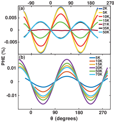
Fig. 10 presents the AMR measured in a 16 nm scribed sample for high temperatures. Upon increasing the temperature above 30 K, a slow decrease in the amplitude of the bulk negative AMR can be seen until the signal disappears between 200 K and 300 K.
Appendix E AMR transition temperature
To determine the temperature (Ts) at which the AMR changes sign, we have used the following method (See Fig. 11). We plot the measured amplitude of the PHE as a function of the temperature and interpolate to find where the measurement curve crosses zero amplitude. The error is set as half the separation between two measurement temperatures with opposite AMR signs closest to zero amplitude.
References
- Hasan and Kane (2010) M. Z. Hasan and C. L. Kane, Rev. Mod. Phys. 82, 3045 (2010).
- Qi and Zhang (2011) X.-L. Qi and S.-C. Zhang, Rev. Mod. Phys. 83, 1057 (2011).
- Dzero et al. (2010) M. Dzero, K. Sun, V. Galitski, and P. Coleman, Phys. Rev. Lett. 104, 106408 (2010).
- Takimoto (2011) T. Takimoto, Journal of the Physical Society of Japan 80, 123710 (2011).
- Menth et al. (1969) A. Menth, E. Buehler, and T. H. Geballe, Phys. Rev. Lett. 22, 295 (1969).
- Allen et al. (1979) J. W. Allen, B. Batlogg, and P. Wachter, Phys. Rev. B 20, 4807 (1979).
- Cooley et al. (1995a) J. C. Cooley, M. C. Aronson, Z. Fisk, and P. C. Canfield, Phys. Rev. Lett. 74, 1629 (1995a).
- Dzero et al. (2016) M. Dzero, J. Xia, V. Galitski, and P. Coleman, Annual Review of Condensed Matter Physics 7, 249 (2016).
- Kim et al. (2012) D. J. Kim, T. Grant, and Z. Fisk, Phys. Rev. Lett. 109, 096601 (2012).
- Wolgast et al. (2013) S. Wolgast, Ç. Kurdak, K. Sun, J. W. Allen, D.-J. Kim, and Z. Fisk, Phys. Rev. B 88, 180405 (2013).
- Kim et al. (2013a) D. J. Kim, S. Thomas, T. Grant, J. Botimer, Z. Fisk, and J. Xia, Scientific Reports 3, 3150 (2013a).
- Kim et al. (2014) D. J. Kim, J. Xia, and Z. Fisk, Nature Materials 13, 466 (2014).
- Syers et al. (2015) P. Syers, D. Kim, M. S. Fuhrer, and J. Paglione, Phys. Rev. Lett. 114, 096601 (2015).
- Neupane et al. (2013) M. Neupane, N. Alidoust, S.-Y. Xu, T. Kondo, Y. Ishida, D. J. Kim, C. Liu, I. Belopolski, Y. J. Jo, T.-R. Chang, et al., Nature Communications 4, 2991 (2013).
- Xu et al. (2013) N. Xu, X. Shi, P. K. Biswas, C. E. Matt, R. S. Dhaka, Y. Huang, N. C. Plumb, M. Radović, J. H. Dil, E. Pomjakushina, et al., Phys. Rev. B 88, 121102 (2013).
- Jiang et al. (2013) J. Jiang, S. Li, T. Zhang, Z. Sun, F. Chen, Z. Ye, M. Xu, Q. Ge, S. Tan, X. Niu, et al., Nature Communications 4, 3010 (2013).
- Frantzeskakis et al. (2013) E. Frantzeskakis, N. de Jong, B. Zwartsenberg, Y. K. Huang, Y. Pan, X. Zhang, J. X. Zhang, F. X. Zhang, L. H. Bao, O. Tegus, et al., Phys. Rev. X 3, 041024 (2013).
- Zhu et al. (2013) Z.-H. Zhu, A. Nicolaou, G. Levy, N. P. Butch, P. Syers, X. F. Wang, J. Paglione, G. A. Sawatzky, I. S. Elfimov, and A. Damascelli, Phys. Rev. Lett. 111, 216402 (2013).
- Zhang et al. (2013) X. Zhang, N. P. Butch, P. Syers, S. Ziemak, R. L. Greene, and J. Paglione, Phys. Rev. X 3, 011011 (2013).
- Yee et al. (2013) M. M. Yee, Y. He, A. Soumyanarayanan, D.-J. Kim, Z. Fisk, and J. E. Hoffman (2013), eprint arXiv:1308.1085v2.
- Ruan et al. (2014) W. Ruan, C. Ye, M. Guo, F. Chen, X. Chen, G.-M. Zhang, and Y. Wang, Phys. Rev. Lett. 112, 136401 (2014).
- Thomas et al. (2013) S. Thomas, D. J. Kim, S. B. Chung, T. Grant, and J. Fisk, Z. Xia (2013), eprint arXiv:1307.4133.
- Nakajima et al. (2016) Y. Nakajima, P. Syers, X. Wang, R. Wang, and J. Paglione, Nature Physics 12, 213 (2016).
- Li et al. (2014) G. Li, Z. Xiang, F. Yu, T. Asaba, B. Lawson, P. Cai, C. Tinsman, A. Berkley, S. Wolgast, Y. S. Eo, et al., Science 346, 1208 (2014).
- Tan et al. (2015) B. S. Tan, Y.-T. Hsu, B. Zeng, M. C. Hatnean, N. Harrison, Z. Zhu, M. Hartstein, M. Kiourlappou, A. Srivastava, M. D. Johannes, et al., Science 349, 287 (2015).
- Yong et al. (2014) J. Yong, Y. Jiang, D. Usanmaz, S. Curtarolo, X. Zhang, L. Li, X. Pan, J. Shin, I. Takeuchi, and R. L. Greene, Applied Physics Letters 105, 222403 (2014).
- Nyhus et al. (1997) P. Nyhus, S. L. Cooper, Z. Fisk, and J. Sarrao, Phys. Rev. B 55, 12488 (1997).
- Cooley et al. (1995b) J. C. Cooley, M. C. Aronson, A. Lacerda, Z. Fisk, P. C. Canfield, and R. P. Guertin, Phys. Rev. B 52, 7322 (1995b).
- Thompson et al. (1975) D. Thompson, L. Romankiw, and A. Mayadas, IEEE Transactions on Magnetics 11, 1039 (1975), ISSN 0018-9464.
- Sulaev et al. (2015) A. Sulaev, M. Zeng, S.-Q. Shen, S. K. Cho, W. G. Zhu, Y. P. Feng, S. V. Eremeev, Y. Kawazoe, L. Shen, and L. Wang, Nano Letters 15, 2061 (2015).
- Trushin et al. (2009) M. Trushin, K. Výborný, P. Moraczewski, A. A. Kovalev, J. Schliemann, and T. Jungwirth, Phys. Rev. B 80, 134405 (2009).
- Pershoguba and Yakovenko (2012) S. S. Pershoguba and V. M. Yakovenko, Phys. Rev. B 86, 165404 (2012).
- (33) WAL in the presence of in-plane magnetic field is caused by finite penetration depth of the surface states into the bulk, due to the small excitation gap of SmB6 Nakajima et al. (2016).
- Lin et al. (2013) C. J. Lin, X. Y. He, J. Liao, X. X. Wang, V. S. IV, W. M. Yang, T. Guan, Q. M. Zhang, L. Gu, G. Y. Zhang, et al., Phys. Rev. B 88, 041307 (2013).
- Alexandrov et al. (2015) V. Alexandrov, P. Coleman, and O. Erten, Phys. Rev. Lett. 114, 177202 (2015).
- Kim et al. (2013b) D. Kim, P. Syers, N. P. Butch, J. Paglione, and M. S. Fuhrer, Nature Communications 4, 2040 (2013b).
- Li et al. (2015) Z. Li, I. Garate, J. Pan, X. Wan, T. Chen, W. Ning, X. Zhang, F. Song, Y. Meng, X. Hong, et al., Phys. Rev. B 91, 041401 (2015).