Influence of twist boundary on deformation behaviour of 100 BCC Fe nanowires
Molecular dynamics simulations revealed significant difference in deformation behaviour of 100
BCC Fe nanowires with and without twist boundary. The plastic deformation in perfect 100 BCC Fe
nanowire was dominated by twinning and reorientation to 110 followed by further deformation by
slip mode. On the contrary, 100 BCC Fe nanowire with a twist boundary deformed by slip at low
plastic strains followed by twinning at high strains and absence of full reorientation. The results
suggest that the deformation in 100 BCC Fe nanowire by dislocation slip is preferred over twinning
in the presence of initial dislocations or dislocation networks. The results also explain the absence
of extensive twinning in bulk materials, which inherently contains large number of dislocations.
Keywords: Molecular dynamics simulations; BCC Fe nanowire; Twist boundary; Twinning and slip
1 Introduction
In recent years, metallic nanowires have attracted a major attention for research due to their unique properties and potential applications in future nano/micro electro-mechanical systems (NEMS/MEMS). Due to good magnetic properties, BCC Fe nanowires in particular find applications in high-density magnetic recording media, data storage and memory devices, spin electronics and smart sensors [3, 4]. The reorientation and the associated pseudo elastic and shape memory behaviour of nanowires originating from deformation by twinning facilitate important applications in smart sensors. In view of this, it is essential to understand the occurrence of twinning and the factors that influences the twinning mode of deformation in metallic nanowires.
Deformation twinning usually occurs under conditions that lead to high stresses such as high strain rates or low temperatures [5]. Twinning in perfect nanowires occurs due to high stresses resulting from small size and the exhaustion of dislocation sources [6, 7]. Several experimental [8, 9] and atomistic simulation studies [10, 11, 12, 13] have shown that both FCC and BCC metallic nanowires deform by twinning mechanism. Using in-situ scanning electron microscopy and high-resolution transmission electron microscopy, it has been shown that the plastic deformation in defect-free Au nanowire with 110 orientation occurs by twinning mechanism [8]. In agreement with experimental studies, the atomistic simulations also revealed deformation dominated by twinning in Cu, Au and Ni nanowires with 110 orientation under tensile loading [10, 11, 14]. It has also been shown that twinning occurs in 100 Cu, Au and Ni nanowires under compressive loading [10]. Similar to FCC nanowires, Wang et al. [9] reported the first experimental evidence of deformation twinning in BCC nanowires. It has been shown that the deformation occurs by twinning under tensile loading in 100 orientation and under compressive loading in 110 and 111 orientations in BCC W nanowires [9]. Molecular dynamics simulations have also shown that the deformation proceeds by twinning under tensile loading in 100 BCC Fe, Mo and W nanowires [12, 13, 15, 16, 17]. In both FCC and BCC nanowires, deformation by twinning leads to reorientation, pseudo-elasticity, shape memory and super-elasticity [12, 14, 15, 18, 19, 20]. Most of these studies were focused on perfect nanowires, and it is not clear whether the deformation by twinning will continue to occur in the presence of defects such as dislocations and grain boundaries. Recently, it has been shown that the presence of twin boundary in 110 FCC Cu nanopillars changes the deformation mechanism from twinning to slip [21]. In the present study, an attempt has been made to understand the influence of twist boundary on deformation twinning in BCC Fe nanowires.
2 MD simulation details
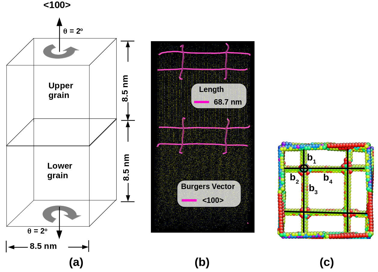
Molecular dynamics simulations have been carried out using large-scale atomic/molecular massively parallel simulator (LAMMPS) package [22], and the visualization of atomic structure was accomplished using AtomEye [23] package. The Burgers vector and the total length of dislocations have been determined using OVITO [24]. Initially, single crystal BCC Fe nanowires oriented in 100 axial direction with {100} side surfaces were created. The nanowire had dimensions of nm3 consisting of about 110,000 atoms arranged in a BCC lattice and interacting through an embedded atom method (EAM) potential developed by Mendelev et al. [25]. Following the creation of perfect nanowire, the nanowire is divided into two equal upper and lower grains along the nanowire axis (Figure 1a). In order to introduce a twist boundary, the upper grain is rotated by an angle and lower grain by around the nanowire axis. Upon relaxation, a screw dislocation network was spontaneously formed at the interface separating upper and lower grains (Figure 1b and c). The second network at the top appears due to the periodic boundary conditions. The choice of twist angle of was based on earlier study [26] on the formation of initial dislocation network structure in BCC Fe. The dislocation network has square structure (four-fold symmetry) with junctions formed by four 100 type sessile screw dislocations and shown in Figure 1c. The Burger vectors of dislocations at the junction satisfy the relation . Following the creation of {100} twist boundary, initial velocities were assigned randomly to all the atoms according to finite temperature Maxwell distribution and then the system was equilibrated to 10 K in canonical ensemble (constant NVT). The velocity verlet algorithm was used to integrate the equation of motion with a time step of 2 fs. Upon completion of equilibration process, tensile deformation was carried out at a constant engineering strain rate of s-1 along the nanowire axis. The average stress is calculated from the Virial expression [27].
3 Results and discussion
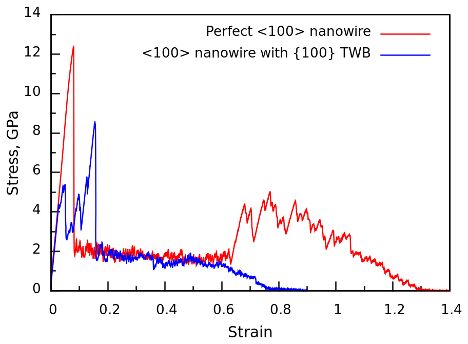
The stress-strain behaviour of 100 BCC Fe nanowire with {100} twist boundary along with perfect nanowire under tensile loading is shown in Figure 2. Both the nanowires displayed similar elastic deformation at low strains having elastic modulus of 164 GPa. The Young’s modulus value of 164 GPa for perfect 100 BCC Fe nanowire is in good agreement with those obtained using MD simulations [13] and Ab-initio calculations [28]. The perfect nanowire exhibited large elastic deformation and higher yield strength compared to that displayed by nanowire with a twist boundary. The yield strength of 12.4 GPa obtained for perfect nanowire is close to the theoretical strength of BCC Fe in 100 direction [29] and the yielding leads to an abrupt large drop in flow stress to about 2 GPa. BCC Fe nanowire with {100} twist boundary displayed comparatively small elastic deformation along with lower yield strength of 5.3 GPa and lower strain to yielding () compared to perfect nanowire. Following the initial yielding, the two nanowires exhibited contrasting flow behaviour during plastic deformation. A constant flow stress of 2 GPa up to followed by a second elastic peak, yield drop and continuous decreases in flow stress till failure was observed in the perfect BCC Fe nanowire. Contrary to this, the nanowire containing a twist boundary exhibited large flow stress fluctuations at low strains followed by a second elastic peak with peak stress value 8.6 GPa and yield drop at . After second yield drop, a constant but marginally lower flow stress of 1.8 GPa up to followed by decrease in flow stress till failure was observed. It can be seen in Figure 2 that nanowire with twist boundary has a significantly lower strain to failure than perfect nanowire.
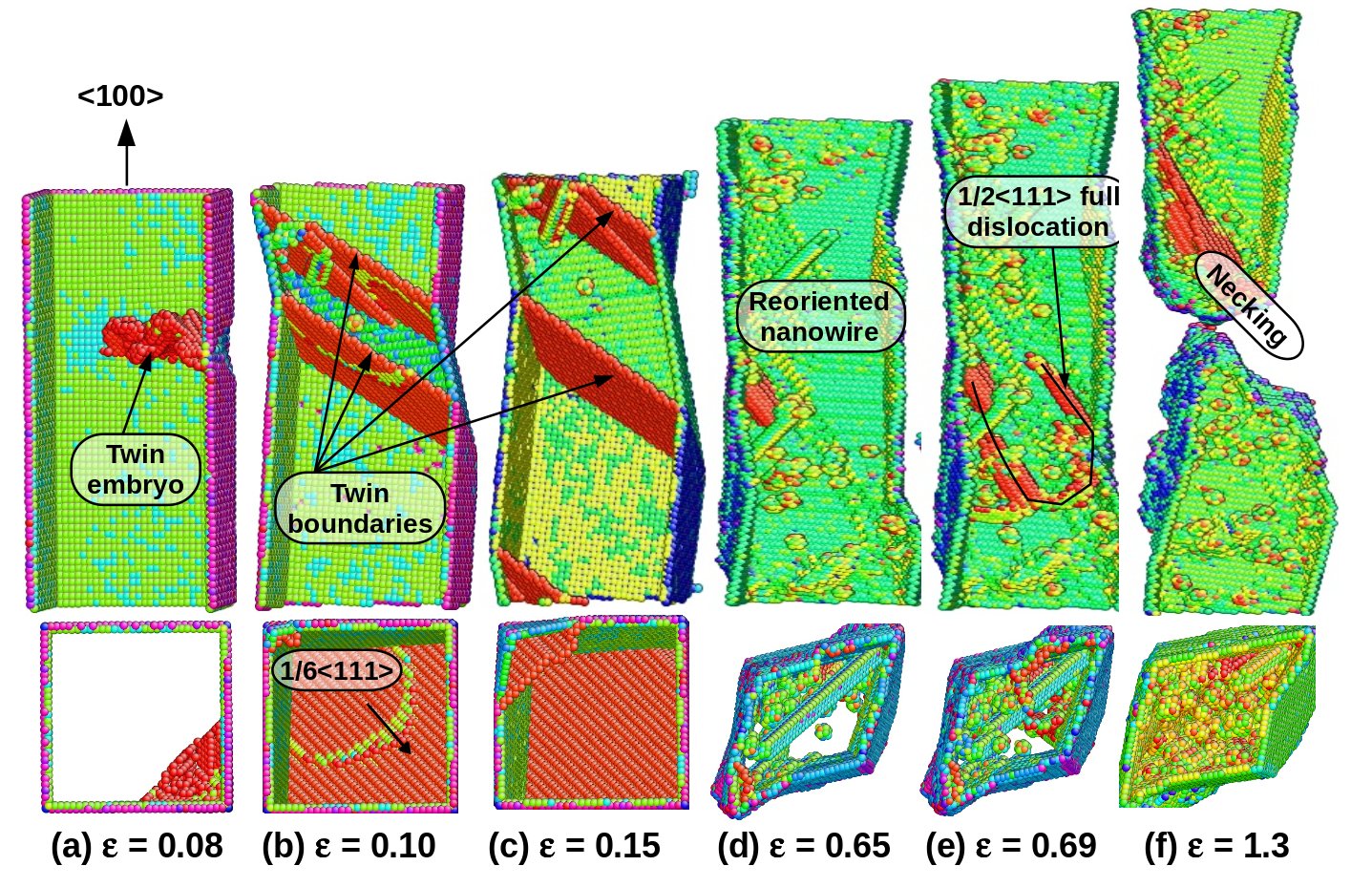
The atomic snapshots displaying the deformation behaviour of perfect BCC Fe nanowires at 10 K are shown in Figure 3. The nanowire yielded by the nucleation of a twin embryo from the corner on {112} plane with a twin front propagating in 111 direction is seen in Figure 3a. Once the twin front reaches the opposite surface, the twin embryo becomes a full twin enclosed by two twin boundaries (Figure 3b). Along these twin boundaries, the 1/6111 twinning partial dislocations move in opposite directions and displace the twin boundaries away from each other. As a result, the twin grows plane by plane along the nanowire axis (Figure 3c). Since twin growth process does not create any new surface, the flow stress plateau during the twin growth is observed (Figure 2). In the absence of obstacles, the twin boundaries easily sweep across the nanowire and due to periodic boundary conditions along the length, they meet each other and annihilate. This leads to reorientation of initial 100 nanowire to 110 nanowire (Figure 3d) along with a change in cross-section shape from square (Figure 3a-c) to rhombic (Figure 3d-f). Following reorientation, 110 nanowire undergoes an elastic deformation at with lower modulus (Figure 2) and yielding by the nucleation of 1/2111 full dislocations is shown in Figure 3e. Further plastic deformation in the reoriented nanowire occurs by dislocation slip mechanism till failure (Figure 3e-f). Following second yielding, the necking initiates at the strain value of 0.95 followed by continuous decrease in flow stress (Figure 2) associated with the growth of necking leading to failure (Figure 3f).
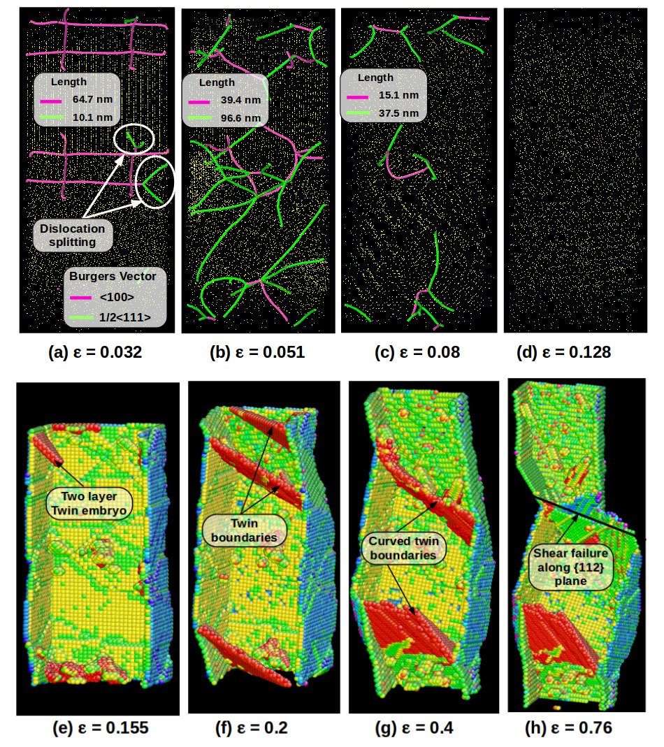
The deformation behaviour of BCC Fe nanowire with twist boundary at 10 K is shown in Figure 4. During elastic deformation, no change in the initial dislocation network structure has been observed. The yielding occurs by splitting 100 type sessile screw dislocations into two 1/2111 glissile dislocations (Figure 4a). As a result, the decrease in total length of 100 dislocations from 68.7 to 64.7 nm at an expense of 1/2111 dislocations is seen (Figure 4a). The splitting of sessile screw dislocations initiates from the surface of the nanowire and penetrates towards the dislocation junction. With increasing plastic strain, more and more sessile dislocations splits into glissile dislocations and move away from the initial network (Figure 4b). This continuous splitting increases the total length of 1/2111 glissile dislocations from 10.1 nm at yielding () to 96.6 nm at with corresponding decrease in 100 sessile dislocations. Energetically, the splitting of 100 dislocations is difficult to be observed at low stresses due to increase in energy, i.e. . However, this dislocation reaction becomes feasible at high stresses typically in the order of GPa as observed in the present study. The continuous splitting of 100 network dislocations followed by glide of resultant dislocations and their escape to surface leads to small elastic peaks and flow stress drops at low strains in the range 0.032-0.15 (Figure 2). The presence of high surface and image stresses aided by small size facilitates dislocations to escape from the nanowire. As a result, the total length of 1/2 111 glissile dislocations also decreases from a peak of 96.6 nm at (Figure 4b) to 37.5 nm at (Figure 4c). The continuous split and escape of dislocations leave the nanowire in a dislocation-free state (Figure 4d) with a few point defects. At this stage, an increase in plastic strain leads to second elastic deformation with peak stress value of 8.6 GPa followed by an abrupt drop in the flow stress. This abrupt drop due to the yielding of dislocation-free nanowire takes place by the nucleation of two-layer twin embryo from the slip step as shown in Figure 4e. With increasing plastic deformation, the two layer twin embryo becomes a full twin enclosed by two twin boundaries as shown in Figure 4f. This twin boundaries move away from each other (Figure 4g) by the repeated initiation and glide of 1/6111 twinning partial dislocations resulting in the constant flow stress with some oscillations in the strain range 0.15-0.6 (Figure 2). Due to the presence of point defects generated by the movement of 1/2111 dislocations during initial deformation by slip mode, the twin boundary migration or twin growth process is impeded and as a result, the nanowire does not undergo full reorientation and fails by shearing along the {112} twin boundary plane (Figure 4h). The strain for the onset of necking has been obtained as 0.62. These results indicate that the nanowire containing a twist boundary deforms by slip at small strains followed by twinning at large strains. The simulations performed on nanowire with multiple twist boundaries with smaller twist boundary spacing also indicated similar deformation behaviour. Further, MD simulations performed at higher temperatures of 300 and 600 K indicated that the perfect nanowire and the nanowire containing a twist boundary undergo deformation similar to that at 10 K.
The perfect 100 BCC Fe nanowire and the nanowire containing a twist grain boundary display significant difference in stress-strain behaviour as well as in operating deformation mechanism. The perfect nanowire displays two elastic peaks separated by twinning mode of deformation over large plastic strain. In nanowire containing twist boundary, the elastic peaks are separated by dislocation slip over small plastic strain. Further, the origin of the second peak is different in these two nanowires. In perfect nanowire, it is due to the elastic deformation of the reoriented nanowire, while in nanowire containing twist boundary, it is due to elastic deformation of dislocation-free nanowire. The deformation behaviour of perfect nanowire is in agreement with those reported in perfect 100 BCC Fe, Mo, and W nanowire [12, 13, 15, 16, 17, 30]. This difference in deformation behaviour arises mainly from the presence of initial dislocation network at twist boundary facilitating dislocation slip mechanism at small strains. The continuous splitting of 100 network sessile dislocations into glissile dislocations and their escape to surface leads to dislocation free nanowire close to the perfect one. Following this, twinning takes over as the dominant mode of deformation. These results indicate that the presence of initial dislocations has dominant effect on twinning mechanism. It has been observed that the deformation by slip of full dislocations is preferred over twinning in the presence of dislocations or dislocation networks. The study also substantiates the absence of deformation twinning generally observed in bulk materials, which inherently contain many dislocations.
4 Conclusion
Molecular dynamics simulation results indicate that the presence of {100} twist boundary in 100 BCC Fe nanowire influences the operating deformation twinning mechanism and the associated reorientation process. The perfect BCC Fe nanowire deformed by twinning mechanism leading to the reorientation of the nanowire, while nanowire containing twist grain boundary deformed by slip at low strains followed by twinning at high strains and absence of reorientation. At low strains, deformation by slip of full dislocations is preferred over twinning in nanowires containing initial dislocations or network dislocations. The splitting of 100 network sessile dislocations into glissile dislocations and their escape to surface leads to dislocation free nanowire, which further deform by twinning at high strains. The study also supports the absence of twinning in material containing initial dislocations, such as bulk single crystals and bi-crystals with twist boundaries.
References
- [1]
- [2]
- [3] J.I. Martin, J. Nogues, K. Liu, J.L. Vicent and I.K. Schuller, J. Magn. Magn. Mater. 256 (2003) p. 449.
- [4] X.Y. Zhang, G.H. Wen, Y.F. Chan, R.K. Zheng, X.X. Zhang and N. Wang, Appl. Phys. Lett. 83 (2003) p. 3341.
- [5] J.W. Christian and S. Mahajan, Prog. Mater. Sci. 39 (1995) p. 1.
- [6] Q. Yu, L. Qi, K. Chen, R.K. Mishra, J. Li and A.M. Minor. Nano Lett. 12 (2012) p. 887.
- [7] D. Kiener and A.M. Minor. Nano Lett. 11 (2011) p. 3816.
- [8] S.H. Seo et al. Nano Lett. 11 (2011) p. 3499.
- [9] J. Wang, Z. Zeng, C.R. Weinberger, Z. Zhang, T. Zhu and S.X. Mao, Nat. Mater. 14 (2015) p. 594.
- [10] H.S. Park, K. Gall and J.A. Zimmerman, J. Mech. Phys. Solids 54 (2006) p. 1862.
- [11] C.R. Weinberger and W. Cai, J. Mater. Chem. 22 (2012) p. 3277.
- [12] S. Li, X. Ding, J. Deng, T. Lookman, J. Li, X. Ren, J. Sun and A. Saxena, Phy. Rev. B 82 (2010) 205435.
- [13] G. Sainath and B.K. Choudhary, Comp. Mater. Sci. 111 (2016) p. 406.
- [14] W. Liang and M. Zhou, Phys. Rev. B 73 (2006) 115409.
- [15] A. Cao, J. Appl. Phys. 108 (2010) 113531.
- [16] P. Wang, W. Chou, A. Nie, Y. Huang, H. Yao and H. Wang, J. Appl. Phys. 110 (2011) 093521.
- [17] C.J. Healy and G.J. Ackland, Acta Mater. 70 (2014) p. 105.
- [18] H.S. Park, K. Gall and J.A. Zimmerman, Phys. Rev. Lett. 95 (2005) 255504.
- [19] V.K. Sutrakar, D.R. Mahapatra and A.C.R. Pillai, J. Phys. Condens. Matter. 24 (2012) 015401.
- [20] J. Zhu and D. Shi, J. Phys. D: Appl. Phys. 44 (2011) 055404.
- [21] G. Sainath and B.K. Choudhary, Phys. Lett. A 379 (2015) p. 1902.
- [22] S. Plimpton, J. Comp. Phy. 117 (1995) p. 1.
- [23] J. Li, Modell. Simul. Mater. Sci. Eng. 11 (2003) p. 173.
- [24] A. Stukowski, Modell. Simul. Mater. Sci. Eng. 18 (2010) p.015012.
- [25] M.I. Mendelev, S. Han, D.J. Srolovitz, G.J. Ackland, D.Y. Sun and M. Asta, Phil. Mag. 83 (2003) p. 3977.
- [26] J. Hetherly, E. Martinez, M. Nastasi and A. Caro, J. Nucl. Mater. 419 (2011) p. 201.
- [27] J.A. Zimmerman, E.B. Webb, J.J. Hoyt, R.E. Jones, P.A. Klein and D.J. Bammann, Modell. Simul. Mater. Sci. Eng. 12 (2003) p. S319.
- [28] M. Friak, M. Sob and V. Vitek, Phil. Mag. 83 (2003) p.3529.
- [29] D.M. Clatterbuck, D.C. Chrzan and J.W. Morris Jr., Acta Mater. 51 (2003) p. 2271.
- [30] G. Sainath, B.K. Choudhary and T. Jayakumar, Comp. Mater. Sci. 104 (2015) p. 76.