Controlling the growth of Bi(110) and Bi(111) films on an insulating substrate
Abstract
Here we demonstrate the controlled growth of Bi(110) and Bi(111) films on an (insulating) -Al2O3(0001) substrate by surface X-ray diffraction and X-ray reflectivity using synchrotron radiation. At temperatures as low as 40 K, unanticipated pseudo-cubic Bi(110) films are grown having a thickness ranging from a few to tens of nanometers. The roughness at the film-vacuum as well as at the film-substrate interface, can be reduced by mild heating, where a crystallographic orientation transition of Bi(110) towards Bi(111) is observed at 400 K. From 450 K onwards high quality and ultrasmooth Bi(111) films are formed. Growth around the transition temperature results in the growth of competing Bi(110) and Bi(111) thin film domains.
I Introduction
Nanostructured ultrathin Bi films have recently attracted a lot of interest as they reveal exotic magneto-electronic properties making them appealing materials for spintronic applications Hofmann (2006); Koroteev et al. (2008); Xiao et al. (2012); Yang et al. (2012); Ando (2013); Sabater et al. (2013); Aitani et al. (2014); Drozdov et al. (2014); Aguilera et al. (2015); Miao et al. (2015); Du et al. (2016); Reis et al. (2016). Especially the spin-momentum locked surface states of topological insulating Bi films Song et al. (2015); Lu et al. (2015); Yao et al. (2016); Bian et al. (2016), make them very attractive candidates for spintronic devices. To develop and optimize topological insulators (TIs) towards applications, thin films of high quality are a necessity, as otherwise the exotic electronic properties are hampered by bulk conduction Liu et al. (2011); Aitani et al. (2014); Lima and Schmidt (2015). To minimize the contribution of the substrate Miao et al. (2015), an atomically well defined insulating substrate, providing an infinite potential well barrier, is essential for both future electronic applications as well as to get a deeper understanding on the controllability of Bi growth. This choice of substrate is also very beneficial for practical applications, as the interface between film and insulating substrate, expected to reveal topological states, will also be protected from influencing oxidation effects arising from ambient exposure in technological applications Tabor et al. (2011). The growth of Bi has been extensively studied on Si(111) Tanaka et al. (1999); Nagao et al. (2000); Yaginuma et al. (2003); Nagao et al. (2004); Kammler and von Hoegen (2005); M nig et al. (2005); Nagao et al. (2005); Yaginuma et al. (2007); Lükermann et al. (2014); Kokubo et al. (2015) and HOPG Scott et al. (2005); McCarthy et al. (2010); Kowalczyk et al. (2011); Song et al. (2015) as well as other surfaces Jeffrey et al. (2006); Kim et al. (2006); Hattab et al. (2008); Payer et al. (2008); Zhang et al. (2009a); Bobaru et al. (2012); Xiao et al. (2012); Yang et al. (2012); Reis et al. (2016), resulting in fabrication of films with a range of different morphologies, orientations, and strain. The fabrication of Bi films has attracted considerable interest in recent years, as their controlled growth, with focus on morphology and crystallographic orientation, on semiconductor and oxide surfaces is not a trivial task. It is well-known that metals on semiconductors and oxides usually show 3D growth modes Campbell (1997) instead of atomically smooth (2D) films. However, this problem can be overcome by use of deposition at low temperatures Ernst et al. (1993); Campbell (1994) or surfactant-mediated growth Rosenfeld et al. (1993); Zhang (1997), as it modifies the film kinetics.
In this study we demonstrate by surface X-ray diffraction (SXRD) the controlled growth of thin Bi(110) and Bi(111) films (the index used throughout this paper refers to the rhombohedral system) on such an insulating substrate: atomically smooth insulating sapphire (-Al2O3(0001)) having a lattice mismatch of 4.6% with Bi(111), so large that thermal mismatch might be ignored. The preparation of pseudo-cubic (110)-oriented Bi films, a rather exotic orientation, is a difficult task Wu and Chern (2008). At temperatures as low as 40 K, we are able to slow down kinetics resulting in a high nucleation density of Bi islands and thereby controlling the growth of Bi towards smooth Bi(110) films, stable up to 400 K. By annealing the Bi(110) films beyond this temperature, they can be transformed towards stable Bi(111) films. For films grown around RT, a competition between (110) and (111) thin film domains is observed.
II Experimental
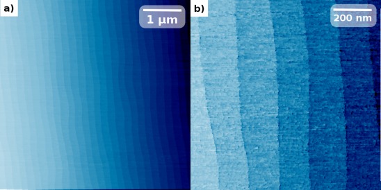
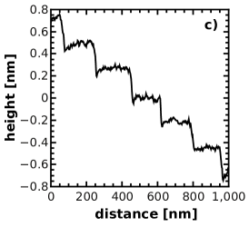
For the surface X-ray diffraction (SXRD) experiments described here, we used hat shaped -Al2O3(0001) single crystals with a miscut of 0.2∘. Prior to annealing for 12 hours in a tube furnace at 1323 K using an O2 flow of 150 l/h, the samples have been ultrasonically degreased in acetone and ethanol. The samples were then initially inspected by tapping mode atomic force microscopy (TM-AFM) for their stepheight (0.21 nm between two adjacent oxygen planes) and terrace width (300 nm,) and X-ray photoelectron spectroscopy (XPS) to verify the surface cleanliness where only minor traces of C and Ca were found, see Supplemental Material. After insertion into the UHV system of the surface diffraction beamline ID03/ESRF (Grenoble, France) Balmes et al. (2009) with a base pressure below 110-10 mbar, the sample was cleaned by mild 700 eV Ar+ sputtering at mbar and subsequent annealing to 1200 K in an O2 background pressure of mbar cycles, where we monitored the sample quality by Auger electron spectroscopy (AES), see Supplemental Material. Bi was deposited at a typical deposition rate of 1.3Å per minute from a Mo crucible mounted inside an electron-beam evaporator (Omicron EFM-3). According to the bulk phase diagram, Bi and sapphire are immiscible in the bulk Okamoto (1991). The surface X-ray diffraction (SXRD) experiments were performed using a monochromatic synchrotron X-ray beam at 24 keV and a MAXIPIX detectorPonchut et al. (2011) with 512512 pixels. For data integration and the creation of reciprocal space maps from the 2D detector frames we used the BINoculars software package Roobol et al. (2015). All reciprocal space positions are given in (h,k,l) measured in reciprocal lattice units (r.l.u.) of the hexagonal substrate (0001) surface lattice. Bragg peaks of the thin Bi films are labeled by their conventional rhombohedral Miller indices Hofmann (2006). X-ray reflectivity (XRR) curves have been fitted using the GenX software package Björck and Andersson (2007).
III Results
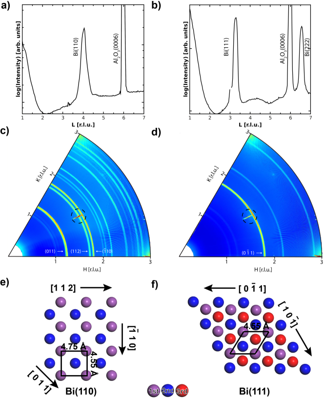
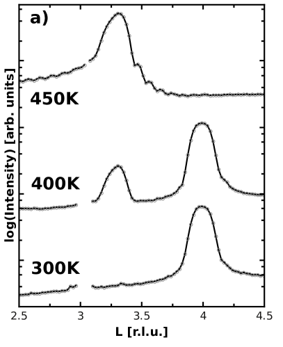
In order to determine the surface structure and morphology of the thin Bi films grown in-situ, we make use of XRR scans, crystal truncation rod (CTR) scans and reciprocal space maps determined by SXRD. The out-of-plane (electronic) density profile measured by XRR provides information on film layer density, film thickness and interface roughness. The measured (00) crystal truncation rod (CTR) provides information on the out-of-plane crystallographic orientation of the film. To be sensitive to the in-plane registry we record reciprocal spacemaps (at constant L=0.3). In Fig. 1(a-b) and (c-d) we show the (00) CTR and reciprocal space map of thin Bi films grown on the sapphire substrate. A sharp pronounced (0006) Bragg peak in (a-b) corresponds to the out-of-plane interlayer distance of the sapphire (0001) surface unit cell. Upon growth of a 20 nm thick film at 40 K, a Bragg-peak is found at L=4 corresponding to the 3.25Å interlayer distance of Bi(110) Hofmann (2006), see Fig. 1(a). In the reciprocal space map, see Fig. 1(c), rings appear caused by the rotational disorder of the Bi(110) domains. The position of the rings perfectly matches to the (011), (112) and (0) Bi planes expected for the Bi(110) surface, as depicted in Fig. 1(e), and corresponding to in-plane distances of 3.28Å, 4.75Å and 4.55Å.
Annealing the as grown film up to 400 K, results in the repositioning of the Bi Bragg peak in the recorded (00) CTR to L=3.3, corresponding to the interlayer distance of 3.94Å for Bi(111) Hofmann (2006), see Fig. 1(b). The corresponding reciprocal space map is shown in Fig. 1(d). For this film, also ring structures in the diffracted intensity appear, with the most intense ring position matching the (01) plane, see Fig. 1(f), and corresponding to an in-plane distance of 4.55Å. Analogue to the Bi(110) film, the presence of the rings results from rotational disordered Bi(111) domains on the surface. The Bi(111) domains show slight preferential alignment with respect to the six-fold symmetric substrate as can be seen from the increased intensity on the ring close to the (11) CTR, see Fig. 1(d).
| T(K) | Bi film structure | (Å) | (Å) | (Å) |
|---|---|---|---|---|
| 40 | (110) | 7.2 | 8.1 | 142 |
| 120 | (110) | 5.5 | 9.1 | 143 |
| 300 | (110) | 4.4 | 3.3 | 140 |
| 400 | (110) & (111) | 4.8 | 3.2 | 138 |
| 450 | (111) | 1 | 5.7 | 136 |
| 475 | (111) | 1 | 3.2 | 137 |
| 500 | (111) | 1 | 2.6 | 137 |
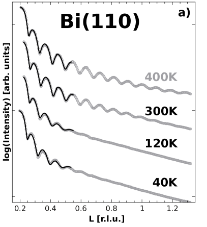
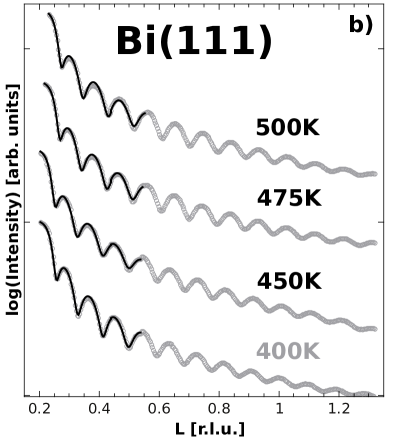
To test both the Bi(110) and Bi(111) film for their thermal stability and to investigate the effects of kinetics on the film roughness, we deposited 14 nm of Bi on the sapphire surface at 40 K and gradually increased the temperature. Fig. 2(a) shows XRR curves, revealing the effect of increasing the temperature. At higher temperature, the number of Kiessig fringes and their amplitude, arising from the constructive interference between the X-rays reflected from the film-vacuum and substrate-film interface, increases, indicating the decrease in roughness on both interfaces. At 400 K, the Kiessig fringes are also visible beyond L=1.3. The film consists at this temperature of Bi(110) and Bi(111) domains, discussed below. The reason for the Bi(110) films not transforming below 400 K are the slowed kinetics Campbell (1997). When heating the same film beyond 400 K, the film shows a pure Bi(111) crystal structure of which the number of Kiessig fringes increase even beyond the film Bragg peak at L=3.3, see also Fig. 3(a), for temperatures at 500 K and above (but below the film melting temperature of 545 K depending on film thickness Takagi (1954)).
In order to quantify the roughness for the film-vacuum and substrate-film interface, we model the system as a film of uniform (electronic) density on top of a uniform (electronic) dense substrate. Fitting was done by using the fitting parameters film thickness (), film-vacuum interface roughness (), substrate-film interface roughness () (see Tab. 1), a background resulting from scattering and a normalization factor Björck and Andersson (2007). Note that we fit up to limited L (here 0.6) to ensure the dynamical scattering theory is applicable and stay far from the kinetical scattering regime Vlieg (2012).
The roughness for the Bi(110) film-vacuum interface can be reduced by about 40% to 4.4Å by heating the sample to RT, see Tab. 1. The can also be greatly reduced, which may be indicative of the rough initial growth due to the lattice mismatch described above, resulting in an electronic gradient in the profile going from substrate to film. Upon heating, these lattice defects might be restored and the film might be (more) decoupled from its substrate as the roughness for the Bi(110) film at RT is similar to Bi(111) films. The ultrasmooth Bi(111) films, having a below 1Å, also reveal a decreasing upon increasing temperature. Note, that the used modeling only includes a fixed and homogenous electronic density value for vacuum, film and substrate, giving a very reasonable fit as shown by the solid curves in Fig. 2(a) and (b). This means that the electronic density profile is close to a step function, indicating the decoupling of electronic density between substrate and film.
A striking feature in the growth of Bi on sapphire is the appearance of the Kiessig fringes when the film is deposited at 40 K, in contrast to films deposited at RT and above. We expect this to result from 2D island growth as described by Campbell for the growth of metals on oxide surfaces Campbell (1997). According to this model, due to the low temperature, the kinetic limitations cause a high nucleation density resulting initially in 2D island growth. Subsequently, the deposited material grows on top of these islands in a layer-by-layer fashion, as between the islands the filling proceeds rather slowly. In literature, there are multiple examples of such growth reported Henry et al. (1991); Ernst et al. (1993); Campbell (1994); B umer et al. (1995), e.g., continuous Ag films on ZnO(0001) are demonstrated to grow at reduced temperature Zhang et al. (2009b). For the initial low temperature growth of Bi on quasi-crystal surfaces, small 2D island formation is reported, transforming towards continuous films at higher coverages Bobaru et al. (2012).
Bi(110) films grown at low temperatures can be transformed to ultrasmooth Bi(111) films upon annealing to 450 K. However, interesting is the region in between, as the film shows a crystallographic orientation transition from Bi(110) towards Bi(111) in a temperature window of 300 to 450 K, see Fig. 3(a). The 14 nm Bi film shown in Fig. 3(a) is grown at 40 K and shows only the Bi(110) Bragg peak, heating it to 400 K reveals the onset of a Bi(111) Bragg peak. At a temperature of 450 K the entire film has transformed into an ultrasmooth Bi(111) as the Bi(110) Bragg peak has vanished. The thin film roughness has been reduced (to a 1 Å) as can be seen from the Kiessig fringes appearing around the Bi(111) Bragg peak at L=3.3. We anticipate this crystallographic orientation transition to be resulting from enhanced kinetics due to surface pre-melting of the thin Bi film Yaginuma et al. (2003). For flat ultrathin Bi(111) films on Si(111)-77 surface pre-melting occurs at about 350 K Yaginuma et al. (2003), very similar to our observations. From this data, it is however not evident how the crystallographic orientation transition proceeds. One interpretation could be that at 400 K both Bi(110) and Bi(111) domains are in competition. A more unlikely interpretation could be that a Bi(111) film could be stacked on top of the initially grown Bi(110) film, which would be energetically highly unfavorable. The crystallographic orientation transition of Bi(110) to Bi(111) at a critical film thickness is subject to ongoing debate in literature. According to Nagao et al. Nagao et al. (2004, 2005), at low film thickness the (puckered-layer) Bi(110) is more stable as a result of surface effects. As the thickness approaches a critical few layers, the surface effects become less dominant, transforming the film to Bi(111), as it becomes energetically more favorable. Similar observations were done by Bobaru et. al Bobaru et al. (2012) reporting the coexistence of the Bi(110) and Bi(111) domains grown at low temperatures and coverage, as well as the transformation of Bi(110) to Bi(111) domains at higher coverages. There, the coexistence of both crystallographic orientations was attributed to the minor difference in surface free energy of ultrathin Bi(110) and Bi(111) films and Bi(111) films were observed to be kinetically limited at low temperatures. Here, we observe solely the growth of Bi(110) at low temperatures, transforming to Bi(111) around about 400 K. Surprisingly, the Bi(110) (domains) can be grown up to thicknesses of 14 nm, well beyond the critical thickness reported by both, Nagao Nagao et al. (2004, 2005) and Bobaru Bobaru et al. (2012).
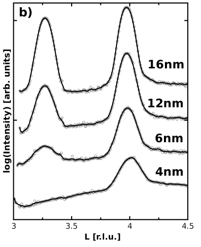
To test the hypothesis of Bi(110) and Bi(111) domain competition versus stacking, we study films grown around the transition temperature. In Fig. 3(b) we show the growth of a 16 nm thick film grown at RT where we measured a (00) CTR at several different thicknesses. The very thin 4 nm Bi film reveals a Bragg reflection for Bi(110) at L=4, but upon increasing the film thickness, the Bragg reflection for Bi(111) at L=3.3 starts developing, where for thicker films the ratio between both peaks gets more similar. Note that the center of the Bi(110) peak for the 4 nm thick film grown at RT, is slightly shifted towards higher L as compared to thicker films. This peak position corresponds to a slightly compressed average interlayer distance of 3.24Å as compared to the bulk interlayer distance of 3.27Å Sun et al. (2006); Hofmann (2006). From a quantitative Low Energy Electron Diffraction (LEED) analysis described in literatureSun et al. (2006), contracted interlayer relaxations are present within the first 4 layers of Bi(110), which can heavily contribute to the average interlayer spacing on films of only several double bilayers as is the case here. Although one might anticipate that at RT the Bi(110) film only grows up to a certain thickness and then simply transforms into a Bi(111) film, this can not be concluded from the increasing area for the peak at L=4 for increasing film thickness, revealing that the Bi(110) film continues to grow up to a significant thickness indicative for the competition between domains Bobaru et al. (2012). Realspace in-situ scanning probe microscopy (SPM) images might help to study this initial thin film growth around the transition temperature.
IV Conclusions
In summary, we have presented SXRD, CTR and XRR measurements demonstrating the controlled growth of Bi(110) and Bi(111) on an atomically well defined insulating -Al2O3(0001) substrate. At temperatures as low as 40 K, the kinetics of the film growth can be slowed down, resulting in high quality pseudo-cubic Bi(110) films, having rotational disordered domains and growing solely Bi(110) up to unanticipated thicknesses of tens of nanometers. Bringing the film to RT decreases the film-vacuum and film-substrate roughness indicative for (electronic) decoupling of the film from the substrate. By heating the Bi(110) film above 400 K a crystallographic orientation transition occurs to Bi(111).
High quality and ultrasmooth Bi(111) films can be produced by heating Bi(110) to 450 K onwards, where the roughness of the film-vacuum interface is below 1Å and the roughness between film and substrate decreases with increasing temperature. The films show a slight preferential alignment with respect to the substrate.
At temperatures around the crystallographic orientation transition (400 K), the growth of Bi(110) and Bi(111) domains are in competition. A film grown at this temperature results in the growth of thin Bi(110) domains followed by thicker Bi(111) domains.
The growth of Bi(110) structures on -Al2O3(0001) is unanticipated but will have interesting electronic propertiesHofmann (2006); Koroteev et al. (2008); Miao et al. (2015). The growth and possible coexistence of both Bi(110) and Bi(111) films on an insulating substrate is very attractive for future electronic and practical applications, as the interface between substrate and film, expected to reveal topological states, will be protected from influencing oxidation effects upon ambient exposure Tabor et al. (2011). The electronic properties of the buried interface could, e.g., be probed by second-order nonlinear optical spectroscopy Hsieh et al. (2011).
Acknowledgements.
MJ and TRJB would like to thank Helena Isern and Thomas Dufrane for their technical assistance. This work is part of the research programme of the Foundation for Fundamental Research on Matter (FOM), which is part of the Netherlands Organisation for Scientific Research (NWO).References
- Hofmann (2006) P. Hofmann, Prog. Surf. Sci. 81, 191 (2006).
- Koroteev et al. (2008) Y. M. Koroteev, G. Bihlmayer, E. V. Chulkov, and S. Bl gel, Phys. Rev. B 77, 045428 (2008).
- Xiao et al. (2012) S. Xiao, D. Wei, and X. Jin, Phys. Rev. Lett. 109, 166805 (2012).
- Yang et al. (2012) F. Yang, L. Miao, Z. F. Wang, M.-Y. Yao, F. Zhu, Y. R. Song, M.-X. Wang, J.-P. Xu, A. V. Fedorov, Z. Sun, et al., Phys. Rev. Lett. 109, 016801 (2012).
- Ando (2013) Y. Ando, Journal of the Physical Society of Japan 82, 102001 (2013).
- Sabater et al. (2013) C. Sabater, D. Gos lbez-Martnez, J. Fern ndez-Rossier, J. G. Rodrigo, C. Untiedt, and J. J. Palacios, Phys. Rev. Lett. 110, 176802 (2013).
- Aitani et al. (2014) M. Aitani, T. Hirahara, S. Ichinokura, M. Hanaduka, D. Shin, and S. Hasegawa, Phys. Rev. Lett. 113, 206802 (2014).
- Drozdov et al. (2014) I. K. Drozdov, A. Alexandradinata, S. Jeon, S. Nadj-Perge, H. Ji, R. J. Cava, B. A. Bernevig, and A. Yazdani, Nat. Phys. 10, 664 (2014).
- Aguilera et al. (2015) I. Aguilera, C. Friedrich, and S. Blügel, Phys. Rev. B 91, 125129 (2015).
- Miao et al. (2015) L. Miao, M.-Y. Yao, W. Ming, F. Zhu, C. Q. Han, Z. F. Wang, D. D. Guan, C. L. Gao, C. Liu, F. Liu, et al., Phys. Rev. B 91, 205414 (2015).
- Du et al. (2016) H. Du, X. Sun, X. Liu, X. Wu, J. Wang, M. Tian, A. Zhao, Y. Luo, J. Yang, B. Wang, et al., Nat. Commun. 7, 10814 (2016).
- Reis et al. (2016) F. Reis, G. Li, L. Dudy, M. Bauernfeind, S. Glass, W. Hanke, R. Thomale, J. Schäfer, and R. Claessen, ArXiv e-prints (2016), eprint 1608.00812.
- Song et al. (2015) F. Song, J. W. Wells, Z. Jiang, M. Saxegaard, and E. Wahlstr m, ACS Appl. Mater. Interfaces 7, 8525 (2015).
- Lu et al. (2015) Y. Lu, W. Xu, M. Zeng, G. Yao, L. Shen, M. Yang, Z. Luo, F. Pan, K. Wu, T. Das, et al., Nano Lett. 15, 80 (2015).
- Yao et al. (2016) M.-Y. Yao, F. Zhu, C. Han, D. Guan, C. Liu, D. Qian, and J.-F. Jia, Sci. Rep. 6, 21326 (2016), ISSN 2045-2322.
- Bian et al. (2016) G. Bian, Z. Wang, X.-X. Wang, C. Xu, S. Xy, T. Miller, M. Z. Hasan, F. Liu, and T. chang Chiang, ACS Nano 10, 3859 (2016).
- Liu et al. (2011) Z. Liu, C.-X. Liu, Y.-S. Wu, W.-H. Duan, F. Liu, and J. Wu, Phys. Rev. Lett. 107, 136805 (2011).
- Lima and Schmidt (2015) E. N. Lima and T. M. Schmidt, Phys. Rev. B 91, 075432 (2015).
- Tabor et al. (2011) P. Tabor, C. Keenan, S. Urazhdin, and D. Lederman, Appl. Phys. Lett. 99, 013111 (2011).
- Tanaka et al. (1999) A. Tanaka, M. Hatano, K. Takahashi, H. Sasaki, S. Suzuki, and S. Sato, Surf. Sci. 433-435, 647 (1999).
- Nagao et al. (2000) T. Nagao, T. Doi, T. Sekiguchi, and S. Hasegawa, Jpn. J. Appl. Phys. 39, 4567 (2000).
- Yaginuma et al. (2003) S. Yaginuma, T. Nagao, J. Sadowski, A. Pucci, Y. Fujikawa, and T. Sakurai, Surf. Sci. 547, L877 (2003).
- Nagao et al. (2004) T. Nagao, J. Sadowski, M. Saito, S. Yaginuma, Y. Fujikawa, T. Kogure, T. Ohno, Y. Hasegawa, S. Hasegawa, and T. Sakurai, Phys. Rev. Lett. 93, 105501 (2004).
- Kammler and von Hoegen (2005) M. Kammler and M. H. von Hoegen, Surf. Sci. 576, 56 (2005).
- M nig et al. (2005) H. M nig, J. Sun, Y. M. Koroteev, G. Bihlmayer, J. Wells, E. V. Chulkov, K. Pohl, and P. Hofmann, Phys. Rev. B 72, 085401 (2005).
- Nagao et al. (2005) T. Nagao, S. Yaginuma, M. Saito, T. Kogure, J. Sadowski, T. Ohno, S. Hasegawa, and T. Sakurai, Surf. Sci. 590, 247 (2005).
- Yaginuma et al. (2007) S. Yaginuma, T. Nagao, J. Sadowski, M. Saito, K. Nagaoka, Y. Fujikawa, T. Sakurai, and T. Nakayama, Surf. Sci. 601, 3593 (2007).
- Lükermann et al. (2014) D. Lükermann, S. Banyoudeh, C. Brand, S. Sologub, H. Pfnür, and C. Tegenkamp, Surf. Sci. 621, 82 (2014).
- Kokubo et al. (2015) I. Kokubo, Y. Yoshiike, K. Nakatsuji, and H. Hirayama, Phys. Rev. B 91, 075429 (2015).
- Scott et al. (2005) S. Scott, M. Kral, and S. Brown, Surf. Sci. 587, 175 (2005).
- McCarthy et al. (2010) D. N. McCarthy, D. Robertson, P. J. Kowalczyk, and S. A. Brown, Surf. Sci. 604, 1273 (2010).
- Kowalczyk et al. (2011) P. Kowalczyk, O. Mahapatra, D. McCarthy, W. Kozlowski, Z. Klusek, and S. Brown, Surf. Sci. 605, 659 (2011).
- Jeffrey et al. (2006) C. A. Jeffrey, S. H. Zheng, E. Bohannan, D. A. Harrington, and S. Morin, Surf. Sci. 600, 95 (2006).
- Kim et al. (2006) D.-H. Kim, S.-H. Lee, J.-K. Kim, and G.-H. Lee, Appl. Surf. Sci. 252, 3525 (2006).
- Hattab et al. (2008) H. Hattab, E. Zubkov, A. Bernhart, G. Jnawali, C. Bobisch, B. Krenzer, M. Acet, R. M ller, and M. H. von Hoegen, Thin Solid Films 516, 8227 (2008).
- Payer et al. (2008) T. Payer, I. Rajkovic, M. Ligges, D. von der Linde, M. H. von Hoegen, and F.-J. M. zu Heringdorf, Appl. Phys. Lett. 93, 093102 (2008).
- Zhang et al. (2009a) H. L. Zhang, W. Chen, X. S. Wang, J. Yuhara, and A. T. S. Wee, Appl. Surf. Sci. 256, 460 (2009a).
- Bobaru et al. (2012) S. Bobaru, É. Gaudry, M.-C. de Weerd, J. Ledieu, and V. Fournée, Phys. Rev. B 86, 214201 (2012).
- Campbell (1997) C. T. Campbell, Surf. Sci. Rep. 27, 1 (1997).
- Ernst et al. (1993) K. H. Ernst, A. Ludviksson, R. Zhang, J. Yoshihara, and C. T. Campbell, Phys. Rev. B 47, 13782 (1993).
- Campbell (1994) C. T. Campbell, J. Vac. Sci. Technol. A 12, 1825 (1994).
- Rosenfeld et al. (1993) G. Rosenfeld, R. Servaty, C. Teichert, B. Poelsema, and G. Comsa, Phys. Rev. Lett. 71, 895 (1993).
- Zhang (1997) Z. Zhang, Science 276, 377 (1997).
- Wu and Chern (2008) K. S. Wu and M. Y. Chern, Journal of Applied Physics 104, 033704 (2008).
- Balmes et al. (2009) O. Balmes, R. van Rijn, D. Wermeille, A. Resta, L. Petit, H. Isern, T. Dufrane, and R. Felici, Catal. Today 145, 220 (2009), ISSN 0920-5861.
- Okamoto (1991) H. Okamoto, Binary alloy phase diagrams (ASM International, Metals Park, 1991).
- Ponchut et al. (2011) C. Ponchut, J. M. Rigal, J. Cl ment, E. Papillon, A. Homs, and S. Petitdemange, J. Instrum. 6, C01069 (2011).
- Roobol et al. (2015) S. Roobol, W. Onderwaater, J. Drnec, R. Felici, and J. Frenken, J. Appl. Crystallogr. 48, 1324 (2015).
- Björck and Andersson (2007) M. Björck and G. Andersson, J. Appl. Crystallogr. 40, 1174 (2007).
- Takagi (1954) M. Takagi, Journal of the Physical Society of Japan 9, 359 (1954).
- Vlieg (2012) E. Vlieg, Surface and Interface Science, Volumes 1 and 2: Volume 1 - Concepts and Methods (Wiley-VCH, 2012).
- Henry et al. (1991) C. Henry, C. Chapon, C. Duriez, and S. Giorgio, Surface Science 253, 177 (1991).
- B umer et al. (1995) M. B umer, J. Libuda, A. Sandell, H.-J. Freund, G. Graw, T. Bertrams, and H. Neddermeyer, Berichte der Bunsengesellschaft f r physikalische Chemie 99, 1381 (1995).
- Zhang et al. (2009b) T. C. Zhang, Z. X. Mei, Y. Guo, Q. K. Xue, and X. L. Du, Journal of Physics D: Applied Physics 42, 065303 (2009b).
- Sun et al. (2006) J. Sun, A. Mikkelsen, M. Fuglsang Jensen, Y. M. Koroteev, G. Bihlmayer, E. V. Chulkov, D. L. Adams, P. Hofmann, and K. Pohl, Phys. Rev. B 74, 245406 (2006).
- Hsieh et al. (2011) D. Hsieh, J. W. McIver, D. H. Torchinsky, D. R. Gardner, Y. S. Lee, and N. Gedik, Phys. Rev. Lett. 106, 057401 (2011).
Supplemental Materials: Controlling the growth of Bi(110) and Bi(111) films on an insulating substrate
The Supplemental Material contains Tapping Mode Atomic Force Microscopy (TM-AFM), X-ray Photoelectron Spectroscopy (XPS) and Auger Electron Spectroscopy (AES) data of the prepared -Al2O3(0001) substrate.