Interaction-induced metallic state in graphene on hexagonal boron nitride
Abstract
The Coulomb interaction is widely known to enhance the effective mass of interacting particles and therefore tends to favor a localized state at commensurate filling. Here, we will show that, in contrast to this consensus, in a van der Waals heterostructure consisting of graphene and hexagon boron nitride (h-BN), the onsite Coulomb repulsion will at first destroy the localized state. This is due to the fact that the onsite Coulomb repulsion tends to suppress the asymmetry between neighboring carbons induced by h-BN substrate. We corroborate this surprising phenomenon by solving a tight-binding model with onsite Coulomb repulsion treated within coherent potential approximation, where hopping parameters are derived from density functional theory calculations based on the graphene/h-BN heterostructure. Our results indicate that both gapless and gapped states observed experimentally in graphene/h-BN heterostructures can be understood after a realistic value of the onsite Coulomb repulsion as well as different interlayer distances are taken into account. Finally, we propose ways to enhance the gapped state which is essential for potential application of graphene to next-generation electronics. Furthermore, we argue that band gap suppressed by many-body effect should happen in other van der Waals heterostructures.
pacs:
73.22.Pr, 71.30.+h, 73.21.Ac, 71.10.FdI Introduction
Graphene, a Dirac semimetal, is considered as a potential candidate for replacing silicon in next-generation electronics provided large gaps of order 300 K can be opened at charge neutral point. Various ways have been used to realize the gap opening Castro2007 ; Han2007 ; Elias2009 ; Ci2010 ; Hunt2013 . Among those, heterostructure consisting of two-dimensional layers of graphene and atomically flat hexagonal boron nitride (h-BN) coupled by van der Waals interactions attracts considerable interests Hunt2013 ; Xue2011 ; Britnell2012 ; Slawinska2010 ; Dean2011 ; Zhong2011 ; Gao2012 ; Amet2013 ; Tang2013 ; San-Jose075428 ; Titov2014 ; Wijk2014 ; Abergel2015 ; Slotman2015 .
While it was predicted by density functional theory (DFT) calculations that a band gap of meV can be generated in the van der Waals heterostructure Giovannetti2007 , such an insulating state was not always detected in experiments Hunt2013 ; Xue2011 ; Amet2013 ; Usachov2010 ; Roth2013 ; Chen2014 ; Sediri2015 . The discrepancy is originally ascribed to the lattice mismatch of 1.8% between graphene and h-BN which leads to moiré patterns in real space with periodicity determined by interlayer twist angle Xue2011 ; Roth2013 ; Titov2014 ; Sachs2011 . This is due to the fact that nonzero twist may give rise to a restoration of sublattice inversion symmetry on spatial average, possibly leading to a metallic state Xue2011 . However, such a metallic state is not anticipated by the noninteracting model, where a small gap persists even if lattice mismatch is involved Kindermann2012 . Also the insulating state with large band gap of around 100-300K observed experimentally Hunt2013 can not be accounted for by the noninteracting model Kindermann2012 . Then, a natural speculation arises that electronic interactions may enhance the gapped state. Indeed, various experiments indicate the importance of many-body effect in the heterostructure Dean2011 ; Chen2014 ; Dean2013 ; Shi2014 .
Recently, long-range Coulomb interactions are studied at either weak coupling limit or strong coupling limit Song2013 ; Bokdam2014 ; Jung2015 which confirm the speculation. But it is known from constrained random phase approximation calculations that the dominant onsite Coulomb repulsion is reduced by a weighted average of nonlocal interactions , resulting in an effective on-site Coulomb interaction of , where is the hopping integral of electrons between nearest neighbor carbons Schueler2013 . Therefore, it’s better to first understand the role of the effective on-site Coulomb interaction which is of intermediate strength with respect to the kinetic energy of the electrons.
In this paper, we will show that the onsite Coulomb repulsion will first suppress the band gap in the graphene/h-BN heterostructure even in the absence of lattice mismatch. The underlying physics behind the unexpected phenomenon comes from competition between two types of insulating states, namely the band insulator and the Mott insulator. As is well known, at , lattice inversion symmetry of graphene is broken by coupling to the h-BN substrate, leading to a charge imbalance between two neighboring carbons and a band gap at half-filling (i.e. the charge neutral point). However, as is switched on, the onsite Coulomb repulsion tends to localize the electrons on graphene and thus suppress the hybridization between graphene and h-BN. Therefore, the asymmetry between neighboring carbons as well as the corresponding band gap, induced by interlayer coupling, will be suppressed. Further increasing the onsite Coulomb repulsion will drive the system into the Mott insulating state.
Besides the reduction of the band gap induced by the onsite Coulomb repulsion of intermediate strength, variation of interlayer distance, which dominates the interlayer coupling between graphene and h-BN, will also strongly affect the band gap. Since large variance of the interlayer distance may exist among different measurements due to the weak van der Waals interaction and diverse experimental conditions, and the onsite Coulomb repulsion inevitably exists in real materials, our findings may provide complementary ways to understand the conundrum of why both gapped and gapless states can be observed in different experiments. We corroborate the above findings by solving a tight-binding model with onsite Coulomb repulsion treated within coherent potential approximation. The hopping parameters of the tight-binding model are derived from DFT calculations based on the graphene/h-BN heterostructure.
The paper is organized as follows. In Sec. II, we describe the details of the structure, the model, and the method we used. In Sec. III, we present our results including density of states (DOS), gap, difference in occupation numbers between neighboring carbons, total self-energy, spectral function, and phase diagram in the plane of onsite Coulomb interaction and interlayer distance. Corresponding indications of our results to experiments are also discussed in this section. We summarize our findings in Sec. IV.
II Model and Methods
II.1 Details of the heterostructures
The graphene/h-BN heterostructure we studied are composed of one h-BN monolayer and one graphene monolayer coupled by van der Waals interaction. Since the physical picture of interaction-induced reduction of the band gap is independent of lattice structure, for simplicity, we only study the van der Waals heterostructure without lattice mismatch. Further advantage to use lattice-matched structure is that, as long as the gapless state appears, it can be solely attributed to the inclusion of on-site Coulomb repulsion, since possible reduction of the band gap due to lattice mismatch is completely precluded.
There are three stable and metastable configurations of the heterostructure as shown in the insets of Fig. 4 and Fig. 7, respectively. The most stable configuration with lowest total energy is called AB-N stack where one carbon is above boron and the other centered above a h-BN hexagon as seen in the insets of Fig. 4. Two metastable configurations are given in the insets of Fig. 7, denoted by AB-B stack with one carbon over nitrogen and the other centered above a h-BN hexagon and AA stack with one carbon over boron and the other over nitrogen, respectively. Unless specified, the lattice structure we used in our paper is of AB-N stack.
II.2 Tight-binding model
The tight-binding model with onsite Coulomb interaction used to describe the graphene/h-BN heterostructure is given by
| (1) |
where () is the annihilation (creation) operator of an electron with spin at site j (i), and the density operator. denotes the summation over the sites on both graphene and h-BN while the graphene only. is the hopping integral between site i and j derived from DFT calculations and is the effective onsite Coulomb repulsion. We are interested in the half-filled case, which is corresponding to the charge neutral point in experiments. Since no long-range magnetic order is observed in the heterostructure experimentally, we focus on the paramagnetic state throughout the paper.
II.3 Details of band structure calculations
In order to determine the hopping integrals in model (1), we first perform DFT calculations within local density approximation (LDA) to obtain band structure of the graphene/h-BN heterostructure, based on projector augmented wave (PAW) method Bloechl1994 , as implemented in VASP code Kresse1993 ; Kresse1996 . The convergence of total energy with respect to K-point sampling, cutoff energies and vacuum distance between neighboring heterostructures has been carefully examined. The plane wave cutoff energy of 800 eV, a -centered K-point grid of and a vacuum distance of 17 Å are chosen when lattice constants and atomic positions of lattice-matched graphene/h-BN heterostructures are fully relaxed, with residual forces on each atom less than 1 meV/Å. Since the distances between graphene and h-BN may vary considerably among different experiments due to the weak van der Waals coupling and diverse experimental conditions, the interlayer distances will be treated as a tuning parameter while other structural parameters are fixed according to the lattice optimization. We use Monkhorst-Pack k-point meshes Monkhorst to integrate over the Brillouin zone in order to precisely determine the Fermi energy. With the parameters described above, we can reproduce the band structures of Ref. [Zhong2011, ] and Ref. [Giovannetti2007, ] where different equilibrium interlayer distances are used.
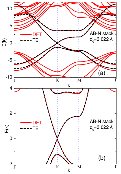
Then, the hopping integrals can be derived through transformation from Bloch space to maximally localized Wannier functions (MLWFs) basis by using wannier90 code Marzari2012 ; Mostofi . Four bands close to the Fermi energy which are mainly contributed from orbitals of two carbons of different sublattices, one nitrogen, and one boron are taken into account. Comparisons between the band structures calculated from DFT and the derived tight-binding model (1) at are shown in Fig. 1 for AB-N stack with interlayer distance of Å. Only a little differences around the point due to strong band entanglement can be seen, which will not affect the applicability of our results to the heterostructures as those states are far away from the Fermi level and therefore irrelevant to the band gap. Please note, as the noninteracting part in Eq. (1) are derived from DFT calculations, the effect of nonlocal terms of the Coulomb interactions has been implicitly incorporated in our study at the DFT level. In this paper, we will focus on the effect of the optimal onsite Coulomb interaction beyond the DFT level CommentTB .
II.4 Coherent potential approximation to the model (1)
In order to verify the above scenario of interaction-induced metallization and its relevance to graphene/h-BN heterostructure, we employ coherent potential approximation (CPA) Elliot1974 ; Jarrell2001 to solve the tight-binding model (1). By applying the alloy analogy approach Hubbard1963 , the interacting system can be viewed as a disordered alloy where an electron with spin moving on the graphene layer encounters either a potential of at a site with a spin present or without. Then, the model Hamiltonian (1) is replaced by a one-particle Hamiltonian with disorder potential which is of the form
| (2) |
where the disorder potential satisfies
| (3) |
Here, is the average occupancy of electrons on site of the graphene layer with spin . The Green’s function corresponding to the one-particle Hamiltonian has to be averaged over all possible disorder configurations. The averaging can not be performed exactly. To solve the alloy problem, the coherent potential approximation (CPA) is used Elliot1974 ; Jarrell2001 , where the disorder potential is replaced by a local complex and energy-dependent self-energy. The details of the CPA method applied to the model (1) are given in the appendix A. Here, we should stress that, although above treatment itself has a few shortcomings Gebhard1997 , it remains valuable as a computationally simple theory capable of capturing the Mott metal-insulator transition of many-body systems. For example, it successfully reproduces the phase diagram of ionic Hubbard model at half filling Hoang2010 . Moreover, the critical value of the Mott transition of RowlandsCPB2014 obtained within CPA based on a Hubbard model on honeycomb lattice at half filling is in excellent agreement with the quantum Monte Carlo simulations Assaad2013 ; Sorella2012 ; Toldin2015 and cluster dynamical mean field theory calculations Wu2010 ; Liebsch2011 ; CommentAF . More discussions about CPA can be found in Refs. [RowlandsJPCM1, ; RowlandsJPCM2, ; CommentCPA, ].
III results
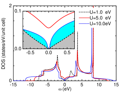
Fig. 2 shows DOSs at three different values of . Here, an equilibrium interlayer distance of Å between graphene and h-BN is used according to Ref. Zhong2011, . It is found that at a small value of eV, DOS at the Fermi level remains zero which is similar to the noninteracting case. However, when becomes larger, for example at eV, finite DOS appears at the charge neutral point, indicating emergence of an unconventional metallic state induced by onsite electronic Coulomb interaction. Further increasing will again result in a gapped state as evident from the DOS at eV.
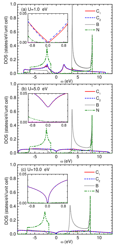
The partial DOS is presented in Fig. 3 for above three different values of . It is found that in all the cases, DOS around the Fermi level are mainly contributed from both carbons C1 and C2. The contributions of boron and nitrogen to the DOS around the Fermi level are negligibly small, compared to those of carbons. Moreover, while small difference between the DOS of C1 and C2 can be found at eV, the difference becomes indiscernible at eV and eV. This implies that the asymmetry between carbons induced by the substrate h-BN is suppressed by the onsite Coulomb repulsion. Due to the effective restoration of the inversion symmetry between carbons, the band gap induced by the asymmetry gradually vanishes, and finally an interaction-induced metallic state appears.
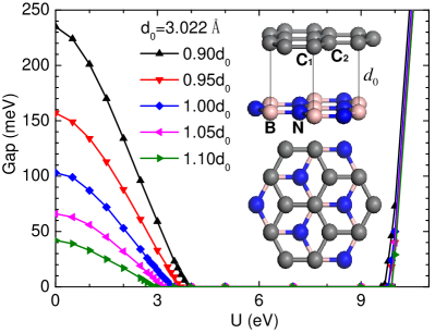
The evolution of gap size as a function of onsite Coulomb repulsion is shown in Fig. 4 for several different interlayer distances in the unit of equilibrium distance Å. While at weak interacting region, both the gap amplitudes and the critical values where the gap vanishes are strongly dependent on the interlayer distances, implying that insulating behavior in this region is dominated by coupling between graphene and h-BN, at large interacting region, those quantities remain almost unchanged, indicating that the gapped state at large is probably irrelevant to the h-BN substrate. Moreover, the strong variance of critical values at small region as a function of the interlayer distances also suggests that such an interaction-driven insulator-to-metal transition can be tuned by varying the interlayer distances between graphene and h-BN, which can be easily realized by applying out-of-plane strain to the van der Waals heterostructure.
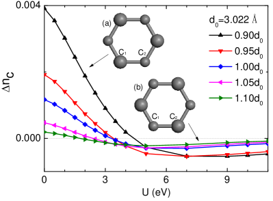
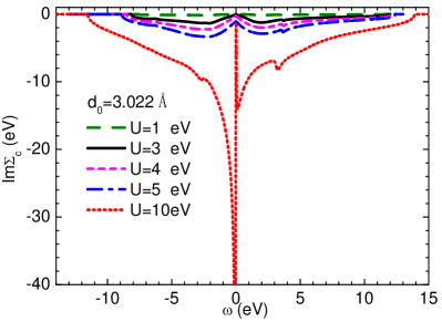
In order to reveal the nature of these two insulating states, difference of occupation number between two nearest neighbor carbons and imaginary part of total self-energy of two neighboring carbons as a function of are investigated as shown in Figs. 5 and 6, respectively. It is found that is rapidly suppressed as increases, indicating that the symmetry breaking between two neighboring carbons induced by h-BN substrate is effectively restored by the interaction continuously, leading to a reduction of gap amplitude as detected in Fig. 4. Combining the fact that the imaginary part of total self-energy at small , as displayed in Fig. 6 for or eV, vanishes in the vicinity of the charge neutral point, we conclude that in the small interacting region, it is still a band insulator where symmetry breaking dominates the gap opening. However, the situation is completely changed at large where the imaginary part of total self-energy is divergent within the gap, as seen in Fig. 6 at eV, which is a characteristic feature of a Mott insulator Georges1996 . In the intermediate range of onsite Coulomb interaction, the imaginary part of total self-energy, which will cause band broadening, becomes larger, (see or in Fig. 6), while the asymmetry between neighboring carbons becomes smaller as indicated by smaller charge difference in Fig. 5, compared to the weak interacting case. A metallic state induced by many-body interaction appears, since the small asymmetry can not provide large enough separation between broadened conduction and valence bands.
Another interesting phenomenon presented in Fig. 5 is that the difference of occupation number between neighboring carbons changes from positive to negative value, indicating a reversal from charge-richer to charge-poorer site in graphene layer for all different interlayer distances. This can be ascribed to two competing effects induced by h-BN substrate. One is the substrate-induced different local potentials between neighboring carbons, and the other is the difference of interlayer hybridizations between different carbons and the substrate. We find that the carbon above boron has higher local potential and stronger interlayer hybridization than that sitting above the center of h-BN hexagon. When is small, more electrons prefer to occupy the carbon above boron since it can gain more kinetic energy through the interlayer hopping. However, when becomes larger, the electrons in graphene get more localized, and the interlayer hoppings are suppressed. As a result, more electrons choose to occupy the carbon above the center of h-BN hexagon due to the lower local potential. Such a physical picture can also be applied to understand why a reversal from charge-richer to charge-poorer site happens at fixed value of as the interlayer distance is varied (See e.g. or eV in Fig. 5). Due to the competition between site-dependent local potentials and interlayer hybridizations, smaller interlayer distance results in larger interlayer hybridizations, and thus favors more electrons on the carbon above boron in order to gain more kinetic energy, while larger interlayer distance corresponds to weaker interlayer hybridizations and therefore less electrons on the carbon above boron due to the higher local potential.
The resulting phase diagram in the plane of interaction and interlayer distance is shown in Fig. 7. Here, we present not only the phase boundaries for most stable lattice configuration, but also those for two metastable configurations with one carbon above nitrogen and the other above the center of h-BN hexagon represented by AB-B stack, and with one carbon above boron and the other above nitrogen denoted by AA stack, respectively. We find that consecutive phase transitions from band insulator to metal and then to Mott insulator always happen despite differences in lattice configurations and the interlayer distances, indicating that the interaction-driven metallization should always occur even if lattice mismatch is taken into account.
Finally, let us discuss the implication of our results to the experimental conundrum where metallic and insulating states are both observed in different measurements Xue2011 ; Hunt2013 ; Amet2013 ; Usachov2010 ; Roth2013 ; Chen2014 ; Sediri2015 . Although it was initially argued that nonzero twist may give rise to a restoration of sublattice inversion symmetry on spatial average, leading to a metallic state Xue2011 , it was found from transport measurements that the gap remains large, e.g. of the order 200 K, even if the twist angle becomes larger than Hunt2013 . On the contrary, no gap was observed in another experiment when twist angle is larger than Woods2014 . Similar inconsistency also happens between the transport measurements and angular resolved photoemission spectroscopic studies (ARPES). From ARPES, a band with linear dispersion is observed crossing the Fermi level in the heterostructure with moiré wavelength of 9 nm, clearly indicating a metallic state Roth2013 , which is in contrast to the gapped state with same moiré wavelength reported by transport measurements Hunt2013 . These discrepancies indicate that existing explanations of the gapless or gapped state observed in different experiments based on lattice relaxations and misorientations Jung2015 ; Woods2014 can not resolve the conundrum completely.
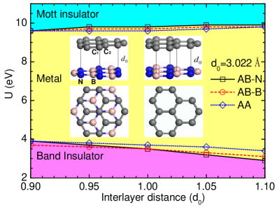
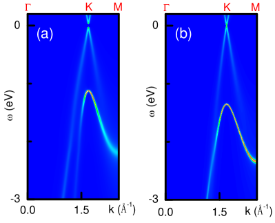
Here, according to the phase diagram, we propose a complementary way to fully understand the contradictory experiments based on the existence of onsite Coloumb interaction and the difference of interlayer distance, both of which are unavoidable in real materials, in addition to the way of considering commensurate-incommensurate phase transition Woods2014 . After the onsite Coulomb repulsion is taken into account, if we adopt eV, which is of the same value used for bilayer graphene Zhang2016 , we can find from Fig. 7 that the heterostructure is just located in the vicinity of the phase boundary between band insulator and metal. Therefore the electronic property of the heterostructure is susceptible to the variation of interlayer distance which may be considerably large among different experiments due to the weak van der Waals interaction between graphene and h-BN. In Fig. 8, we further show the spectral functions along line in the Brillouin zone at eV for two different interlayer distances of (see Fig. 8 (a)) and (see Fig. 8 (b)) with Å. While a small gap of meV is clearly visible at the distance of , nearly linear dispersive band crossing the Fermi level appears at the distance of as observed in the ARPES studies Roth2013 .
According to the phase diagram, we further propose that applying stress perpendicular to the graphene plane may open a large band gap as required for making logic transistors. Another way to enhance the gap is to put one more h-BN on top of graphene which will enhance the asymmetry between neighboring carbons and therefore lead to a large gap. Moreover, both ways will enhance the interlayer coupling and therefore lessen the lattice mismatch which is detrimental to gap opening.
IV Conclusions
In conclusion, the experimentally observed metallic state in graphene/h-BN heterostructure is always attributed to the lattice mismatch Xue2011 ; Roth2013 ; Sachs2011 ; Titov2014 , and the electronic interaction is widely believed to enhance the gapped state Hunt2013 ; Chen2014 ; Song2013 ; Bokdam2014 ; Jung2015 . However, here we show that even without lattice mismatch, dominant onsite Coulomb repulsion of realistic value will suppress the band gap due to the effective restoration of inversion symmetry between neighboring carbons. The interaction-induced insulator-to-metal transition should also happen even if lattice mismatch is involved since the phase diagrams are qualitatively the same despite different lattice configurations. Finally, we argue that the phenomenon of band gap suppressed by many-body effect should be present in other van der Waals heterostructures as long as a band gap induced by lattice asymmetry has already been opened in the noninteracting case.
V Acknowledgements
We thank W. Ku for discussions. This work is supported by National Natural Science Foundation of China (No. 11474217), Program for New Century Excellent Talents in University (NCET-13-0428), and the Program for Professor of Special Appointment (Eastern Scholar) at Shanghai Institutions of Higher Learning as well as the Scientific Research Foundation for the Returned Overseas Chinese Scholars, State Education Ministry. J.-R. is also supported by Educational Commission of Anhui Province of China (No. KJ2013B059) and Natural Science Foundation of Anhui Province (No. 1308085QA05).
Appendix A Solution of Coherent potential approximation to the model (1)
The CPA average Green’s function can be written in a matrix form
| (4) |
where is chemical potential and is a matrix obtained by applying the Fourier transformation to the model (1). and represent for self-energies on two neighboring carbons. Now all spin indices have been omitted as we are interested in the paramagnetic phase. In real space, we have
| (5) |
where the integral is over the first Brillouin zone of the sublattice and . Then a cavity Green’s function can be obtained through the Dyson equation
| (6) |
for sublattice () in graphene layer, which describes a medium with self-energy at a chosen site removed. The cavity can now be filled by a real ”impurity” with disorder potential, resulting in an impurity Green’s function
| (7) |
with impurity configurations of as defined by Eq.(3). The CPA requires
| (8) |
where the average is taken over the impurity configuration probabilities defined by Eq.( 3).
Equation (5) and (8) need to be solved self-consistently. By adjusting the chemical potential , the condition of can be satisfied for half-filled case, where
| (9) |
It is also necessary to ensure that the resulting integrated DOS for each site should be consistent with the average occupation number probabilities used in Eq.(8), so an extra loop of self-consistency should be added.
References
- (1) E. V. Castro, K. S. Novoselov, S. V. Morozov, N. M. R. Peres, J. M. B. Lopes dos Santos, J. Nilsson, F. Guinea, A. K. Geim and A. H. Castro Neto, Biased bilayer graphene: semiconductor with a gap tunable by the electric field effect, Phys. Rev. Lett. 99, 216802 (2007).
- (2) M. Y. Han, B. Özyilmaz, Y. Zhang and P. Kim, Energy band-gap engineering of graphene nanoribbons, Phys. Rev. Lett. 98, 206805 (2007).
- (3) D. C. Elias, R. R. Nair, T. M. G. Mohiuddin, S. V. Morozov, P. Blake, M. P. Halsall, A. C. Ferrari, D. W. Boukhvalov, M. I. Katsnelson, A. K. Geim and K. S. Novoselov, Control of graphene s properties by reversible dydrogenation: evidence for graphane, Science 323, 610 (2009).
- (4) L. Ci, L. Song, C. Jin, D. Jariwala, D. Wu, Y. Li, A. Srivastava, Z. F. Wang, K. Storr, L. Balicas, F. Liu and P. M. Ajayan, Atomic layers of hybridized boron nitride and graphene domains, Nat. Mater. 9, 430 (2010).
- (5) B. Hunt, J. D. Sanchez-Yamagishi, A. F. Young, M. Yankowitz, B. J. LeRoy, K. Watanabe, T. Taniguchi, P. Moon, M. Koshino, P. Jarillo-Herrero and R. C. Ashoori, Massive Dirac fermions and Hofstadter butterfly in a van der Waals heterostructure, Science 340, 1427 (2013).
- (6) J. Xue, J. Sanchez-Yamagishi, D. Bulmash, P. Jacquod, A. Deshpande, K. Watanabe, T. Taniguchi, P. Jarillo-Herrero and B. J. LeRoy, Scanning tunnelling microscopy and spectroscopy of ultraflat graphene on hexagonal boron nitride, Nat. Mater. 10, 282 (2011).
- (7) F. Amet, J. R. Williams, K. Watanabe, T. Taniguchi and D. Goldhaber-Gordon, Insulating behavior at the neutrality point in single-layer graphene, Phys. Rev. Lett. 110, 216601 (2013).
- (8) L. Britnell, R. V. Gorbachev, R. Jalil, B. D. Belle, F. Schedin, A. Mishchenko, T. Georgiou, M. I. Katsnelson, L. Eaves, S. V. Morozov, N. M. R. Peres, J. Leist, A. K. Geim, K. S. Novoselov and L. A. Ponomarenko, Field-effect tunneling transistor based on vertical graphene heterostructures, Scienece 335, 947 (2012).
- (9) J. Slawińska, I. Zasada and Z. Klusek, Energy gap tuning in graphene on hexagonal boron nitride bilayer system, Phys. Rev. B 81, 155433 (2010).
- (10) C. R. Dean, A. F. Young, P. Cadden-Zimansky, L.Wang, H. Ren, K. Watanabe, T. Taniguchi, P. Kim, J. Hone and K. L. Shepard, Multicomponent fractional quantum Hall effect in graphene, Nat. Phys. 7, 693(2011).
- (11) X. Zhong, Y. K. Yap and R. Pandey, First-principles study of strain-induced modulation of energy gaps of graphene/BN and BN bilayers, Phys. Rev. B 83, 193403(2011).
- (12) G. Gao, W. Gao, E. Cannuccia, J. Taha-Tijerina, L. Balicas, A. Mathkar, T. N. Narayanan, Z. Liu, B. K. Gupta, J. Peng, Y. Yin, A. Rubio and P. M. Ajayan, Artificially stacked atomic layers: toward new van der Waals solids, Nano Lett. 12, 3518 (2012).
- (13) S. Tang, H. Wang, Y. Zhang, A. Li, H. Xie, X. Liu, L. Liu, T. Li, F. Huang, X. Xie and M. Jiang, Precisely aligned graphene grown on hexagonal boron nitride by catalyst free chemical vapor deposition, Sci. Rep. 3, 2666 (2013).
- (14) P. San-Jose, A. Gutiérrez-Rubio, M. Sturla and F. Guinea, Spontaneous strains and gap in graphene on boron nitride, Phys. Rev. B 90, 075428 (2014).
- (15) M. Titov and M. I. Katsnelson, Metal-insulator transition in graphene on boron nitride, Phys. Rev. Lett. 113, 096801 (2014).
- (16) M. M. van Wijk, A. Schuring, M. I. Katsnelson and A. Fasolino, Moiré patterns as a probe of interplanar interactions for graphene on h-BN, Phys. Rev. Lett. 113, 135504 (2014).
- (17) D. S. L. Abergel and M. Mucha-Kruczyński, Infrared absorption of closely aligned heterostructures of monolayer and bilayer graphene with hexagonal boron nitride, Phys. Rev. B 92, 115430 (2015).
- (18) G. J. Slotman, M. M. van Wijk, P. Zhao, A. Fasolino, M. I. Katsnelson and S. Yuan, Effect of structural relaxation on the electronic structure of graphene on gexagonal boron nitride, Phys. Rev. Lett. 115, 186801 (2015).
- (19) G. Giovannetti, P. A. Khomyakov, G. Brocks, P. J. Kelly and J. van den Brink, Substrate-induced band gap in graphene on hexagonal boron nitride: Ab initio density functional calculations, Phys. Rev. B 76, 073103 (2007).
- (20) D. Usachov, V. K. Adamchuk, D. Haberer, A. Grüneis, H. Sachdev, A. B. Preobrajenski, C. Laubschat, and D. V. Vyalikh, Quasifreestanding single-layer hexagonal boron nitride as a substrate for graphene synthesis, Phys. Rev. B 82, 075415 (2010).
- (21) S. Roth, F. Matsui, T. Greber and J. Osterwalder, Chemical vapor deposition and characterization of aligned and in commensurate graphene/hexagonal boron nitride heterostack on Cu(111), Nano Lett. 13,2668 (2013).
- (22) Z. Chen, Z. Shi, W. Yang, X. Lu, Y. Lai, H. Yan, F. Wang, G. Zhang, Z. Li, Observation of an intrinsic bandgap and Landau level renormalization in graphene/boron-nitride heterostructures, Nat. Commun. 5, 4461 (2014).
- (23) H. Sediri, D. Pierucci, M. Hajlaoui, H. Henck, G. Patriarche, Y. J. Dappe, S. Yuan, B. Toury, R. Belkhou, M. G. Silly, F. Sirotti, M. Boutchich, A. Ouerghi, Atomically sharp interface in an h-BN-epitaxial graphene van der Waals heterostructure, Sci. Rep. 5, 16465 (2015).
- (24) B. Sachs, T. O. Wehling, M. I. Katsnelson and A. I. Lichtenstein, Adhesion and electronic structure of graphene on hexagonal boron nitride substrates, Phys. Rev. B 84, 195414 (2011).
- (25) M. Kindermann, Bruno Uchoa and D. L. Miller, Zero-energy modes and gate-tunable gap in graphene on hexagonal boron nitride, Phys. Rev. B 86, 115415 (2012).
- (26) C. R. Dean, L. Wang, P. Maher, C. Forsythe, F. Ghahari, Y. Gao, J. Katoch, M. Ishigami, P. Moon, M. Koshino, T. Taniguchi, K. Watanabe, K. L. Shepard, J. Hone and P. Kim, Hofstadter s butterfly and the fractal quantum Hall effect in moiré superlattices, Nature 497, 598 (2013).
- (27) Z. Shi, C. Jin, W. Yang, L. Ju, J. Horng, X. Lu, H. A. Bechtel, M. C. Martin, D. Fu, J. Wu, K. Watanabe, T. Taniguchi, Y. Zhang, X. Bai, E. Wang, G. Zhang and F. Wang, Gate-dependent pseudospin mixing in graphene/boron nitride moiré superlattices, Nat. Phys. 10, 743 (2014).
- (28) J. C. W. Song, A. V. Shytov and L. S. Levitov, Electron interactions and gap opening in graphene superlattices, Phys. Rev. Lett. 111, 266801 (2013).
- (29) M. Bokdam, T. Amlaki, G. Brocks and P. J. Kelly, Band gaps in incommensurable graphene on hexagonal boron nitride, Phys. Rev. B 89, 201404(R) (2014).
- (30) J. Jung, A. M. DaSilva, A. H. MacDonald and S. Adam, Orgin of band gaps in graphene on hexagonal boron nitride, Nat. Commun. 6, 6308 (2015).
- (31) M. Schüler, M. Rösner, T. O. Wehling, A. I. Lichtenstein, and M. I. Katsnelson, Optimal Hubbard models for materials with nonlocal Coulomb interactions:graphene, silicene, and benzene, Phys. Rev. Lett. 111, 036601 (2013).
- (32) P. E. Blöchl, Projector augmented-wave method, Phys. Rev. B 50, 17953 (1993).
- (33) G. Kresse and J. Hafner, Ab initio molecular dynamics for liquid metals, Phys. Rev. B 47, 558 (1993).
- (34) G.Kresse and J.Furthmüller, Efficient iterative schemes for ab initio total-energy calculations using a plane-wave basis set, Phys. Rev. B 54, 11169 (1996).
- (35) H. J. Monkhorst and J .D. Pack, Special points for Brillouin-zone integrations, Phys. Rev. B 13, 5188 (1976).
- (36) N. Marzari, A. A. Mostofi, J. R. Yates, I. Souza, D. Vanderbilt, Maximally localized Wannier functions: Theory and applications, Rev. Mod. Phys. 84, 1419 (2012).
- (37) A. A. Mostofi, J. R. Yates, Y. S. Lee, I. Souza, D. Vanderbilt and N. Marzari, wannier90: A Tool for Obtaining Maximally-Localised Wannier Functions, Comput. Phys. Commun. 178, 685 (2008).
- (38) Besides the semi-local approximations to the exchanges and correlations, density functional theory calculations (DFT) have also included the Hartree term of the nonlocal Coulomb interaction. Therefore, we mentioned that the effect of nonlocal terms of the Coulomb interactions has been implicitly incorporated in our study at the DFT level. However, the exact exchange term, i.e., the Fock term, is not involved in our DFT calculations based on local density approximation. As we know, the exact exchange term will enhance the band gap. While this will eventually lead to a shift of phase boundary, the overall phase diagram remains qualitatively unchanged.
- (39) R. J. Elliot, J. A. Krumhansk and P. L. Leath, The theory and properties of randomly disordered crystals and related physical systems, Rev. Mod. Phys. 46, 465 (1974).
- (40) M. Jarrell and H. R. Krishnamurthy, Systematic and causal corrections to the coherent potential approximation, Phys. Rev. B 63, 125102 (2001).
- (41) J. Hubbard, Electron correlations in narrow energy bands, Proc. Roy. Soc. (London) A276, 238 (1963).
- (42) F. Gebhard, The Mott Metal-Insulator Transition: Models and Methods, (New York: Spinger), (1997).
- (43) A. T. Hoang, Metal-insulator transitions in the half-filled ionic Hubbard model, J. Phys.: Condens. Matter 22, 095602 (2010).
- (44) D. A. Rowlands, Y.-Z. Zhang, Disappearance of the Dirac cone in silicene due to the presence of an electric field, Chin. Phys. B 23, 037101 (2014).
- (45) F. F. Assaad, I. F. Herbut, Pinning the Order: The Nature of Quantum Criticality in the Hubbard Model on Honeycomb Lattice, Phys. Rev. X 3, 031010 (2013).
- (46) S. Sorella, Y. Otsuka, S. Yunoki, Absence of a Spin Liquid Phase in the Hubbard Model on the Honeycomb Lattice, Scientific Reports 2, 992 (2012).
- (47) F. P. Toldin, M. Hohenadler, F. F. Assaad, Fermionic quantum criticality in honeycomb and -flux Hubbard models: Finite-size scaling of renormalization-group-invariant observables from quantum Monte Carlo, Phys. Rev. B 91, 165108 (2015).
- (48) W. Wu, Y.-H. Chen, H.-S. Tao, N.-H. Tong, W.-M. Liu, Interacting Dirac fermions on honeycomb lattice, Phys. Rev. B 82, 245102 (2010).
- (49) A. Liebsch, Correlated Dirac fermions on the honeycomb lattice studied within cluster dynamical mean field theory, Phys. Rev. B 83, 035113 (2011).
- (50) The critical value of the metal-insulator transition of the Hubbard model on honeycomb lattice obtained within antiferromagnetic state Assaad2013 ; Sorella2012 ; Toldin2015 is consistent with that within paramagnetic state Wu2010 ; Liebsch2011 , indicating that our conclusion should remain unchanged even if long-range antiferromagnetic order were taken into account.
- (51) D. A. Rowlands, Y.-Z. Zhang, Inclusion of intersite spatial correlations in the alloy analogy approach to the half-filled ionic Hubbard model, J. Phys.: Condens. Matter 26, 274201 (2014).
- (52) D. A. Rowlands, Y.-Z. Zhang, Dynamical nonlocal coherent-potential approximation for itinerant electron magnetism, J. Phys.: Condens. Matter 26, 475602 (2014).
- (53) Though the coherent potential approximation (CPA) can successfully capture the metal-insulator transition, here we would like to make a brief summary of its limitations which are discussed detailedly in Refs. [RowlandsJPCM1, ; RowlandsJPCM2, ]; the first is the inability to describe magnetism, and the second is the incapability to determine the nature of the metallic state. However, these limitations will not affect the applicability of CPA to our current research, since we are only interested in the nontrivial issue of whether there is interaction-induced insulator-metal transition possibly happening in graphene on hexagonal boron nitride where no long-range magnetic order is observed. Please note, it is not our attempt to solve the minor details of whether the metal-insulator transition is accompanied by the antiferromagnetic phase transition or whether the metallic state is a Fermi liquid, a non-Fermi liquid, or a marginal Fermi liquid.
- (54) A. Georges, G. Kotliar, W. Krauth, M. J. Rozenberg, Dynamical mean-field theory of strongly correlated fermion systems and the limit of infinite dimensions, Rev. Mod. Phys. 68, 13 (1996).
- (55) C. R. Woods, L. Britnell, A. Eckmann, R. S. Ma, J. C. Lu, H. M. Guo, X. Lin, G. L. Yu, Y. Cao, R. V. Gorbachev, A. V. Kretinin, J. Park, L. A. Ponomarenko, M. I. Katsnelson, Yu. N. Gornostyrev, K.Watanabe, T. Taniguchi, C. Casiraghi, H-J. Gao, A. K. Geim, K. S. Novoselov, Commensurate-incommensurate transition in graphene on hexagonal boron nitride, Nat. Phys. 10, 451 (2014).
- (56) J. Xu, Z. Song, H. Lin and Y. Zhang, Gate-induced gap in bilayer graphene suppressed by Coulomb repulsion, Phys. Rev. B 93, 035109 (2016).