Corresponding author. ]Tel.: +7 831 4623304;
E-mail address: maksimova.galina@mail.ru (G.M. Maksimova)
Spin- and valley-dependent Goos-Hänchen effect in silicene and gapped graphene structures
Abstract
We investigate the Goos-Hänchen shift for ballistic electrons (i) reflected from a step-like inhomogeneity of the potential energy and (or) effective mass, and (ii) transmitted through a ferromagnetic barrier region in monolayer silicene or gapped graphene. For the electrons reflected from a single interface we found that the Goos-Hänchen shift is valley-polarized for gapped graphene structure, and valley- and spin-polarized for silicene due to the spin-valley coupling. Incontrast, for example, to gapless graphene the lateral beam shift in gapped structures occurs not only in the case of total, but also of partial, reflection, i.e. at the angles smaller than the critical angle of total reflection. We have also demonstrated that the valley- and spin-polarized displacement of the electron beam, transmitted through a ferromagnetic silicene barrier, resonantly depends on the barrier width. The resonant values of the displacement can be controlled by adjusting the electric potential, the external perpendicular electric field, and the exchange field induced by an insulating ferromagnetic substrate.
INTRODUCTION
It is well-known that a light beam incident on an interface of two dielectric media undergoes a lateral displacement under the condition of total internal reflection. This phenomenon was first observed in the experiment by Goos and Hänchen GH , and named the Goos-Hänchen (GH) shift. Theoretical explanation of the effect was given by Artmann who used the stationary phase method Art . During the last decades, analogies of the spatial GH shift have been widely studied in acoustics, electronics, atomic optics, and particle physics. Interest in this phenomenon does not weaken up to now Ign ; Haan ; Chen1 ; Duan ; Savch ; Zhou ; Chen2 ; Yuan ; Been ; Lu ; Song1 . In particular, many works have been devoted to the electronic analog of the GH effect in semiconductor and graphene-based nanostructures with like-Dirac Hamiltonian (see Ref. Chen3 and references therein for review). The characteristic value of the GH displacement for Dirac electrons at a total reflection is of the order of a Fermi wavelength . Therefore, detecting the displacement is not a simple problem. However, as has been shown, the lateral shift for the electron beam tunneling through a single barrier structure can be enhanced by the transmission resonances when the incidence angle is less than the critical angle of total reflection Lu ; Chen4 ; Chen5 . Even greater effect arises in double-barrier structures (DBS). The GH effect of Dirac fermions in graphene DBSs was investigated by Song et al. Song1 . The authors found that at certain parameters the magnitude of the shift for transmitted electron beam increases dramatically and can reach values of the order of which are much greater than the maximum magnitude in the corresponding single barrier structure Chen5 . It is remarkable that such giant GH shifts occur within the transmission gap and, as the authors suggest, their appearance is due to the quasibound states in the DBS. Such states are formed by the evanescent waves in the barriers. Indeed, as shown in Ref. Song1 , significant difference in the phase shifts between the central and adjacent plane waves in the wave packets arises when the parameters of central plane wave correspond to the quasibound state. The ability of a control of the GH shift by electric and magnetic barriers or by strain-induced pseudo-magnetic fields can be used for design variety of devices such as spin beam splitter Lu ; Zhang1 ; Song2 or valley beam splitter in graphene Zhai ; Zhang2 ; Wang . However, the use of graphene in various device applications strikes on a strong restriction consisting in a lack of the energy gap in the electronic spectrum. This problem does not arise for some other promising two-dimensional materials, such as h-BN, dichalcogenides of transition metals, silicene and germanene having a honeycomb structure in -plane similarly to graphene. Silicene has been predicted by Takeda and Shiraishi Takeda and investigated in detail in Ref. Guzm . There are two significant distinctions between silicene and graphene. First, it is a strong spin-orbit coupling (SOC) resulting in a band gap in silicene spectrum, which is about meV Liu1 ; Liu2 . Second, this is a buckled structure with two different sublattice planes separated by the distance nm. This, in turn, makes it possible to control the energy gap in silicene by applying an external perpendicular electric field Ni ; Drum ; Ezawa1 ; Cai . Germanene has similar properties.
In this paper we investigate the GH shift for Dirac fermions in silicene both at the total reflection and transmission through a barrier in the presence of inhomogeneous electric field, tunable potential and exchange field . The results also can be applied to graphene structures, including the gapped graphene modification.
The effective low-energy Hamiltonian in silicene for Dirac electrons with spin in the vicinity of the and points is
| (1) |
Here m/s is the Fermi velocity, are the Pauli matrices in the sublattice space, is the identity matrix, is the barrier potential induced by the gate voltage. The second term in Eq. (1), depending on the valley index and spin, describes the bandgap caused by the intrinsic SOC with strength meV which is controlled by the external perpendicular electric field . The parameter nm. For germanene meV and nm Liu2 . The exchange field is assumed to be originated from the insulating ferromagnetic substrate. In particular, it has been analyzed theoretically if ferromagnetic insulator EuO is capable of creating spin splitting in graphene of the order of meV Haug . In Ref. Yang Yang et al. reported on the first-principles calculations of magnetic properties in graphene caused by the interaction of graphene with nearby europium oxide. Specifically, they found that large exchange-splitting band gap of about meV appears in the Dirac point. The influence of exchange field on spin and valley transport through arrays of silicene barriers has been studied in several works Yok ; Sood ; Niu ; Varg ; Miss . Note, that in contrast to Refs Sood ; Ezawa2 we consider exchange fields which are the same for both sublattices. In the calculations we use the value meV.
I Goos-Hänchen shift for the electron beam reflected from a single interface
Suppose that the sample is non-ferromagnetic, i.e. everywhere. The wave functions in the two different regions I (at ) and II (at ) can be written in terms of incident, reflected and evanescent waves with the incidence angle . In the region I, where and , we have
| (2) |
where , are the components of the electron wave vector with , , , and is the reflection amplitude. When the angle exceeds the critical angle for total reflection
| (3) |
the evanescent solution in the second region (in which and ) can be written as
| (4) |
where , and is the transmission amplitude. Hereafter , and are “measured” in units of . Matching the wave functions at the interface , we obtain the coefficients and , where
| (7) |
To find the GH shift we use the stationary phase method discussed in detail with regard to graphene in a number of works (see, e.g., Refs Been ; Song1 ; Chen3 ; Chen5 ). However, due to the presence of the gap, the expression for the GH displacement of the reflected beam is not equivalent to the one obtained earlier for a gapless graphene. Assume that the wave functions of the incident and reflected beams have the form
| (8) |
| (9) |
where the quantities , , and are defined by Eqs (2) and (7), and is the angular spectrum distribution assumed to be of Gaussian shape around the central wave vector . For a well-collimated beam the position of the maximum of the upper or lower component of the wave function is determined by the requirement that the phase of this component be extremal as a function of at . Thus, at the interface the location of the upper () and lower () components of the incident wave function are: , . Similarly, for the reflected wave packet: and , where () is the phase of the reflection amplitude (Eq. (7)). The shifts of the upper and lower components, respectively, are given by
| (12) |
The average GH displacement is determined by both components. However, unlike a gapless graphene, their contributions to the wave packet are different: for the upper component, and for the lower one. Therefore, the expression for the GH shift in silicene (or gapped graphene) is determined by the formula:
| (13) |
For gapless graphene and Been . After straightforward calculations we obtain the GH shift in total reflection (13) in the following form:
| (14) |
where , , and for given values of the electric field in both half-spaces depend on the product of spin and valley indices. The values of and are taken at . At appropriate choice of parameters the resulting expression (14) can be used for graphene. In the latter case is the onsite potential difference between A and B sublattices, which does not depend on valley and spin indices, so that the GH displacements of the electrons belonging to the valleys and satisfy the simple relation
| (15) |
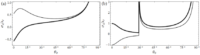
In particular, when everywhere, we get the results of Ref. Been for gapless graphene. Fig. 1(a) illustrates the dependence of the GH shift for gapped graphene at . Here, the parameters are chosen so that the condition for total internal reflection is satisfied at all angles . For normal incidence, the displacement of electrons belonging to and valleys differs only in sign: . As the angle of incidence increases, this difference reduces, in fact, to zero. Our consideration shows that the existence of the gap in the graphene spectrum results in the valley-dependent GH effect. It is not so if the wave packet is reflected from the boundary of the p-n junction in gapless graphene Been or from the sharp heterojunction separating the gapless and gapped graphene fractions. In the latter case, the GH shifts defined by the simple expression
| (16) |
In addition, we found that in other gapped structures the lateral beam shift takes place not only in the case of total but also at partial reflection (when ) and has the form:
| (17) |
Figure 1(b) shows the angular dependence of the GH shifts for the valley-polarized electron beams reflected from the interface of gapped ( meV) and gapless () graphene regions. Expression (17) describes this dependence within . At , the displacements are computed using Eq. (14).
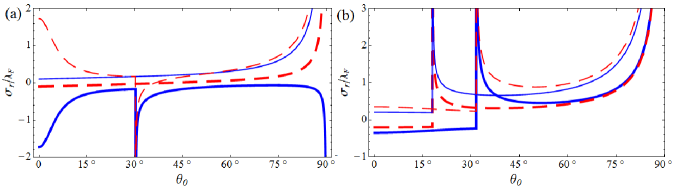
In silicene the picture of the GH shifts becomes more complicated due to their dependence not only on the valley index but also on the spin direction (Fig. 2). Therewith, the critical angle (3) depends on the product of the spin () and valley () indices. Thus, there are two critical angles corresponding to (Fig. 2(b)). In particular, for a certain value of the product , we can so choose the parameters of the structure that the condition of total internal reflection will be satisfied at all angles . Fig. 2(b) illustrates such a case for .
When reflecting from a single interface, the value of the lateral displacement (which can be positive or negative) is of the order of several Fermi wavelengths. However, in order to detect the valley-dependent (or spin-valley-dependent) GH shift, the difference of the displacements for and valleys should be greater than the longitudinal width of the initial electron beam, which is about Fermi wavelengths Song1 . A stronger effect, i.e. significant increase of the shift magnitude, can be achieved for the electronic beam passing through the single- or double-barrier structures Song1 ; Chen5 .
II Goos-Hänchen-like shift for Dirac fermions transmitted through a single barrier
The lateral displacement of electron beams tunneling through a ferromagnetic barrier structure formed by an electrostatic potential and exchange field in silicene (or graphene) sheet is defined by the transmission amplitude of the plane-wave solution of the Dirac equation
| (18) |
Here can be found from the relation Az
| (19) |
where and are the wave vectors inside and outside the barrier, respectively, , and is the width of the potential barrier. The gap parameters and are defined by the values of the electric field and in the corresponding regions (in silicene). In the case where the incident beam is well collimated around some transverse wave vector , the GH shift for the transmitted beam is Song1 ; Chen5 . When the incidence angle is less than the critical angle for the total reflection (Eq. (3)), we obtain from Eq. (19):
| (20) |
where wave vectors , are taken at , and
| (21) |
Note, that angles of incidence exceeding the critical value , the lateral shift can be obtained from these equations by replacing , where .
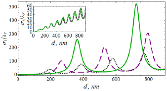
As follows from equations (20), (21) the GH shift for the electrons, transmitted through the non-ferromagnetic barrier in graphene is the same for both valleys and both values of spin. In the absence of perpendicular electric field this result takes place also for silicene. However, applied electric field leads to a GH shift, depending on the spin-valley index (Fig. 3). In the case of propagating beam (i.e. at ) the dependence of the lateral displacement on the barrier width has a pronounced resonant character. The resonance widths , at which the barrier is transparent, are determined from the relations . For such a barrier structure we immediately find from Eq. (19) the resonant values of the GH shifts
| (22) |
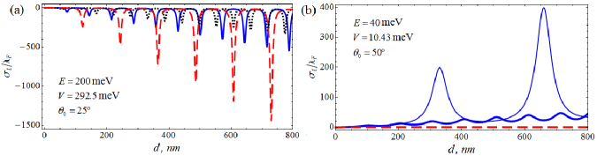
which can be modulated by the potential barrier height and the induced gaps and . Thus, as follows from Eq. (22), the increase of the gap outside the barrier suppresses the effect, i.e. leads to a decrease in the magnitude of . At the same time, comparison of the curves in Fig. 3 corresponding to different values of shows that the absolute value of the shift increases with increasing the gap parameter in the barrier which is consistent with the results of Ref. Chen5 . Thus, for spin-valley polarization , the electric field in the barrier region reduces the effective gap parameter and, consequently, the value of approximately by the order of magnitude compared to its value at (see insert in Fig. 3).
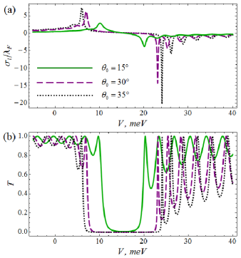
In Fig. 4 we present (a) the GH shift and (b) transmission probability (Eq. (19)) as function of the barrier height at different angles of incidence. We see that outside the transmission gap the GH shift exhibits a resonance structure. The resonance values of the potential are defined as with . Thus, for a given (), there are two resonances located to the right () and left () from the transmission gap (Fig. 4(b)), and corresponding to the Klein and classical tunneling respectively. Resonant displacement is obtained from Eq. (22), and has the form
| (23) |
This expression clearly demonstrates that, (i) the magnitude of the displacement decreases rapidly with increasing resonance number , and (ii) the GH shift is negative for Klein tunneling. In this case, increase of the gap value results in the increase of the -th resonance amplitude. Increase of the angle of incidence leads to the same effect (Fig. 4(a)). Not so obvious, but can be shown, that in the classical case () lateral shifts become positive and, as follows from Eq. (20), at given the magnitude of Klein displacement is greater than (Fig. 4(a)). Inside the transmission gap that corresponds to the evanescent solutions the GH shift is of the order of electron wavelength similarly to the case of the GH effect at a single graphene interface. We also examined modulation of the GH shift depending on energy of the incident beam. Corresponding dependence is similar to the one discussed above but the Klein and classical zones (and, accordingly, the signs of the GH shifts) are now interchanged.
For electrons transmitted through the ferromagnetic region ( at ) the height of the effective potential barrier turns out to be spin-dependent. This influences the transport properties of both silicene Yok ; Sood ; Niu ; Varg ; Miss and graphene Haug . In particular, the GH displacement becomes spin-polarized for graphene (Fig. 5(a)) and, due to the correlation between the valley and spin degrees of freedom, spin-and-valley-polarized for silicene (Fig.5(b)). The GH shifts obtained above can be positive or negative depending on the ratio between the electron energy and barrier height . Thus, all curves in Fig. 5(a) correspond to the case of Klein tunneling () through a ferromagnetic barrier region in gapped graphene. In this case is negative for both spin channels and, as follows from Eq. (22), the magnitude of the shift in the -th resonance increases with decreasing the difference between and . The GH shifts for classical tunneling () in silicene are shown in Fig. 5(b) by solid lines for both valleys with . In this case the barrier heights for electrons belonging to different valleys are equivalent, but the magnitudes of the gap inside the barrier differ: , . Accordingly, the electrons from the -valley have greater displacement than the -polarized electrons. For the parameters used, electrons with the spin-down projections in both valleys are described by the evanescent waves inside the barrier which leads to the suppression the GH effect (red dashed line in Fig. 5(b)).
SUMMARY
We have investigated the GH shifts for Dirac fermions totally reflected from the profile of the potential energy and effective mass as well as transmitted through a ferromagnetic barrier region in silicene and gapped graphene. We have shown that the presence of the gap in the graphene spectrum results in the valley-dependent GH effect in total reflection. In silicene the lateral displacement of the reflected beam also depends on the spin direction due to the coupling between valley and spin degrees of freedom. It was also found that in gapped structures the lateral beam shift occurs not only in the case of total, but also in partial reflection (Eq. (17)). For the electrons, transmitted through the barrier region the GH shift can be enhanced by the transmission resonances. The resonant values of the displacement depend on the incidence angle and the electron energy as well as on the structure characteristics such as the barrier height and gap. In particular, our results show that the GH shift increases (decreases) with increasing the gap inside (outside) the barrier. We have also demonstrated that for a normal/ferromagnetic/normal silicene junction the GH shift is valley- and spin-polarized. The obtained results can also be applicable to other two-dimensional hexagonal crystals, such as germanene or monolayers of MoS2 and other group VI dichalcogenides, which have two inequivalent valleys and two inequivalent lattices.
ACKNOWLEDGMENTS
This work was supported by the Russian Foundation for Basic Research (Grant No. -mola). E.S.A. acknowledges support by the “Dynasty” Foundation.
References
- (1) F. Goos, H. Hänchen, Ann. Phys. 1 (1947) 333; 5 (1949) 251.
- (2) K.V. Artmann, Ann. Phys. 2 (1948) 87.
- (3) V.K. Ignatovich, Phys. Lett. A 322 (2004) 36.
- (4) V.-O. de Haan, J. Plomp, T.M. Rekveldt, W.H. Kraan, Ad A. van Well, R.M. Dalgliesh, S. Langridge, Phys. Rev. Lett. 104 (2010) 010401.
- (5) X. Chen, C.-F. Li, Phys. Rev. E 69 (2004) 066617.
- (6) Z. Duan, L. Hu, X.X. Xu, C. Liu, Opt. Exp. 22 (2014) 17679.
- (7) A.S. Savchenko, A.S. Tarasenko, S.V. Tarasenko, V.G. Shavrov, JETP Lett. 102:6 (2015) 380.
- (8) L. Zhou, J.-L. Qin, Z. Lan, G. Dong, W. Zhang, Phys. Rev. A 91 (2015) 031603.
- (9) X. Chen, X.-J. Lu, Y. Wang, C.-F. Li, Phys. Rev. B 83 (2011) 195409.
- (10) L. Yuan, L.-L. Xiang, Y.-H. Kong, M.-W. Lu, Z.-J. Lan, A.-H. Zeng, Z.-Y. Wang, Eur. Phys. J. B 85 (2012) 1434.
- (11) C.W.J. Beenakker, R.A. Sepkhanov, A.R. Akhmerov, J. Tworzydło, Phys. Rev. Lett. 102 (2009) 146804.
- (12) M.-W. Lu, G.-L. Zhang, S.-Y. Chen, J. Appl. Phys. 112 (2012) 014309.
- (13) Y. Song, H.-C. Wu, Y. Guo, Appl. Phys. Lett. 100 (2012) 253116
- (14) X. Chen, X.-J. Lu, Y. Ban, C.-F Li, J. Opt. 15 (2013) 033001.
- (15) X. Chen, C.-F. Li, Y. Ban, Phys. Lett. A 354 (2006) 161.
- (16) X. Chen, J.-W. Tao, Y. Ban, Eur. Phys. J. B 79 (2011) 203.
- (17) Q. Zhang and K.S. Chan, Appl. Phys. Lett. 105 (2014) 212408.
- (18) Y. Song and G. Dai, Appl. Phys. Lett. 106 (2015) 223104.
- (19) F. Zhai, Y.-L. Ma, K. Chang, New J. Phys. 13 (2011) 083029.
- (20) Q. Zhao and K.S. Chan, RSC Advances 5 (2015) 8371.
- (21) J. Wang, M. Long, W.-S. Zhao, Y. Hu, G. Wang, and K.S. Chan, J. Phys.: Condens. Matter 28 (2016) 285302.
- (22) K. Takeda, K. Shiraishi, Phys. Rev. B 50 (1994) 14916.
- (23) G.G. Guzmán-Verri, L.C. Lew Yan Voon, Phys. Rev. B 76 (2007) 075131.
- (24) C.-C Liu, W. Feng, Y. Yao, Phys. Rev. Lett. 107 (2011) 076802.
- (25) C.-C. Liu, H. Jiang, Y. Yao, Phys. Rev. B 84 (2011) 195430.
- (26) Z. Ni, Q. Liu, K. Tang, J. Zheng, J. Zhou, R. Qin, Z. Gao, D. Yu, J. Lu, Nano Lett. 12 (2012) 113.
- (27) N.D. Drummond, V. Zólyomi, V.I. Fal ko, Phys. Rev. B 85 (2012) 075423.
- (28) M. Ezawa, New J. Phys. 14 (2012) 033003.
- (29) Y. Cai, C.-P. Chuu, C.M. Wei, M.Y. Chou, Phys. Rev. B 88 (2013) 245408.
- (30) H. Haugen, D. Huertas-Hernando, A. Brataas, Phys. Rev. B 77 (2008) 115406.
- (31) H.X. Yang, A. Hallal, D. Terrade, X. Wainta, S. Roche, and M. Chshiev, Phys. Rev. Lett. 110 (2013) 046603.
- (32) T. Yokoyama, Phys. Rev. B 87 (2013) 241409.
- (33) B. Soodchomshom, J. Appl. Phys. 115 (2014) 023706.
- (34) Z.P. Niu and S. Dong, Appl. Phys. Lett. 104 (2014) 202401.
- (35) V. Vargiamidis and P. Vasilopoulos, Appl. Phys. Lett. 105 (2014) 223105; J. Appl. Phys. 117 (2015) 094305.
- (36) N. Missault, P. Vasilopoulos, V. Vargiamidis, F.M. Peeters, B. Van Duppen, Phys. Rev. B 92 (2015) 195423.
- (37) M. Ezawa, Phys. Rev. B 87 (2013) 155415.
- (38) E.S. Azarova, G.M. Maksimova, Physica E 74 (2015) 1.