Determination of hole -factor in InAs/InGaAs/InAlAs quantum wells by magneto-photoluminescence studies
Abstract
Circularly-polarized magneto-photoluminescence (magneto-PL) technique has been applied to investigate Zeeman effect in InAs/InGaAs/InAlAs quantum wells (QWs) in Faraday geometry. Structures with different thickness of the QW barriers have been studied in magnetic field parallel and tilted with respect to the sample normal. Effective electron-hole -factor has been found by measurement of splitting of polarized magneto-PL lines. Landé factors of electrons have been calculated using the 14-band method and -factor of holes was determined by subtracting the calculated contribution of the electrons from the effective electron-hole -factor. Anisotropy of the hole -factor has been studied applying tilted magnetic field.
pacs:
xxxI Introduction
Heterostructures based on InAs possess series of unique properties caused by a narrow bandgap. These properties include high carrier mobility and a strong spin-orbit interaction making the system a promising candidate for high frequency electronics, optoelectronics and spintronics application. One of the most interesting objects in this area are type-I quantum wells (QWs) based on a InAs/InGaAs/InAlAs two-step bandgap engineering, where In content can be varied from 30 to 80% Inoue1991 . Such structures exhibit bright photoluminiscence in mid-infrared range Tournie1992 ; Terent'ev2014 demonstrate high-mobility two-dimensional electron gas Richter2000 ; Heyn2003 ; Moller2003 ; Hirmer2011 , pronounced spin-dependent optical Tsumura2006 ; Terent'ev2014 ; Terent'ev2015 and transport Hu2003 ; Nitta2003 ; Wurstbauer2009 ; Wurstbauer2010 ; Ganichev2009 ; Olbrich2012 phenomena. Determination of Landé factors of both types of the carriers is the cornerstone for the studies of spin-related phenomena. As for InAs QWs, electron -factor in this type of heterostructures is well-studied by different techniques. To date, reported values of electron -factor obtained by magneto-transport and terahertz experiments range from = -3 to = -9 depending on In content in QW barrier Moller2003 ; Wurstbauer2009 ; Nitta2003 . Moreover, experimentally obtained Landé factors are consistent with the values calculated in the framework of method.
In contrast to electrons, determination of the hole -factor is still a challenging task. There are no available experimental data as well as reliable theoretical calculations. The picture becomes even more intriguing in light of the previous magneto-optical experiments Tsumura2006 ; Terent'ev2014 . They indicate surprisingly small magnitude of the effective electron-hole -factor which is the difference between and .
Here we report on studies of InAs/In0.75Ga0.25As/In0.75Al0.25As QW structures by polarization-resolved magneto-PL, which enables direct measurement of effective electron-hole -factor. We have determined Landé factor of holes combining obtained experimental data with theoretical calculations of an electron contribution. We have obtained the dependence of electron and hole -factors on QW barrier width. We have investigated anisotropy of the hole -factor in tilted magnetic field, and shown that the values of in tilted magnetic field are in agreement with prediction of close-to-zero hole Zeeman splitting in magnetic field lying in QW plane.
II Samples and Experimental technique
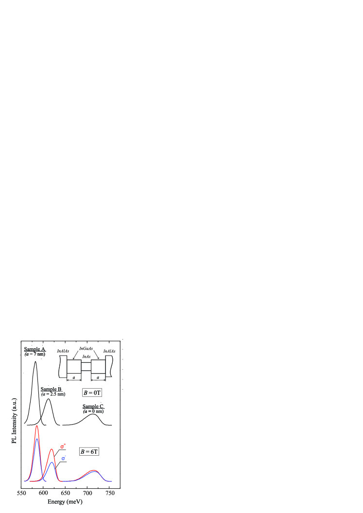
Experimental samples were fabricated by molecular beam epitaxy onto a fully relaxed InxAl1-xAs/(001)GaAs graded buffer Capotondi2005 ; Terent'ev2014 with a stepwise increase of the In content ( = 0.05 to = 0.75) over 1 m. The structure of QW is sketched in the inset of Fig. 1. An In0.75Ga0.25As quantum size part embedded in between In0.75Al0.25As layers features a symmetrically inserted and compressively strained InAs QW of 4 nm. A set of samples with the different thickness of In0.75Ga0.25As barrier was grown, where is set to 7, 2.5 and 0 nm. The corresponding structures are labeled A, B and C.
PL was excited by emission of a laser diode operating in the cw mode at wavelength nm and detected with a Fourier Transform Infrared (FTIR) spectrometer. The laser beam was focused to a 1-mm diameter spot on the sample. The excitation intensity was 100 mW. An external magnetic field up to 6 T was applied perpendicularly to the wafer or was inclined at an angle of 40∘ to the direction of sample growth. PL emission having wave vector directed along magnetic field was detected (Faraday geometry). The sample temperature was kept as low as 2 K. Right- and left-handed circular polarized emission spectra were recorded applying a quarter wave ZnSe Fresnel rhomb Ganichev1 ; Ganichev2 .
III Experimental results
Bright PL was detected from all the samples. Its contour is close to Gaussian function and slightly asymmetric being broadened at low energy slope, see Fig. 1. PL peak energy takes the value of 582.6 meV, 616.5 meV and 713.6 meV in structures A, B and C, respectively. So PL peak energy increases with decrease of InGaAs barrier width. Emission intensity also varies in samples with different barrier width and decays with its reduction. Both trends correlate with increase of PL peak full width at half maximum (FWHM) that takes the value of 18, 22 and 40 meV, in samples A, B and C, respectively. Application of external magnetic field in direction perpendicular to QW plane results in substantial changes in the PL spectrum. It experiences magnetic-field-induced splitting into circular polarized components, which is different in structures A, B and C, see Fig. 2. Similar to PL peak energy and FWHM, the splitting depends on InGaAs barrier width. It is extremely small in structure A with the largest InGaAs barrier but is well-pronounced in sample C, where this layer is absent, taking intermediate value in structure B. Interestingly, the splitting is a non-linear function of the magnetic field and its dependence on magnetic field is different in all three samples, see Fig. 2. Note that minimal circular polarization of PL emission was detected in structure C while it possesses the largest splitting. The inclination of the magnetic field used for the analisis of anisotropy critically diminishes the splitting of a magneto-PL peak in samples B and C, however does not affect it in sample A, see Fig. 2.
Besides the splitting of the PL contour into circular-polarized components, emission spectra experience blue shift, which corresponds to the diamagnetic shift of electron and hole energy levels in magnetic field. The shift has a quadratic dependence on the magnetic field, see Fig. 3.
IV Discussion
The observed PL peak originates from direct optical transitions between the ground electron and the heavy hole subbands, according to calculations of the optical transition energy. It is important to note, that in our case optical transitions between free-carrier states dominate, in contrast to wide band systems, where the exciton recombination prevails Terent'ev2014 .
Observed in experiment quadratic magnetic field dependence of the PL peak diamagnetic shift (Fig. 3) indicates Coulomb localization of the photoexcited carriers Wang1994 ; Sugawara1997 . In our structures carriers can be trapped to localization centers which emerge due to inhomogeneity of the InAs QW or presence of charged centers at the interfaces of QW.
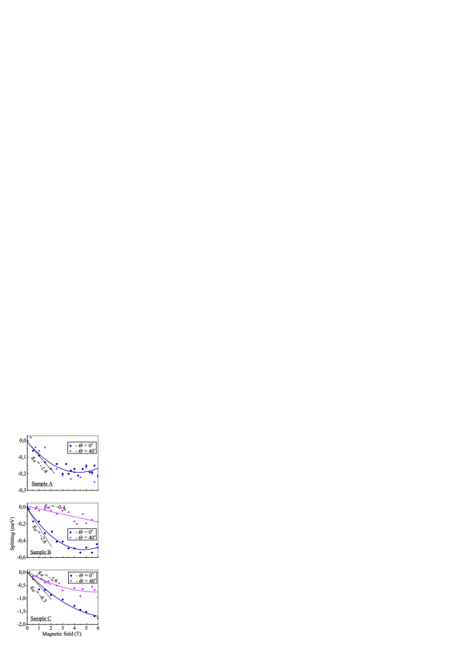
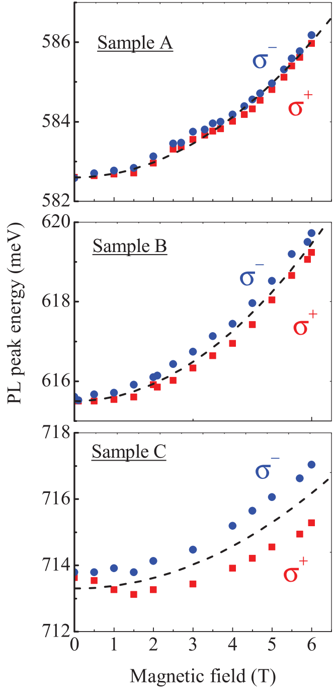
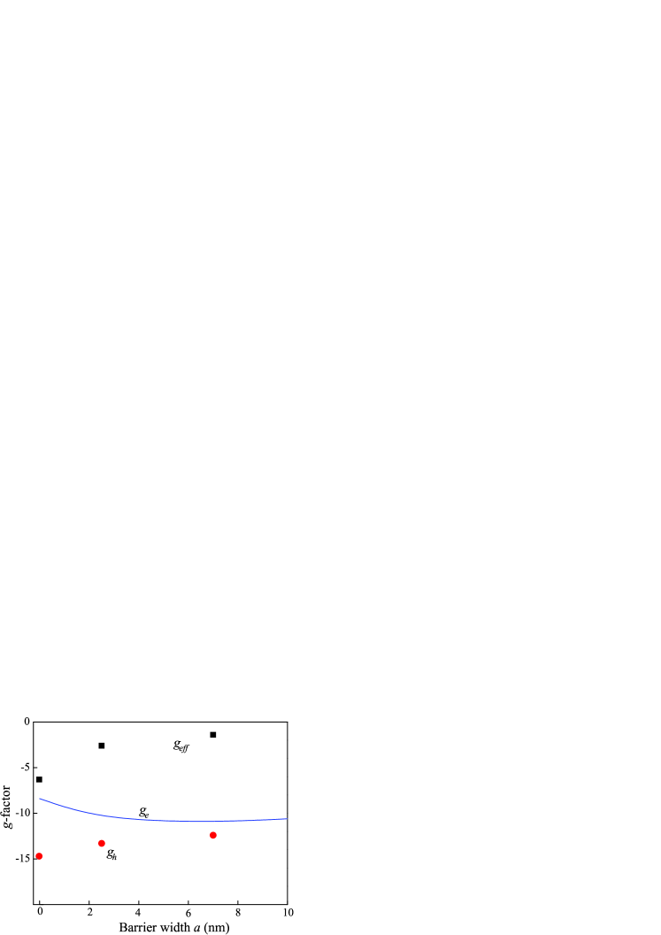
Detected splitting of PL lines in two circular polarizations reflects spin splitting of conduction and valence bands. The linear region of the Zeeman splitting (see Fig. 2) gives the value of the effective electron-hole -factor (), which is equal to the difference of -factors of the carriers that take part in the optical recombination, Terent'ev2014 . The extracted values of as a function of an InGaAs barrier width are presented in Fig. 4 and Tab. 1. It is clearly seen that the absolute value of tends to increase with decreasing width of InGaAs barrier.
While observed nonlinear character of Zeeman splitting in magnetic field is out of scope of present paper, it is worth mentioning that highly nonlinear Zeeman splitting of excitons was also detected in AlGaAs/GaAs and InGaAs/GaAs systems and the model was suggested that is based on a spin-dependent field-induced admixture between the light- and heavy-hole valence bands Traynor1997 .
Large FWHM of the PL peak and its decay detected in sample C is explained in terms of effective scattering by charged centers at QW interfaces. In this structure QW interfaces are formed by InAs and InAlAs layers having large lattice mismatch and therefore are characterized by large defects density. Apparently scattering on these defects is responsible for the strong decay of optical recombination efficiency, increase of FWHM as well as depolarization of the emission in the case of the magnetic field applied.
| Sample A | Sample B | Sample C | |
| -1.4 | -2.6 | -6.3 | |
| -11 | -10.7 | -8.4 | |
| -12.4 | -13.3 | -14.7 | |
| – | -9 | -13.2 | |
| – | -9.4 | -15.8 | |
| (meV/T2) | 0.095 | 0.11 | 0.08 |
Now we turn to separate determination of electron and hole -factors. It was found that the -factor of hole is extremely sensitive to the separation between heavy-hole and light-hole quantization levels, which in turn depends on the unknown strength of strain fields and localization potential. Hence we only calculate , which is less affected by the localization potential and strain, and therefore can be evaluated with much higher accuracy. Then we estimate the value of using experimentally determined and
| (1) |
Computation method is based on numeric diagonalization of the 14-band Hamiltonian in the presence of magnetic field DurnevPRB2014 ; Durnev2014 . We use the developed in Ref. DurnevPRB2014 14-band -model for calculation of electron and hole states at zero magnetic field, and use obtained wave functions to calculate the Zeeman splitting at small magnetic fields in the framework of perturbation theory (the approach is analogous to the one used to calculate heavy-hole and light-hole -factors in the framework of Luttinger Hamiltonian, see Eqs. (9a), (9b) of Ref. [Durnev2014, ]). The band parameters of InAs and its alloys were taken from Refs. Meyer2001 ; Walle1989 , and confining potentials for electron and holes were calculated using the model of Ref. Walle1989 taking into account elastic strain present in the structure. The interband matrix elements of momentum operator were taken from Ref. Jancu2005 .
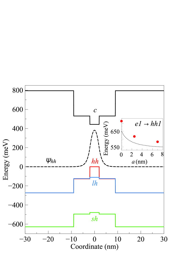
The evaluated band diagram, wave function of heavy hole at zero in-plane momentum , and optical transitions energies are presented in Fig. 5. Theoretical model gives close-to-experiment values of optical transitions energies and the in-plane electron mass ( as determined from transport measurements in similar structures Richter2000 ; Moller2003 ; Hu2003 ). It also provides a good agreement between theoretical and experimentally measured values of Danilov2015 ; Moller2003 ; Hu2003 . The discrepancy between theoretically calculated and experimental values of optical transitions energies is possibly attributed to the presence of in-plane localization potentials, which lead to increase of the PL peak energy.
Evaluated values of hole Landé factors as well as theoretical values of and experimentally measured are presented in Fig. 4 and Tab. 1. As we mentioned above theoretical calculations do not allow to obtain with sufficient precision. Its values obtained in the framework of 14-band -model, used for evaluation of , lie in the range of for the studied structures Danilov2015 , and differ significantly from those given in Tab. 1.
In order to study anisotropy of hole -factor we have carried out experiments in a tilted magnetic field. While electron Zeeman splitting is known to be almost independent of the direction of applied magnetic field ivch_book , the spin splitting of a heavy hole bound to QW potential must be sensitive to a normal component of magnetic field only, because the in-plane heavy-hole -factor is close to zero in III-V quantum wells Marie01 . Hence tilted magnetic field should result in modification of . Indeed, heavy-hole -factor in a magnetic field tilted by an angle with respect to QW normal is
| (2) |
where and are the components of the -factor tensor for parallel to the growth axis and oriented in the plane of QW. Since is close to zero, and its absolute value must be reduced at .
For example, the 40∘ tilt of the field is expected to result in reduction of from -13.3 and -14.7 to -10.2 and -11.3 for samples B and C, respectively. In turn, assuming is independent of , the value of is predicted to change to 0.5 and -2.9 for these samples. Comparison with Fig. 2 shows that these estimated values are close to the values observed in experiment.
Anomalous behaviour of the Zeeman splitting was observed in structure A only. As seen from Fig. 2, the effective Zeeman splitting is almost unaffected by the tilt of in this sample. It may indicate, that the heavy hole in this sample is localized by rather a three dimensional potential than the potential of QW. This suggestion is consistent with the value of the in-plane localization length of hole nm (see below for details), which in the case of sample A is less than the effective localization in the -direction (see Fig. 5). The possible source for such a three-dimensional confinement is a Coulomb potential of charged centers in quantum well layers.
With the use of Eqs. (1) and (2) it is possible to evaluate and independently without theoretical calculations by measuring at two different angles :
| (3) | |||||
The calculated values are presented in Tab 1.
Let us finally analyze the diamagnetic shift of PL lines, see Fig. 3. The value of diamagnetic shift is given by a half-sum of the and -polarized components and is well fitted by the quadratic function . The extracted values of are listed in Tab. 1. To derive theoretical expression for we will use a simple model of the carriers bound by a parabolic in-plane potential in the form Sugawara1997 ; PhysRevB.57.9088
| (4) |
where is the in-plane coordinate, is the effective in-plane mass, is the in-plane localization length of an electron () and heavy-hole (), and is the Planck constant. Making the Peirels substitution for the carrier wave vector in magnetic field and solving the Schrödinger equation with potential (4) we find for the diamagnetic coefficient
| (5) |
where is the electron charge, and is the speed of light. Since in QWs under study (electron mass Richter2000 ; Moller2003 ; Hu2003 , heavy-hole mass is deduced from the calculations for sample A) we conclude that the main contribution to the diamagnetic shift results from a confined electron. Taking experimentally measured values of we find that the in-plane localization length for an electron is nm in all studied samples. Localization length for a hole is nm and is even smaller than .
V Conclusions
To summarize, series of magneto-optical experiments have been carried out on narrow gap InAlAs/InGaAs/InAs QWs with different width of InGaAs barrier in both perpendicular and tilted magnetic fields. Effective electron-hole -factor is measured directly from the splitting of magneto-PL line into circularly-polarized terms. The values of electron -factor are calculated theoretically while the -factor of holes is estimated by extracting from the total splitting. Experiments in tilted magnetic field were used to investigate anisotropy of the heavy hole -factor.
Acknowledgements.
The authors are grateful to S. A. Tarasenko for interest in the work and useful discussions. The authors gratefully acknowledge financial support from DFG SFB 689, Ya.V.T. and S.V.I. are thankful to the support from RSF (Project 15-12-30022). M.V.D. acknowledges financial support from RFBR project No. 16-32-60175 and the Dynasty foundation.References
- (1) K. Inoue, J.C. Harmand and T. Matsuno, J. of Cryst. Growth 111, 313 (1991).
- (2) E. Tournié, O. Brandt, and K. Ploog, Appl. Phys. Lett. 60, 2877 (1992).
- (3) Ya. V. Terent’ev, S.N. Danilov, J. Loher, D. Schuh, D. Bougeard, D. Weiss, M.V. Durnev, S.A. Tarasenko, M.S. Mukhin, S.V. Ivanov, and S.D. Ganichev, Appl. Phys. Lett. 104, 101111 (2014).
- (4) A. Richter, M. Koch, T. Matsuyama, Ch. Heyn, and U. Merkt, Appl. Phys. Lett. 77, 3227 (2000).
- (5) Ch. Heyn, S. Mendach, S. Löhr, S. Beyer, S. Schnüll, and W. Hansen, J. Crist. Growth 251, 832 (2003).
- (6) C.H. Möller, Ch. Heyn, and D. Grundler, Appl. Phys. Lett. 83, 2181 (2003).
- (7) M. Hirmer, D. Schuh, and W. Wegscheider, Appl. Phys. Lett. 98, 082103 (2011).
- (8) K. Tsumura, S. Nomura, T. Akazaki, and J. Nitta, Phys. E 34, 315 (2006).
- (9) Ya.V. Terent’ev, S.N. Danilov, H. Plank, J. Loher, D. Schuh, D. Bougeard, D. Weiss, M.V. Durnev, S.A. Tarasenko, I.V. Rozhansky, S.V. Ivanov, D.R. Yakovlev and S.D. Ganichev, J. Appl. Phys. 34, 113906 (2015).
- (10) C.-M. Hu, C. Zehnder, Ch. Heyn, and D. Heitmann, Phys. Rev. B 67, 201302(R) (2003).
- (11) J. Nitta, Y. Lin, T. Akazaki, and T. Koga, Appl. Phys. Lett. 83, 4565 (2003).
- (12) U. Wurstbauer, M. Soda, R. Jakiela, D. Schuh, D. Weiss, J. Zweck, W. Wegscheider, J. of Cryst. Growth 311, 2160 (2009).
- (13) U. Wurstbauer, S. Sliwa, D. Weiss, T. Dietle, and W. Wegscheider, Nature Physics 6, 955 (2010).
- (14) S.D. Ganichev, S.A. Tarasenko, V.V. Bel’kov, P. Olbrich, W. Eder, D.R. Yakovlev, V. Kolkovsky, W. Zaleszczyk, G. Karczewski, T. Wojtowicz, and D. Weiss, Phys. Rev. Lett. 102, 156602 (2009).
- (15) P. Olbrich, C. Zoth, P. Lutz, C. Drexler, V.V. Bel’kov, Ya. V. Terent’ev, S.A. Tarasenko, A.N. Semenov, S.V. Ivanov, D.R. Yakovlev, T. Wojtowicz, U. Wurstbauer, D. Schuh, and S.D. Ganichev, Phys. Rev. B 85, 085310 (2012).
- (16) F. Capotondi, G. Biasiol, D. Ercolani, V. Grillo, E. Carlino, F. Romanato, and L. Sorba, Thin Solid Films 484, 400 (2005).
- (17) V.V. Bel’kov and S.D. Ganichev, Semicond. Sci. and Tech. 23, 114003 (2008).
- (18) Chongyun Jiang, V.A. Shalygin, V.Yu. Panevin et al, Phys. Rev. B 84, 125429 (2011).
- (19) P.D. Wang, N.N. Ledentsov, C.M. Sotomayor Torres, I.N. Yassievich, A. Pakhomov, A.Yu. Egovov, P.S. Kop’ev, and V.M. Ustinov, Phys. Rev. B 50, 1604 (1994).
- (20) Mitsuru Sugawara, Yoshiaki Nakata, Kohki Mukai, and Hajime Shoji, Phys. Rev. B 55, 13155 (1997).
- (21) S. N. Walck and T. L. Reinecke, Phys. Rev. B 57, 9088 (1998).
- (22) N.J. Traynor, R.J. Warburton, M.J. Snelling, R.T. Harley, Phys. Rev. B 55, 15701 (1997).
- (23) M. V. Durnev, M. M. Glazov, and E. L. Ivchenko, Phys. Rev. B 89, 075430 (2014).
- (24) M.V. Durnev, Phys. Solid State 56, 1416 (2014).
- (25) I. Vurgaftman, J.R. Meyer, and L.R. Ram-Mohan, Jour. of Appl. Phys. 89, 5815 (2001).
- (26) C.G. Van de Walle, Phys. Rev. B 39, 1871 (1989).
- (27) J.-M. Jancu, R. Scholz, E. A. de Andrada e Silva, and G. C. L. Rocca, Phys. Rev. B 72, 193201 (2005).
- (28) S.N. Danilov, Ya.V. Terent’ev, J. Loher, D. Bougeard, D. Weiss, M.V. Durnev, S.V. Ivanov and S.D. Ganichev, 23rd Int. Symp. Nanostructures: Physics and Technology, Saint Petersburg, Russia, June 22-26, 2015. (NC.02o)
- (29) A. V. Malyshev, I. A. Merkulov, and A. V. Rodina, Phys. Stat. Solidi B 210, 865 (1998).
- (30) B. L. Gelmont and M. I. Dyakonov, Fiz. Tekh. Poluprov. 7, 2013 (1973) [Soviet Phys. Semicond. 7, 1345 (1974)].
- (31) E. L. Ivchenko, Optical spectroscopy of semiconductor nanostructures (Alpha Science Internat., Harrow, UK, 2005).
- (32) X. Marie, T. Amand, P. Le Jeune, M. Paillard, P. Renucci, L. E. Golub, V. D. Dymnikov, and E. L. Ivchenko, Phys. Rev. B 60, 5811 (1999).