Quantum Transport Characteristics of Lateral pn-Junction of Single Layer TiS3
Abstract
Using density functional theory and nonequilibrium Green’s functions-based methods we investigated the electronic and transport properties of monolayer TiS3 pn-junction. We constructed a lateral pn-junction in monolayer TiS3 by using Li and F adatoms. An applied bias voltage caused significant variability in the electronic and transport properties of the TiS3 pn-junction. In addition, spin dependent current-voltage characteristics of the constructed TiS3 pn-junction were analyzed. Important device characteristics were found such as negative differential resistance and rectifying diode behaviors for spin-polarized currents in the TiS3 pn-junction. These prominent conduction properties of TiS3 pn-junction offer remarkable opportunities for the design of nanoelectronic devices based on a recently synthesized single-layered material.
I Introduction
In recent years, two-dimensional materials have attracted a lot of interest due to their wealth of potential applications in various fields. Among the large family of two-dimensional materials, transition metal dichalcogenides (TMDs) stick out due to their exceptional electronic and optical properties.Novoselov ; Wang ; Chhowalla TMDs are van der Waals (vdW) stacked layered materials.Zhao ; Geim ; Cunningham Many of the TMDs have been shown to undergo an indirect-to-direct band gap transition when exfoliated down to a monolayer.Mak ; Zhao1 Thus they are direct band gap semiconductor in the monolayer form. Due to the chemical versatility of this class of materials they exhibit a wide range of mechanical, electronic and optical characteristics.Jariwala ; Splendiani ; Manzeli ; Elder
In addition to TMDs there is important class of materials that are stable in atomic layer form: transition metal trichalcogenides (TMTs). Similar to TMDs, TMTs also exhibit layered structures that are held together by weak vdW interactions. Most of the crystal structures of TMTs belong to the space group P21/m and they consist of one-dimensional chains of trigonal prisms with the metal atom occupying the center of each prism. Unlike the TMDs, single, few layer or even macroscopicly thick TMTs may display direct-gap semiconducting behavior. Electronic and optical properties of various types of bulk TMTs such as ZrSe3, HfSe3, TiS3, ZrS3, ZrTe3 have been investigated experimentally.Hoesch ; Pacile ; Gorlova1 ; Guilmeau Previous studies have shown that, bulk TiS3 is an n-type semiconductor with an energy band gap of 1 eV and it was shown that, it has a room temperature electronic mobility of about 30 cm2 V-1s-1.Finkman A nonlinear current-voltage characteristics of bulk TiS3 has been observed below 60 K.Gorlova2 Compared to TMDs, TMTs have drawn little attention until recently, which changed when the single layer TiS3 was isolated.Island
The exfoliation of a single layer of titanium trisulfide (TiS3), has triggered tremendous interest in the electronic device community.Island Recently Jin et al. theoretically studied structural, electronic and optical properties of titanium and zirconium trichalcogenide monolayers and they found that monolayers of TiTe3 and ZrTe3 are metallic, TiSe3, ZrSe3, and ZrS3 are indirect while TiS3 is a direct band gap semiconductor.Jin Moreover, they showed that these monolayer semiconductors exhibit anisotropic conductive properties. The effect of tensile strain on the electronic properties of monolayers of TMTs have been studied.Li We have recently investigated structural and electronic properties of defective and oxidized monolayer TiS3.Iyikanat Previous experimental studies on monolayer TiS3 have revealed that it has a direct band gap of 1.10 eV and it exhibits a high carrier mobility in the few-layer limit.Ferrer ; Ferrer1 . Recently, novel field-effect transistors based on few-layer TiS3 were demonstrated.Lipatov ; Island . Island et al. showed that, these transistors demonstrate promising device characteristics such as electron mobility of 2.6 cm2 V-1s-1 and n-type semiconducting behavior with ultrahigh photoresponse and fast switching times at room temperature.Island Strain engineering has been identified as one of the most promising strategies to tune the band gap because the reduced-dimensional structures can sustain much larger strains than bulk crystals.Kang1 ; Kang Strong nonlinearity of the current-voltage characteristics has been reported by Gorlova et al. Gorlova ; Gorlova3 Especially, the nonlinearity in the current-voltage characteristics, the relatively high carrier mobility and the direct band gap properties even for a thickness of hundreds of layers make TiS3 a potential candidate for future electronics.
In the present study, structural, electronic, magnetic and transport properties of p- and n-doped TiS3 are investigated. The computational methodology is given in Sec. 2. Structural, electronic and magnetic properties of pristine, Li, and F doped monolayers of TiS3 are studied in Sec. 3 and 4. Transport properties of TiS3 pn-junction are investigated in Sec. 5. We summarize our results in Sec. 6.
II Computational Methodology
All ionic and electronic relaxations are carried out within the framework of spin-polarized density functional theory (DFT) method implemented in the SIESTA package.Siesta The Perdew-Burke-Ernzerhof generalized gradient approximation (PBE-GGA) is used for the exchange correlation functional. The Grimme’s DFT-D2 dispersion correction is used to include the long-range vdW interactions. PBE ; Grimme A double- polarized basis set is used and the mesh cutoff is chosen as 350 Ry. The convergence criterion for the energy is taken as 10-5 eV. All atomic positions are fully relaxed with a force tolerance of 0.04 eV/Å. A vacuum space of at least 15 Å is used to prevent undesirable interactions between adjacent layers. Pressures on the unitcell are decreased to values less than 1.0 kBar. Structural calculations are performed with a Monkhorst-Pack Grid. A k-point sampling of is used for geometric calculations in supercell. The Bader charge population analysis is performed to calculate the charge transfer between adatoms and TiS3.Henkelman
The electronic transport calculations are performed by using the TRANSIESTA code, which is based on nonequilibrium Green’s function formalism and DFT (NEGF-DFT).Transiesta The current through the central region is evaluated by the Landauer-Büttiker formula
| (1) |
where E denotes the energy, and are the electrochemical potentials of the left and right electrodes, V is the applied voltage, T(E, V) is the quantum mechanical transmission probablity of electrons. e, h and f denote electron charge, Planck’s constant and Fermi function, respectively. Fully relaxed coordinates for the transport calculation, with a mesh cutoff of 350 Ry and a double- polarized basis set are used. The Brillouin zone normal to the transport direction is sampled by a k-point mesh of .
III Structural and Electronic Properties of Single Layer TiS3
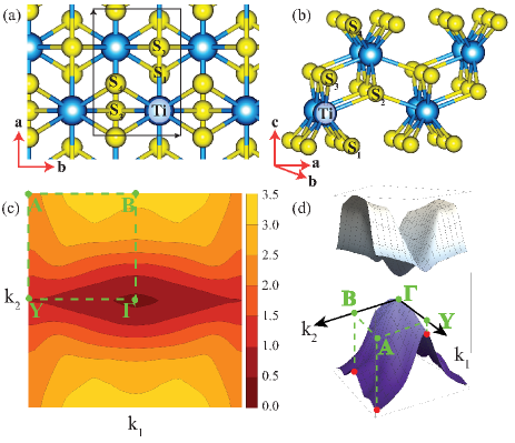
The calculated lattice constants of monolayer TiS3 are a Å and b Å, which are compatible with the previous studies. Kang ; Jin As seen in Fig. 1(a), atoms in TiS3 are arranged in a chain-like structure which consists of a prismatic trigonal structure with the metal atom located at the centre and chalchogen atoms located at the corners of the prism. The unit cell of TiS3 consists of two Ti atoms and six S atoms, which is shown in Fig. 1(a). To demonstrate more clearly the geometric structure of TiS3, S atoms from different planes of TiS3 are illustrated with different labels. Fig. 1(b) presents a side view of TiS3. As shown in this figure, S atoms located on the bottom plane of TiS3 are labeled as S1, whereas S atoms placed on the top plane of TiS3 are labeled as S4. These surface S atoms are bonded strongly to the Ti atoms with a bond lenght of 2.50 Å. Correspondingly, S atoms located in the middle of the TiS3 layer are denoted as S2 and S3. The locations of S2 and S3 atoms in the structure are geometrically equivalent, and the bond lenghts of the S2 and S3 atoms to the first and second nearest neighbour Ti atoms are 2.48 Å and 2.65 Å, respectively.
To investigate the electronic structure we performed a Bader analysis of the charge density as obtained from the SIESTA code. In a Bader charge analysis, atoms are defined by volumes bounded by surfaces of zero-flux. In these surfaces the gradient of the charge density is perpendicular to the normal vector of the surface. The integrated charges in the volume attributed to atoms are defined as Bader charge. In TiS3, the bonds between inner-plane S atom (S2 or S3) and a Ti atom show ionic character with a charge transfer of 1.0 e depleted from Ti atom to S atom. On the other hand, Ti atom donates 0.9 e of valence charges to the two surface atoms (two S1 or two S4 atoms). These two surface S atoms share 0.9 e and make a covalent bond with the Ti atom. As a result, in monolayer TiS3, Ti atom has 2.1 e, S2 and S3 atoms possess 7.0 e and S1 and S4 atoms have 6.45 e.
Nanosheets and nanoribbons of TiS3 are used to fabricate FETs. While fabricated nanosheets exhibit high mobilities, nanoribbons exhibit higher optical response and gate tunability, but have lower mobility. Island Previous experimental and theoretical studies have shown that, exceptional chain-like structure of TiS3 leads to anisotropic conductive properties, i. e. the resistivity of TiS3 across the chains are significantly higher than the resistivity along the chains. Gorlova1 ; Jin In order to properly understand the electronic properties of TiS3, contours plots of band gap energies in reciprocal space of TiS3 are depicted in Fig. 1(c). Monolayer TiS3 is a direct-gap semiconductor with a band gap of 1.10 eV.Iyikanat ; Li ; Jin . Our PBE calculated band gap value of TiS3 is 0.45 eV. It is well known that the bare PBE underestimates the band gap values of semiconductors. However, the electronic band dispersion is well-approximated by PBE. As seen from Fig. 1(c), TiS3 has a direct band gap with both the valence-band-maximum (VBM) and the conduction-band-minimum (CBM) residing at the point, and variation of the gap along the -Y direction is small. VB and CB give quite valuable information about the electronic structure of a material. Three-dimensional surface plots of VB and CB of TiS3 are shown in Fig. 1(d). The plotted surfaces clearly show that VB and CB surfaces are highly anisotropic. The electron mobility along k2 direction is much larger than that along the perpendicular direction. This makes it clear that the contribution to the electronic conductivity parallel to the chain direction will be much larger than that corresponding to normal to the chain direction.
IV p- and n- Type Doping of TiS3
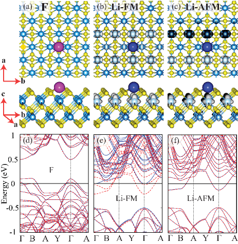
Top and side views of the relaxed geometric structure of F-doped TiS3 are shown in Fig. 2(a). Li-doped TiS3 has magnetically two different states which are denoted as Li-FM and Li-AFM and shown in Figs. 2(b) and (c), respectively. The structural and electronic properties of these states are given in Table 1. As shown in Figs. 2(a)-(c), both adatoms are placed in the middle of the four S atoms. While Li atom binds at a distance 0.86 Å, F atom is located 0.79 Å above the surface. In order to hinder the interactions between the adatoms of adjacent supercells, a supercell is used for electronic structure calculations. Both Li and F atoms do not cause any significant structural deformation, thus TiS3 preserves its lattice constant values, which are in the supercell form and Å. The binding energies are calculated using the expression , where Ebind is the binding energy of the considered adatom, E is the energy of adatom doped TiS3, E is the energy of pristine TiS3 and EAdatom is the energy of the considered adatom. As listed in Table 1, binding energies of F, Li-FM, and Li-AFM on TiS3 are calculated to be 2.48 and 2.98, and 2.99 eV, respectively.
| Binding | Ebind | ||||
|---|---|---|---|---|---|
| (Å) | Site | (eV) | (e) | () | |
| F | 0.79 | H | 2.48 | -0.6 | 0.0 |
| Li-FM | 0.86 | H | 2.98 | +1.0 | 0.9 |
| Li-AFM | 0.86 | H | 2.99 | +1.0 | 0.0 |
Bader charge analysis shows that F adatom gains 0.6 e when it is placed on TiS3. Contrary to F, Li adatom donates all its valence charge (1 e) to TiS3. The non-magnetic nature of the monolayer TiS3 is not affected by F doping. However, Li doping significantly changes the magnetic properties of TiS3 and two different magnetic states are generated. One of them is denoted as Li-FM state, and the other is denoted as Li-AFM state and as given in Table 1 their magnetic moment values are 0.9 and 0.0 per supercells. Our results show that Li-FM is the ground state. However, calculated energy difference between Li-FM and Li-AFM states is only 5 meV. Thus, Li-AFM state can not be ignored and both of the states are considered in the present paper. Spin polarized charge densities of Li-doped TiS3 for FM and AFM states are shown from top and side views in Figs. 2(b) and (c), respectively. As seen in the figure of Li-FM, Ti atoms of the nearest two chains to the Li adatom are polarized ferromagnetically. While the nearest Ti atom to the Li adatom has a magnetic moment of 0.21 , this value decreases to 0.14 for the furthest Ti atom. On the other hand, Fig 2(c) shows that Ti atoms of the nearest two chains to the Li adatom are polarized antiferromagnetically. As in the case of Li-FM, magnetic moments of individual Ti atoms are decreasing when the distance to the Li adatom is increased. Absolute values of magnetic moment of individual Ti atoms are almost the same in the Li-FM and Li-AFM states. However, in both cases S atoms do not exhibit any significant magnetic moment.
In order to investigate the effect of adatom doping on the electronic structure of TiS3, band diagrams of F- and Li-doped TiS3 are calculated and showed in Figs. 2(d)-(f). As mentioned above Li-doped TiS3 has two different magnetic states with very similar energy values and their band diagrams are also shown in these figures. Fig. 2(d) shows that, when TiS3 is doped with F atoms, some states of TiS3 discharge because F atom recieve 0.6 e- from it. Thus, F doping results in acceptor states close to the top of the valence band. These results suggest that F doping causes p-type doping of TiS3. Flat bands of F atoms appear 0.3 eV below the Fermi level. On the other hand, donor states occur close to the conduction band minimum when TiS3 is doped with Li atoms. Fig. 2(e) shows that, the donor states come from only the majority spin component in the Li-FM state. However, as shown in Fig. 2(f), in the Li-AFM state all bands are degenerate and the donor states originate from charges with both spin components. Adsorption of Li atoms on TiS3 leads to n-type doping. Created donor and acceptor states are necessary for the construction of a pn-junction. Thus, doping one side of a TiS3 layer with F (a p-type dopant) and the other side with Li (an n-type dopant) forms a pn-junction. One can modulate the electronic properties of TiS3 by changing the atom type of the dopant and the doping concentrations.
V Transport properties of TiS3 PN-JUnction
A pn-junction can be constructed by combining p-type and n-type materials in lateral or vertical orientation. Because of the controllability of its electronic properties and its possible applications, pn-junctions are used in many semiconductor devices. To construct a pn-junction, the presence of shallow p- and n-type doping levels are essential. In the previous part, we have shown that, p- and n-type doping of TiS3 can be realized through doping with F and Li atoms, respectively. Thus when we construct a device which consist of p-type and n-type doped parts of TiS3, states near the valence and conduction bands will behave like acceptor and donor states. The quantum transport properties of a monolayer TiS3-based pn-junction are investigated in the following.
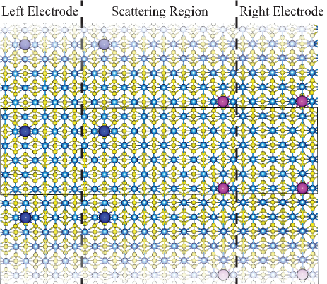
The device setup used for the transport calculations on the TiS3 pn-junction is shown in Fig. 3. The device geometry consists of semi-infinite left electrode, semi-infinite right electrode, and a scattering region. The possibility of experimental realization of TiS3 pn-junction is higly dependent on the dopant atom concentrations. Thus, to simulate the electrode parts of the device, one adatom of Li or F and a supercell of TiS3 are used. In the present study, ground state of Li-FM is used for the transport calculations of TiS3 pn-junction. The adatom concentration is the same 51013 cm-2 for both electrodes. The distance between Li and F atoms in the scattering region is taken to be 22.7 Å. Recent studies have shown that, monolayer TiS3 exhibits conductance anisotropy, and the electron mobility along the chain direction is larger than across the chain direction.Gorlova1 ; Jin Therefore, the transport direction of the device geometry is choosen to be the chain direction.
Fig. 4 presents transmission profiles per unit lenght of constructed TiS3 pn-junction for varying bias voltages. As shown in Fig. 4(c), in the unbiased situation TiS3 pn-junction has a transport gap of 0.99 eV. VBM and CBM of this transmission gap coincides with the VBM of Li doped TiS3 and CBM of F doped TiS3, respectively. Inset of Fig. 4(c) shows transmission profile of TiS3 pn-junction zoomed around the Fermi level, which is shown by dashed rectangle. These small transmissions occur when the valence band states of F doped region overlap with the conduction band states of Li doped region. Therefore, charges from valence band of the F doped source region can tunnel to the empty conduction band of Li doped region. As shown in Figs. 4 (a)-(f), applying bias voltage leads to significant modulation in the electronic properties of TiS3 pn-junction.
First of all, increasing bias voltage of pn-junction shifts the energy bands of F doped electrode to the lower energy values, whereas it shifts the energy bands of Li doped electrode to higher energy values. As a result, when the bias voltage is increased from -0.2 V to 0.3 V, the transport gap of the TiS3 pn-junction decreases from 1.19 eV to 0.68 eV.
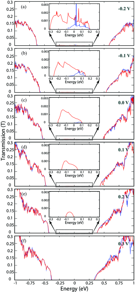
Secondly, while transmission values near to the VBM and CBM look similar, for high energy values such as -1.0 eV, transmission values are increasing from 0.15 to 0.30 with increasing bias voltage from -0.2 V to 0.3 V. As can be seen from Fig. 2, near to the edges of the CBM of F doped TiS3 and the VBM of Li doped TiS3 consist of a smaller number of bands relative to the deeper energies. When bias voltage is increased, deeper states of p-type doped and n-type doped parts of the TiS3 contribute to the transmission. Thus, rising of the transmission values of TiS3 pn-junction to high energy ranges can be expressed by the shifting of deeper states of the left and right electrodes. On the other hand, spin-up and spin-down transmission profiles are almost the same for the considered energy range and bias values.
Lastly, Fig. 4 shows that, transmission in the vicinity of the Fermi level is decreasing with increasing bias voltage from -0.2 to 0.3 V. Due to quantum tunnelling between the electrodes, there is only small transmission between energy values of -0.2 and 0.1 eV, even in the unbiased situation, which is shown in the inset of Fig. 4(c). In the previous part, we showed that Li doped TiS3 is magnetic. Ti atoms near to the adsorbed atom possess a net magnetic moment with the same spin polarization. Therefore, transmission values of TiS3 pn-junction near the Fermi level are highly spin-polarized. Figs. 4(d)-(f) show that, with increasing bias voltage, the transmission near the Fermi level decreases and at 0.3 V bias it is completely suppressed. On the other hand, when the bias voltage is increased in the other direction, energy range with the nonzero transmission and transmission values near the Fermi level increases for both spin components. Moreover, some small resonant states occur for applied bias voltage of -0.2 V, which is shown in the inset of Fig. 4(a).
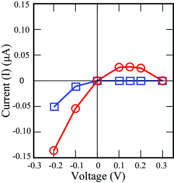
The spin-up and spin-down I-V characteristics of TiS3 pn-junction are shown in Fig. 5 by the red and blue curves, respectively. The corresponding current values are calculated for a scattering region of size 14.91 Å. Fig. 5 explicitly shows that, spin-up and spin-down I-V characteristics of TiS3 pn-junction are rather different. Also this figure clearly shows that spin-up current exhibits negative differential resistance (NDR), when positive bias applied to the system. Spin-up and spin-down current show typical diode behavior for negative bias. The NDR phenomenon in this system can be explained by the variation of transmissions and the relative shifts of energy states of device and electrode regions with applied bias voltage. As shown in Figs. 4(c)-(e), small spin-up transmission peaks near the Fermi level are visible for 0.0 V 0.3, and these transmission peaks disappear for bias voltage 0.3 V, whereas spin-down transmissions are zero for these positive bias voltage values. These small spin-up transmission peaks lead to negative differential resistance (NDR) between 0.0 V and 0.3 V in the spin-up I-V characteristic of TiS3 pn-junction, as shown in Fig. 5. However, the spin-down current is zero for the positive bias voltage. On the other hand, when negative bias voltage is applied, spin-up and spin-down transmission peaks occur near the Fermi level, with the dominant one being spin-up, as shown in Figs. 4(a), (b). As a result, the spin-up electrons flow more easily from the valence band of the F-doped electrode to the conduction band of the Li-doped electrode, than the spin-down electrons. This explains the higher spin-up current values of the TiS3 pn-junction for negative bias. Moreover, spin-up and spin-down transmission peaks near the Fermi level rise with increasing negative bias voltage. This leads to an increase in the spin-up and spin-down current values for higher negative bias voltages. As a result, the I-V characteristic of a TiS3 pn-junction is strongly related to the doping types, its effect on the magnetism and the amount of doping of the electrodes and scattering parts. While one spin component of the current shows NDR, both spin components of the current show a typical diode character.
VI Conclusions
In summary, we investigated electronic and transport properties of monolayer TiS3 pn-junction by using density functional theory and nonequilibrium Green’s functions method. Doping one side of a TiS3 layer with F adatom (a p-type dopant) and the other side with Li adatom (an n-type dopant) forms a lateral pn-junction. We showed that the conduction properties of TiS3 pn-junction can be tuned by applying a bias voltage. The predicted device showed NDR behavior only for one spin component of the current. Both spin components of the current had asymmetric characteristics with respect to the bias voltage, thus, they showed rectifying diode behavior. Prediction of a pn-junction based on monolayer TiS3 reveals a functional application of this new material.
VII acknowledgments
This work was supported by the bilateral project between TUBITAK (through Grant No. 113T050) and the Flemish Science Foundation (FWO-Vl). The calculations were performed at TUBITAK ULAKBIM, High Performance and Grid Computing Center (TR-Grid e-Infrastructure). FI, HS, and RTS acknowledge the support from TUBITAK Project No 114F397. H.S. acknowledges support from Bilim Akademisi-The Science Academy, Turkey under the BAGEP program.
References
- (1) K. S. Novoselov, D. Jiang, F. Schedin, T. J. Booth, V. V. Khotkevich, S. V. Morozov, and A. K. Geim, Proc. Natl. Acad. Sci. USA 2005, 102, 10451-10453.
- (2) Q. H. Wang, K. K.- Zadeh, A. Kis, J. N. Coleman, and M. S. Strano, Nat. Nanotechnol. 2012, 7, 699-712.
- (3) M. Chhowalla, H. S. Shin, G. Eda, L. -J. Li, K. P. Loh, and H. Zhang, Nat. Chem. 2013, 5, 263-275.
- (4) Y. Zhao, X. Luo, H. Li, J. Zhang, P. T. Araujo, C. K. Gan, J. Wu, H. Zhang, S. Y. Quek, M. S. Dresselhaus, and Q. Xiong, Nano Lett. 2013, 13, 1007-1015.
- (5) A. K. Geim and I. V. Grigorieva, Nature 2013, 499, 419-425.
- (6) G. Cunningham, M. Lotya, C. S. Cucinotta, S. Sanvito, S. D. Bergin, R. Menzel, M. S. P. Shaffer, and J. N. Coleman, ACS Nano 2012, 6, 3468-3480.
- (7) K. F. Mak, C. Lee, J. Hone, J. Shan, and T. F. Heinz, Phys. Rev. Lett. 2010, 105, 136805.
- (8) W. Zhao, Z. Ghorannevis, L. Chu, M. Toh, C. Kloc, P. -H. Tan, and G. Eda, ACS Nano 2013, 7, 791-797.
- (9) D. Jariwala, V. K. Sangwan, L. J. Lauhon, T. J. Marks, and M. C. Hersam, ACS Nano 2014, 8, 1102-1120.
- (10) A. Splendiani, L. Sun, Y. Zhang, T. Li, J. Kim, C. -Y. Chim, G. Galli, and F. Wang, Nano Lett. 2010, 10, 1271-1275.
- (11) S. Manzeli, A. Allain, A. Ghadimi, and A. Kis, Nano Lett. 2015, 15, 5330-5335.
- (12) R. M. Elder, M. R. Neupane, and T. L. Chantawansri, App. Phys. Lett. 2015, 107, 073101.
- (13) M. Hoesch, X. Cui, K. Shimada, C. Battaglia, S. -i. Fujimori, and H. Berger, Phys. Rev. B 2009, 80, 075423.
- (14) D. Pacilé, M. Papagno, M. Lavagnini, H. Berger, L. Degiorgi, and M. Grioni, Phys. Rev. B 2007, 76, 155406.
- (15) I. G. Gorlova, V. Y. Pokrovskii, S. G. Zybtsev, A. N. Titov, and V. N. Timofeev, JETP 2010, 111, 298-303.
- (16) E. Guilmeau, D. Berthebaud, P. R. N. Misse, S. Hébert, O. I. Lebedev, D. Chateigner, C. Martin, and A. Maignan, Chem. Mater. 2014, 26, 5585-5591.
- (17) E. Finkman and B. Fisher, Solid State Commun. 1984, 50, 25-28.
- (18) I. G. Gorlova and V. Y. Pokrovskii, JETP Lett. 2009, 90, 295.
- (19) J. O. Island, M. Barawi, R. Biele, A. Almazán, J. M. Clamagirand, J. R. Ares, C. Sánchez, H. S. J. van der Zant, J. V. Álvarez, R. D’Agosta, I. J. Ferrer, and A. Castellanoz-Gomez, Adv. Mater. 2015, 27, 2595-2601.
- (20) M. Li, J. Dai, and X. C. Zeng, Nanoscale 2015, 7, 15385-15391.
- (21) F. Iyikanat, H. Sahin, R. T. Senger, and F. M. Peeters, J. Phys. Chem. C 2015, 119, 10709-10715.
- (22) Y. Jin, X. Li, and J. Yang, Phys. Chem. Chem. Phys. 2015, 17, 18665-18669.
- (23) I. J. Ferrer, J. R. Ares, J. M. Clamagirand, M. Barawi, and C. Sanchez, Thin Solid Films 2012, 535, 398-401.
- (24) I. J. Ferrer, M. D. Marciá, V. Carcelén, J. R. Ares, and C. Sanchez, Energy Procedia 2012, 22, 48-52.
- (25) A. Lipatov, P. M. Wilson, M. Shekhirev, J. D. Teeter, R. Netusil, and A. Sinitskii, Nanoscale 2015, 7, 12291-12296.
- (26) J. Kang, H. Sahin, H. D. Sengun, R. T. Senger, and F. M. Peeters, Phys. Rev. B 2015, 92, 075413.
- (27) J. Kang, H. Sahin, and F. M. Peeters, Phys. Chem. Chem. Phys. 2015, 17, 27742-27749.
- (28) I. Gorlova, S. Zybtsev, V. Y. Pokrovskii, N. Bolotina, I. Verin, A. Titov, Physica B 2012, 407, 1707-1710.
- (29) I. G. Gorlova, S. G. Zybtsev, and V. Y. Pokrovskii, JETP Letters 2014, 100, 256.
- (30) J. P. Perdew, K.Burke, and M. Ernzerhof, Phys. Rev. Lett. 1996, 77, 3865.
- (31) S. Grimme, J. Comp. Chem. 2006, 27, 1787-1799.
- (32) J. M. Soler, E. Artacho, J. D. Gale, A. García, J. Junquera, P. Ordejón, and D. Sánchez-Portal, J. Phys.: Condens. Matter 2002, 14, 2745-2779.
- (33) J. O. Island, M. Buscema, M. Barawi, J. M. Clamagirand, J. R. Ares, C. Sánchez, I. J. Ferrer, G. A. Steele, H. S. van der Zant and A. Castellanos-Gomez, Adv. Opt. Mater. 2014, 2, 641-645.
- (34) M. Barawi, E. Flores, I. J. Ferrer, J. R. Ares, C. Sánchez, J. Mater. Chem. A 2015, 3, 7959-7965.
- (35) G. Henkelman, A. Arnaldsson, and H. Jonsson, Comp. Mat. Sci. 2006, 36, 354-360.
- (36) M. Brandbyge, J.-L. Mozos, P. Ordejón, J. Taylor, and K. Stokbro, Phys. Rev. B 2002, 65, 165401.
- (37) L. Brattas and A. Kjekshus, Acta Chem. Scand. 1972, 26, 3441-3449.
- (38) S. Furuseth, L. Brattas, and A. Kjekshus, Acta Chem. Scand. A 1975, 29, 623-631.