Anisotropic Babinet-invertible metasurfaces to realize transmission–reflection switching for orthogonal polarizations of light
Abstract
The electromagnetic properties of an extremely thin metallic checkerboard drastically change from resonant reflection (transmission) to resonant transmission (reflection) when the local electrical conductivity at the interconnection points of the checkerboard is switched. To date, such critical transitions of metasurfaces have been applied only when they have 4-fold rotational symmetry, and their application to polarization control, which requires anisotropy, has been unexplored. To overcome this applicability limitation and open up new pathways for dynamic deep-subwavelength polarization control by utilizing critical transitions of checkerboard-like metasurfaces, we introduce a universal class of anisotropic Babinet-invertible metasurfaces enabling transmission–reflection switching for each orthogonally polarized wave. As an application of anisotropic Babinet-invertible metasurfaces, we experimentally realize a reconfigurable terahertz polarizer whose transmitting axis can be dynamically rotated by .
I Introduction
Metamaterials, which are artificial materials composed of engineered structures, exhibit exotic functionality not readily observed in nature Solymar and Shamonina (2009). Two-dimensional metamaterials with thicknesses much thinner than the wavelength of light, are called metasurfaces Kildishev et al. (2013). The careful design of metasurfaces enables us to control both the amplitude and phase of electromagnetic waves Monticone et al. (2013); Pfeiffer and Grbic (2013). Due to the scale invariance of Maxwell equations, the extraordinary properties of metamaterials and metasurfaces can be theoretically realized for all frequency ranges by altering the size of the structures. In the terahertz frequency range, metamaterials and metasurfaces are considered promising candidates for manipulating terahertz waves, because conventional electronics and photonics technologies cannot be directly applied. Various passive and active devices based on metamaterials and metasurfaces have been demonstrated in the terahertz frequency range Tao et al. (2011).
When designing metasurfaces in a vacuum, Babinet’s principle is often utilized. Babinet’s principle relates the scattering fields of a metasurface to a complementary metasurface. The complementary metasurface is obtained by applying a structural inversion to interchange the holes and metallic portions of the given one-layer metallic metasurface Booker (1946). For a more general case, consider a metasurface at with a spatially varying sheet impedance of , which relates the tangential component (namely, -component) of the electric field at on and the surface current density at the same point 111Rigorously, the sheet impedance is defined as , for the tangential component of the electric field on and surface current density on . Here, is an angular frequency and “c.c.” represents the complex conjugate operation.. The complementary surface with sheet impedance is obtained by applying a impedance inversion defined as , where is the impedance of the vacuum Baum and Singaraju (1974).
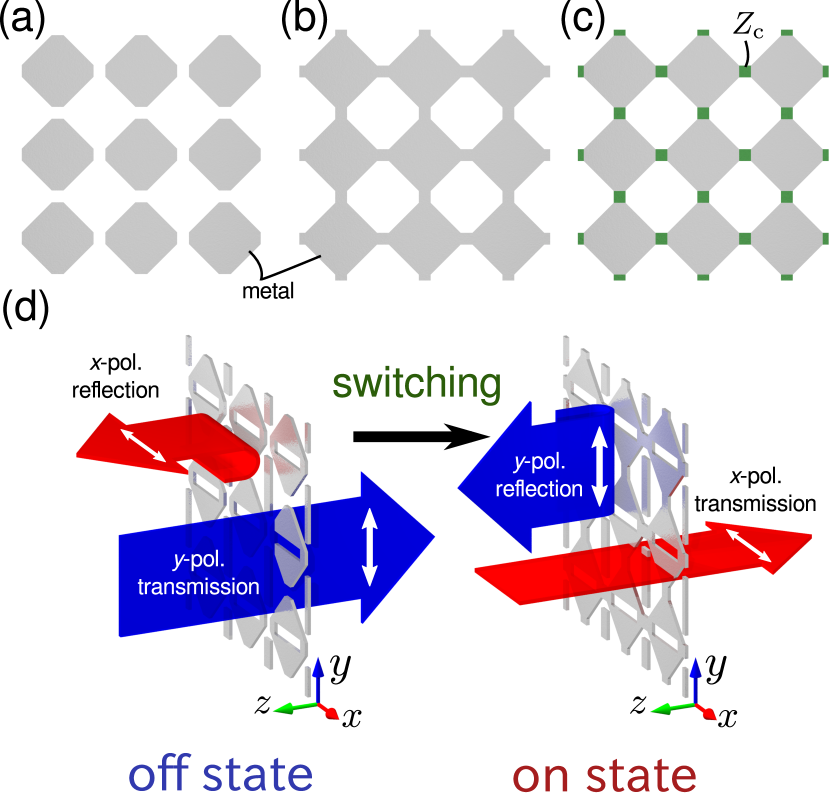
When considering Babinet’s principle, the metallic checkerboard is a special system: the disconnected [off-state; Fig. 1(a)] and connected [on-state; Fig. 1(b)] checkerboards are complementary with each other Compton et al. (1984). Their electromagnetic scattering properties drastically change when the connectivity of the checkerboard is altered. Such a critical behavior of checkerboard metasurfaces has been theoretically investigated from the perspective of percolation theory Kempa (2010) and experimentally observed in the microwave Edmunds et al. (2010) and terahertz frequency ranges Compton et al. (1984); Takano et al. (2014). The checkerboard metasurface has also been characterized in the optical region Ramakrishna et al. (2011). The critical property of checkerboard metasurfaces has been applied to reconfigurable transmission lines González-Ovejero et al. (2015a, b) and recently the critical behavior caused by rotational disorder has also been investigated Tremain et al. (2015).
To control the criticality of the checkerboard, resistive sheets with sheet impedance can be introduced at the interconnection points of the checkerboard, as shown in Fig. 1(c) Nakata et al. (2013); Urade et al. (2015, 2016a). The reconfigurable checkerboard is a checkerboard metasurface with dynamically controllable . If a metasurface is dynamically switchable to the metasurface congruent to the complement of the original, like the reconfigurable checkerboard, it is called Babinet invertible. Babinet-invertible metasurfaces are considered to be a generalization of the reconfigurable checkerboard. The 4-fold rotational symmetry of the reconfigurable checkerboard and Babinet’s principle lead to the relation
| (1) |
where the (zeroth-order) complex amplitude transmission coefficients of a normally incident plane wave with an angular frequency are denoted by and for the off-state () and on-state () metasurfaces, respectively 222Note that the complex amplitude transmission coefficient from an incident wave to a transmitted wave is defined by . In this paper, the modifier zeroth-order represents the case that satisfies , where is the projection operator onto (: transpose).. Then, the complementary switching of the reconfigurable checkerboard realizes transmission inversion, represented by Eq. (1). The transmission inversion of the reconfigurable checkerboard has been applied to a reconfigurable capacitive–inductive terahertz filter Urade et al. (2016b).
In previous studies of Babinet-invertible metasurfaces, 4-fold symmetry is assumed and the polarization dependence of the electromagnetic properties vanishes for normal incidence. Thus, the possibility of dynamic polarization control, which is essential for polarization-sensitive spectroscopy van der Valk et al. (2005); Katletz et al. (2012), through complementary switching has been unexplored. In this paper, the applicability limitation of the critical transition of checkerboard metasurfaces to dynamic deep-subwavelength polarization control is overcome by introducing a universal class of anisotropic Babinet-invertible metasurfaces enabling transmission inversions for each orthogonally polarized wave. To demonstrate one potential application of the proposed class of metasurfaces, we experimentally realize a reconfigurable terahertz polarizer as an anisotropic Babinet-invertible metasurface.
II Theory
If we break the rotational symmetry of Babinet-invertible metasurfaces, the (zeroth-order) complex amplitude transmission coefficients and for - and -polarized incident waves must be distinguished. Here, we consider an extension of Eq. (1) to such an anisotropic metasurface as follows:
| (2) | ||||
| (3) |
Equations (2) and (3) express transmission inversion separately for the two axes and . We therefore name this inversion transmission inversion for each orthogonal polarization, which requires a specific symmetry. Note that transmission inversion for each orthogonal polarization and the electric field continuation condition lead to transmission–reflection switching for each orthogonal polarization represented by
| (4) |
where is a complex amplitude reflection coefficient for an -polarized normally incident plane wave.
Next, we discuss the sufficient symmetry to realize transmission inversion for each orthogonal polarization. The rigorous vector version of Babinet’s principle is expressed as follows Nakata et al. (2013):
| (5) | ||||
| (6) |
where represents the (zeroth-order) complex amplitude transmission coefficient for a normally incident plane wave with -polarization onto the metasurface complementary to the off-state one () . Note that the polarization is rotated by 90∘ in the complementary problem compared with the original. Comparing Eqs. (5)–(6) with Eqs. (2)–(3), transmission inversion for each orthogonal polarization requires and . These equations are satisfied when the metasurface complementary to the off-state surface is obtained by 90∘ rotation of the on-state surface. This is the sufficient symmetry condition to realize transmission inversion for each orthogonal polarization.
As an application of transmission inversion for each orthogonal polarization, we consider the design of a polarizer whose transmitting axis can be dynamically rotated by , as shown in Fig. 1(d). Designing such a reconfigurable polarizer with variable-resistance elements requires simultaneous fine tuning for both the on- and off-state metasurfaces. This is difficult because the on- and off-state metasurfaces generally depend on each other. However, by utilizing transmission inversion for each orthogonal polarization, the problem can be drastically simplified. If we have an off-state Babinet-invertible metasurface with and at an angular frequency , then and are automatically satisfied for the on-state metasurface under transmission inversion for each orthogonal polarization. Then, the transmitting axis of the polarizer can be dynamically rotated by 90∘. The problem is reduced to designing the off-state Babinet-invertible metasurface with and .
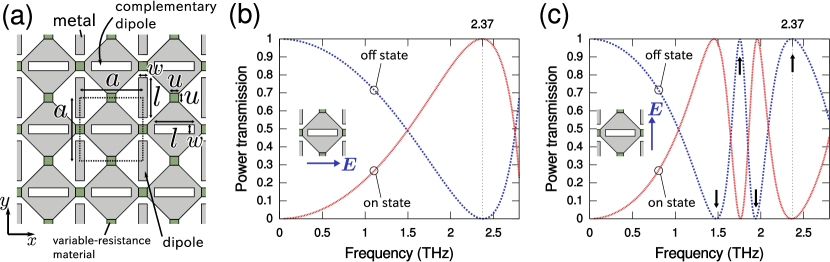
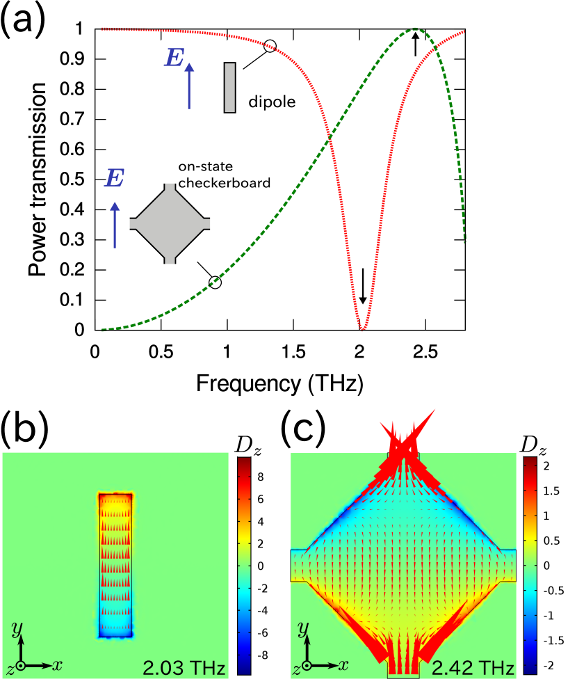
We design the reconfigurable terahertz polarizer by using the finite element method solver (COMSOL Multiphysics). To break the 4-fold symmetry of the checkerboard, we nest dipoles with their complementary pairs into the checkerboard so that the sufficient condition to realize transmission inversion for each orthogonal polarization can be satisfied. The design of a dipole-nested Babinet-invertible checkerboard metasurface (D-checkerboard) on is shown in Fig. 2(a). To simplify the analysis, we assume that all the metal sections are zero-thickness perfect electric conductors. The calculations are performed in the unit cell and periodic boundary conditions are applied to the sides. The top and bottom boundaries are set as ports with only fundamental modes. The plane wave generated by the top port normally enters a metasurface from to . The basic parameters are set as and . The dipoles and their complements respond only for polarization. For -polarized normally incident waves, the structure responds like a checkerboard without the dipoles. To realize , we set a target angular frequency of near the resonant frequency of the checkerboard. Tuning the dipole length to realize , we obtain . Figures 2(b) and (c) show the calculated power transmission spectra of off- and on-state D-checkerboards. We observe a 90∘ transmitting-axis rotation around . Due to the resonance nature at , an extremely high extinction ratio is achieved in spite of the deep-subwavelength thickness of the metasurface. We also observe that the power transmission spectra are accurately inverted with respect to power transmission under the switching. This phenomenon can be explained by Eq. (4). Due to the mirror symmetry with respect to the and axes for the D-checkerboard, conversion between and polarizations does not occur. Then, the power conservation law gives at the angular frequency without any diffraction to higher-order modes, where is the speed of light in a vacuum. Using Eq. (4), can be written as . Figure 3 shows the charge and surface current density of the on-state D-checkerboard at , , , and for -polarized plane waves normally incident from to . The field distributions at and correspond to those of the on-state D-checkerboard without complementary dipoles shown in Figs. 6(b) and (c) of the Appendix. These distributions are not greatly influenced by the introduction of complementary dipoles. On the other hand, the transmission dip at and peak at are caused by hybridization of the complementary dipole mode and those of the on-state D-checkerboards without complementary dipoles. The further detail of multimode formation in D-checkerboard is discussed in Appendix A.
III Experiment
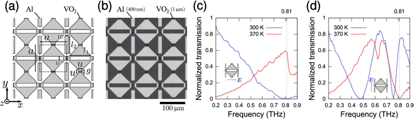
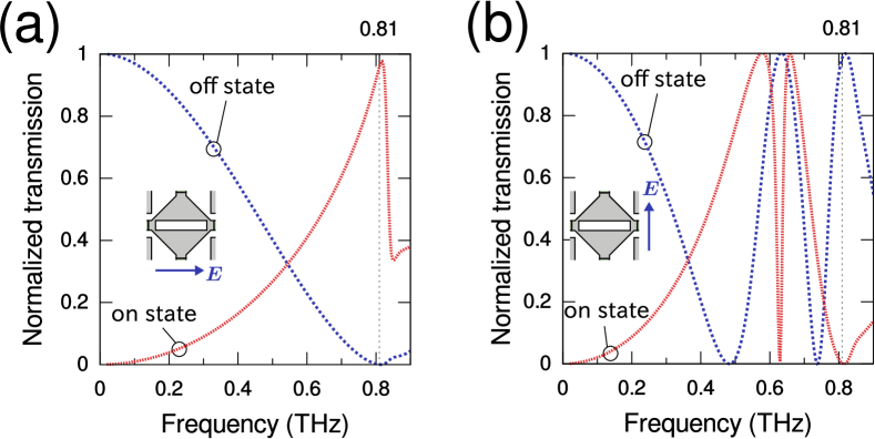
Now, we consider the experimental demonstration of a reconfigurable D-checkerboard in the terahertz frequency range. For the variable-resistance sheets, we use vanadium dioxide (VO2) on a c-cut sapphire substrate. As the temperature increases above , VO2 exhibits an insulator-to-metal transition where the electrical conductivity typically changes by several orders of magnitude; thus, the metasurface transitions from the off state to the on state. Using the c-cut sapphire as a substrate at causes mirror symmetry breaking with respect to where the structures are located, and the condition for Babinet’s principle is no longer satisfied. In the target terahertz frequency range, c-cut sapphire has a refractive index and Grischkowsky et al. (1990). To compensate this substrate effect, we must modify the design of the D-checkerboard, as shown in Fig. 4(a). In the following discussion, we use the normalized transmission coefficient of the metasurface with a sapphire substrate as for an -polarized normally incident wave, where is the amplitude transmission coefficient of the plane with metasurface from air to the substrate, and is the Fresnel coefficient for transmission from air to the sapphire. For -polarized normally incident waves, we changed the gap to ensure and Urade et al. (2016b), where is the modified resonant angular frequency. For -polarized normally incident waves, we use different lengths for the dipoles and their complements. By optimizing these parameters, we obtain and to realize and . The calculated transmission spectra of the designed metasurface are shown in Fig. 7 of the Appendix.
Next, we experimentally demonstrate dynamic rotation of the transmitting axis of the reconfigurable metasurface. The designed D-checkerboard is fabricated as follows. A thin film of stoichiometric VO2 of about 1- thickness is deposited on a sapphire (0001) substrate (thickness: ) via reactive magnetron sputtering of a vanadium target Okimura et al. (2006). After a positive photoresist is patterned on the VO2 using a maskless lithography technique, the unnecessary part of the VO2 film is removed by wet etching. The D-checkerboard made of aluminum (thickness: ) is formed by photolithography and electron beam evaporation at room temperature and lift-off techniques. A micrograph of the fabricated sample is shown in Fig. 4(b). The squares with target side length are partially overlapped by the Al structures, for ensuring electrical connection. The maximum thickness of the device fabricated on a c-cut sapphire substrate is , which is deep subwavelength compared with the wavelength at the target frequency.
To evaluate the D-checkerboard, we use a conventional terahertz time-domain spectroscopy system. To delay the signals reflected at the boundaries, two pieces of c-cut sapphire substrates of thickness are attached under the metasurface with a c-cut sapphire substrate. Therefore, the overall thickness of the substrate is . A reference c-cut sapphire sample with thickness is prepared by stacking three sapphire plates of thickness . The stacked samples are held by a brass holder with a temperature feedback system to control the electric current in a nichrome wire attached to the holder, while the temperature of the holder is monitored by a thermocouple. A collimated terahertz beam with a linear polarization and beam diameter is normally incident onto the stacked samples. The temporal profile of the electric field is measured using a detector dipole antenna. The multiple reflected signal is cut using a time-domain window function. Measuring the electric fields of the c-cut reference sapphire substrate and , we calculate the normalized complex amplitude transmission coefficient , where and are Fourier transformed electric fields. Figures 4(c) and (d) show the power transmission spectra of the D-checkerboard on a sapphire substrate for normal incidence of collimated terahertz beams with and polarization, respectively. The lowest diffraction frequency of the D-checkerboard is given by . At , the dynamic rotation of the transmitting axis of the metasurface from the axis to the axis is realized by heating the device. The extinction ratios and at are . Although the frequency dependences of the transmission spectra agree well with the simulated data shown in Fig. 7 of the Appendix, the maximum transmission peaks of the on- and off-state metasurface are not as high as the simulated data. This is because the resistivity of the VO2 film is not switched ideally and the aluminum has a finite conductivity. High quality vanadium-dioxide films formed by other deposition techniques, such as pulse laser deposition Nag and Haglund Jr (2008), and higher conductive metals could improve the performance of the device.
IV Conclusion
In this paper, we introduced the class of anisotropic Babinet-invertible metasurfaces enabling transmission–reflection switching for each orthogonally polarized wave, and experimentally demonstrated their applicability to polarization control of electromagnetic waves. The transmission inversion for each orthogonal polarization can be considered as a manifestation of an artificially engineered insulator–metal transition of anisotropic metasurfaces. The concept of anisotropic Babinet-invertible metasurfaces enabling transmission–reflection switching for each orthogonally polarized wave is universal, and is independent of the implementation. Their applications are not limited to reconfigurable terahertz polarizers, but could find a wide range of applications for dynamic polarization control over a broad region of the electromagnetic spectrum in which the variable-resistance materials can be used. Ultrafast switching could be realized if photoexcitation of carriers is employed. Thus, the anisotropic Babinet-invertible metasurfaces will pave the way for ultra-fast polarization-selective spectroscopy.
Acknowledgments
The authors gratefully acknowledge the contributions of T. Nishida and T. McArthur. The sample fabrication was performed with the help of Kyoto University Nano Technology Hub, as part of the “Nanotechnology Platform Project” sponsored by MEXT, Japan. The present research is supported by grant from the Murata Science Foundation and JSPS KAKENHI Grant Number JP16K13699. One of the authors (Y.U.) was supported by a JSPS Research Fellowship for Young Scientists.
Appendix A Multimode formation in D-checkerboard
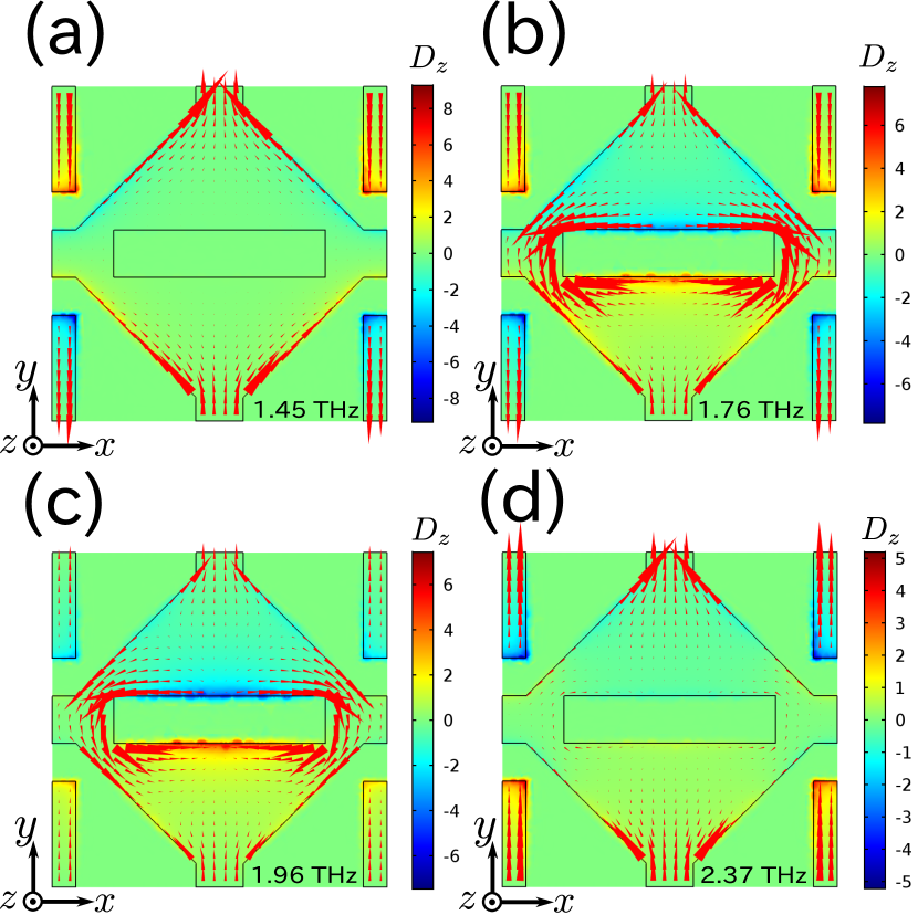
Here, we investigate the formation of the multiple resonances of an ideal D-checkerboard. The field distributions of on- and off-state metasurfaces are exactly related to each other, so we focus only on the on-state metasurface. We first study the transmission spectra and field distribution of each component of the ideal D-checkerboard in a vacuum by COMSOL using the parameters for an ideal D-checkerboards shown in Fig. 2(b): , , and . Periodic boundary conditions are applied at the sides of the unit cell, and ports with only lowest frequency modes are set on the bottom and top faces. The metallic structures are assumed to be zero-thickness perfect electric conductors. Normally incident -polarized plane waves enter the metasurface at from to . Figure 5(a) shows the transmission spectra of the dipoles and the on-state checkerboard. The dipoles and the on-state checkerboard show a transmission dip at and transmission peak at . The electric displacement just above the surface (), corresponding to the charge density, and the surface current distributions on the metal () at these frequencies, are shown in Figs. 5(b) and (c). To clearly see the distributions, the phase of is shifted by compared with the surface current in these plots. The first-order resonance of the dipoles is shown in Fig. 5(b). In Fig. 5(c), the direction of the surface current at the center of the on-state checkerboard is opposite that on the top and bottom interconnection patches.
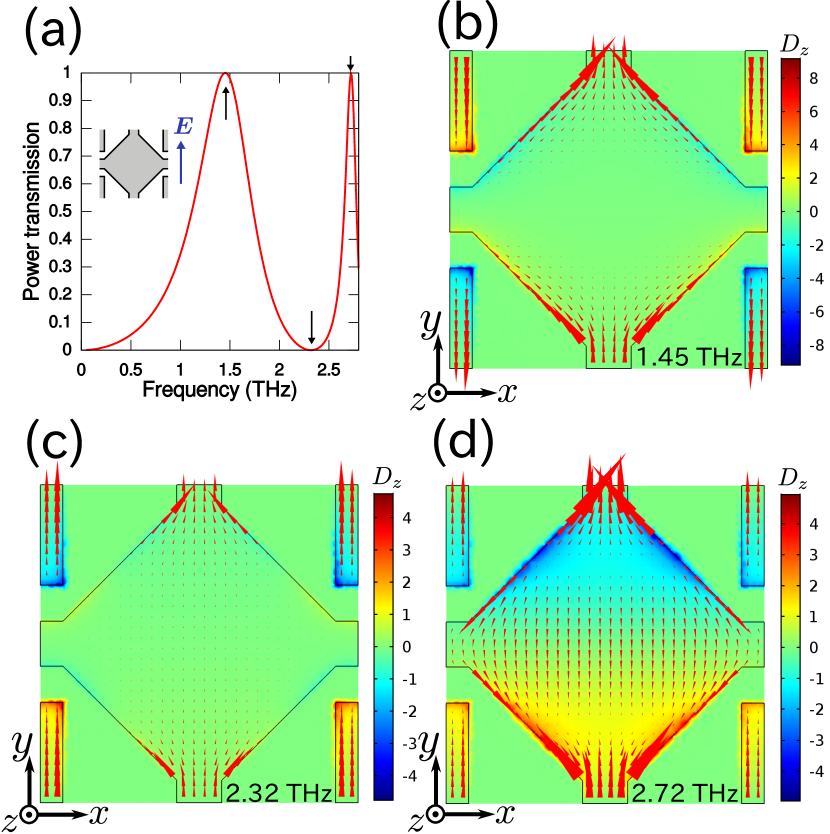
Next, we consider the on-state checkerboard combined with dipoles. The spectrum of the on-state checkerboard with dipoles at the normal incidence of -polarized plane waves is shown in Fig. 6(a). It shows Fano-like characteristics Miroshnichenko et al. (2010) with transmission peaks at and , and a transmission dip at . The charge and surface current distribution on the dipoles at [Fig. 6(b)] and [Fig. 6(c)] are similar to those shown in Fig. 5(b). At these frequencies, the phase relations between the currents on the checkerboard and the dipole are opposite, and the resonant transmission at and reflection at are caused by interference between the first-order dipole mode and the on-state checkerboard mode. The current distributions on the checkerboard and the dipole at in Fig. 6(d) are similar to those in Fig. 5(b) and (c), respectively. This indicates that the resonant transmission originates from a hybridized mode of the first-order dipole mode and on-state checkerboard mode.
Appendix B Simulation for modified D-checkerboard on a c-cut sapphire substrate
Here, we present spectra of a modified D-checkerboard on a c-cut sapphire substrate. The geometrical parameters are , , , , and . We assume that all conductive parts are zero-thickness perfect electric conductors. The calculation is performed in the unit cell and periodic boundary conditions are imposed on the sides. The metallic structures are located on . A linearly-polarized plane wave is generated from a PML (perfectly matched layer)-backed port with a slit condition on the interior port, and detected by another port with the similar setting. The refractive index of the c-cut sapphire is set to be and . The calculated normalized power transmission spectra are shown in Fig. 7.
References
- Solymar and Shamonina (2009) L. Solymar and E. Shamonina, Waves in Metamaterials (Oxford University Press, New York, 2009).
- Kildishev et al. (2013) A. V. Kildishev, A. Boltasseva, and V. M. Shalaev, Planar Photonics with Metasurfaces, Science 339, 1232009 (2013).
- Monticone et al. (2013) F. Monticone, N. M. Estakhri, and A. Alù, Full Control of Nanoscale Optical Transmission with a Composite Metascreen, Phys. Rev. Lett. 110, 203903 (2013).
- Pfeiffer and Grbic (2013) C. Pfeiffer and A. Grbic, Metamaterial Huygens’ Surfaces: Tailoring Wave Fronts with Reflectionless Sheets, Phys. Rev. Lett. 110, 197401 (2013).
- Tao et al. (2011) H. Tao, W. J. Padilla, X. Zhang, and R. D. Averitt, Recent Progress in Electromagnetic Metamaterial Devices for Terahertz Applications, IEEE J. Sel. Topics Quantum Electron. 17, 92 (2011).
- Booker (1946) H. Booker, SLOT AERIALS AND THEIR RELATION TO COMPLEMENTARY WIRE AERIALS (BABINET’S PRINCIPLE), J. IEE (London), part IIIA 93, 620 (1946).
- Note (1) Rigorously, the sheet impedance is defined as , for the tangential component of the electric field on and surface current density on . Here, is an angular frequency and “c.c.” represents the complex conjugate operation.
- Baum and Singaraju (1974) C. E. Baum and B. K. Singaraju, Generalization of Babinet’s Principle in Terms of the Combined Field to Include Impedance Loaded Aperture Antennas and Scatterers, Interaction Note No.217 (Air Force Weapons Lab., Kirtland Air Force Base, NM 87117) (1974).
- Compton et al. (1984) R. C. Compton, J. C. Macfarlane, L. B. Whitbourn, M. M. Blanco, and R. C. McPhedran, Babinet’s principle applied to ideal beam-splitters for submillimetre waves, Opt. Acta 31, 515 (1984).
- Kempa (2010) K. Kempa, Percolation effects in the checkerboard Babinet series of metamaterial structures, Phys. Status Solidi Rapid Res. Lett. 4, 218 (2010).
- Edmunds et al. (2010) J. D. Edmunds, A. P. Hibbins, J. R. Sambles, and I. J. Youngs, Resonantly inverted microwave transmissivity threshold of metal grids, New J. Phys. 12, 063007 (2010).
- Takano et al. (2014) K. Takano, F. Miyamaru, K. Akiyama, H. Miyazaki, M. W. Takeda, Y. Abe, Y. Tokuda, H. Ito, and M. Hangyo, Crossover from capacitive to inductive electromagnetic responses in near self-complementary metallic checkerboard patterns, Opt. Express 22, 24787 (2014).
- Ramakrishna et al. (2011) S. A. Ramakrishna, P. Mandal, K. Jeyadheepan, N. Shukla, S. Chakrabarti, M. Kadic, S. Enoch, and S. Guenneau, Plasmonic interaction of visible light with gold nanoscale checkerboards, Phys. Rev. B 84, 245424 (2011).
- González-Ovejero et al. (2015a) D. González-Ovejero, E. Martini, B. Loiseaux, C. Tripon-Canseliet, M. J. Mencagli, J. Chazelas, and S. Maci, Basic Properties of Checkerboard Metasurfaces, IEEE Antennas Wireless Propag. Lett. 14, 406 (2015a).
- González-Ovejero et al. (2015b) D. González-Ovejero, E. Martini, and S. Maci, Surface Waves Supported by Metasurfaces With Self-Complementary Geometries, IEEE Trans. Antennas Propag. 63, 250 (2015b).
- Tremain et al. (2015) B. Tremain, C. J. Durrant, I. E. Carter, A. P. Hibbins, and J. R. Sambles, The Effect of Rotational Disorder on the Microwave Transmission of Checkerboard Metal Square Arrays, Sci. Rep. 5, 16608 (2015).
- Nakata et al. (2013) Y. Nakata, Y. Urade, T. Nakanishi, and M. Kitano, Plane-wave scattering by self-complementary metasurfaces in terms of electromagnetic duality and Babinet’s principle, Phys. Rev. B 88, 205138 (2013).
- Urade et al. (2015) Y. Urade, Y. Nakata, T. Nakanishi, and M. Kitano, Frequency-Independent Response of Self-Complementary Checkerboard Screens, Phys. Rev. Lett. 114, 237401 (2015).
- Urade et al. (2016a) Y. Urade, Y. Nakata, T. Nakanishi, and M. Kitano, Broadband and energy-concentrating terahertz coherent perfect absorber based on a self-complementary metasurface, Opt. Lett. 41, 4472 (2016a).
- Note (2) Note that the complex amplitude transmission coefficient from an incident wave to a transmitted wave is defined by . In this paper, the modifier zeroth-order represents the case that satisfies , where is the projection operator onto (: transpose).
- Urade et al. (2016b) Y. Urade, Y. Nakata, K. Okimura, T. Nakanishi, F. Miyamaru, M. W. Takeda, and M. Kitano, Dynamically Babinet-invertible metasurface: a capacitive-inductive reconfigurable filter for terahertz waves using vanadium-dioxide metal-insulator transition, Opt. Express 24, 4405 (2016b).
- van der Valk et al. (2005) N. C. J. van der Valk, W. A. M. van der Marel, and P. C. M. Planken, Terahertz polarization imaging, Opt. Lett. 30, 2802 (2005).
- Katletz et al. (2012) S. Katletz, M. Pfleger, H. Pühringer, M. Mikulics, N. Vieweg, O. Peters, B. Scherger, M. Scheller, M. Koch, and K. Wiesauer, Polarization sensitive terahertz imaging: detection of birefringence and optical axis, Opt. Express 20, 23025 (2012).
- Grischkowsky et al. (1990) D. Grischkowsky, S. Keiding, M. van Exter, and C. Fattinger, Far-infrared time-domain spectroscopy with terahertz beams of dielectrics and semiconductors, J. Opt. Soc. Am. B 7, 2006 (1990).
- Okimura et al. (2006) K. Okimura, Y. Sasakawa, and Y. Nihei, X-ray Diffraction Study of Electric Field-Induced Metal–Insulator Transition of Vanadium Dioxide Film on Sapphire Substrate, Jpn. J. Appl. Phys. 45, 9200 (2006).
- Nag and Haglund Jr (2008) J. Nag and R. F. Haglund Jr, Synthesis of vanadium dioxide thin films and nanoparticles, J. Phys.: Condens. Matter 20, 264016 (2008).
- Miroshnichenko et al. (2010) A. E. Miroshnichenko, S. Flach, and Y. S. Kivshar, Fano resonances in nanoscale structures, Rev. Mod. Phys. 82, 2257 (2010).