NanoSQUIDs: Basics & recent advances
Abstract
Superconducting Quantum Interference Devices (SQUIDs) are one of the most popular devices in superconducting electronics. They combine the Josephson effect with the quantization of magnetic flux in superconductors. This gives rise to one of the most beautiful manifestations of macroscopic quantum coherence in the solid state. In addition, SQUIDs are extremely sensitive sensors allowing to transduce magnetic flux into measurable electric signals. As a consequence, any physical observable that can be converted into magnetic flux, e.g., current, magnetization, magnetic field or position, becomes easily accessible to SQUID sensors. In the late 1980’s it became clear that downsizing the dimensions of SQUIDs to the nanometric scale would encompass an enormous increase of their sensitivity to localized tiny magnetic signals. Indeed, nanoSQUIDs opened the way to the investigation of, e.g., individual magnetic nanoparticles or surface magnetic states with unprecedented sensitivities. The purpose of this review is to present a detailed survey of microscopic and nanoscopic SQUID sensors. We will start by discussing the principle of operation of SQUIDs, placing the emphasis on their application as ultrasensitive detectors for small localized magnetic signals. We will continue by reviewing a number of existing devices based on different kinds of Josephson junctions and materials, focusing on their advantages and drawbacks. The last sections are left for applications of nanoSQUIDs in the fields of scanning SQUID microscopy and magnetic particle characterization, putting special stress on the investigation of individual magnetic nanoparticles.
I Introduction
The superconducting quantum interference device (SQUID) consists of a superconducting ring intersected by one (rf SQUID) or two (dc SQUID) Josephson junctions. SQUIDs constitute, still at present, the most sensitive sensors for magnetic flux in the solid state Clarke and Braginski (2004); Kleiner et al. (2004). For more than 50 years, a plethora of devices exploiting this property have been envisioned, fabricated and used in many fields of applications Clarke and Braginski (2006). These devices include voltmeters, current amplifiers, metrology standards, motion sensors and magnetometers. One of the key applications of SQUIDs is in magnetometry. Here, a superconducting input circuit (flux transformer) picks up the magnetic flux density , captured by superconducting pick-up loops of some mm2 or cm2 area, and the induced current is then (typically inductively) coupled to a SQUID. The figure of merit of SQUID magnetometers is the field resolution , which can reach values down to about . Here, is the spectral density of flux noise of the SQUID and is the effective area of the magnetometer.
To ensure good coupling from an input circuit to a SQUID, typically thin film multiturn input coils are integrated on top of a washer-type SQUID loop. Typical thin film washer SQUIDs have lateral outer dimensions of several m, the inner hole size is several tens of m and the lateral size of the Josephson junctions is several m. Such devices are fabricated by conventional thin film technology, including micropattering by photolithography. With the development of a mature junction technology, based on sandwich-type Nb/Al-AlOx/Nb junctions in the 1980s Gurvitch et al. (1983), Nb based dc SQUIDs became the most commonly used type of devices for various applications. At the same time, first attempts were started to further miniaturize the lateral dimensions of SQUIDs, including the Josephson junctions Voss et al. (1980). This was made possible by advances in nanolithography Broers et al. (1976) and was motivated by the development of the theory for thermal noise in the dc SQUID Tesche and Clarke (1977), which showed that the energy resolution of dc SQUIDs can be improved by reducing the SQUID loop inductance and junction capacitance , to eventually reach and explore quantum limited resolution of such devices Koch et al. (1981). These developments have triggered the realization of miniaturized dc SQUIDs for the investigating of small magnetic particles and for imaging of magnetic field distributions by scanning SQUID microscopy to combine high sensitivity to magnetic flux with high spatial resolution. In 1984, Ketchen et al. Ketchen et al. (1984) presented the first SQUID microsusceptometer devoted to detect the tiny signal produced by micron-sized magnetic objects, and in 1983 Rogers and Bermon developed the first system to produce 2-dimensional scans of magnetic flux structures in superconductors Rogers (1983). Both developments were pushed further in the 1990s. Wernsdorfer et al. Wernsdorfer et al. (1995a); Wernsdorfer (2001) used micron-sized SQUIDs to perform experiments on the magnetization reversal of nanometric particles, which were placed directly on top of the SQUIDs. At the same time, scanning SQUID microscopes with miniaturized SQUIDs and/or pickup loop structures have been developed, at that time with focus on studies on the pairing symmetry in the high transition temperature (high-) cuprate superconductors Kirtley (2010). Since then much effort has been dedicated to the further miniaturization of SQUID devices and to the optimization of their noise characteristics Granata and Vettoliere (2016).
Studies on the properties of small spin systems, such as magnetic nanoparticles (MNPs) and single molecule magnets (SMMs), have fueled the development of new magnetic sensors for single particle detection and imaging with improved performance. Many of the recent advances in this field include the development of magneto-optical techniques based on nitrogen vacancy centers in diamond Schäfer-Nolte et al. (2014); Thiel et al. (2016) or the use of carbon nanotubes (CNTs) as spin detectors Ganzhorn et al. (2013). Alternatively, miniature magnetometers, based on either microHall bars Lipert et al. (2010) or micro- and nanoSQUIDs, provide direct measurement of the stray magnetic fields generated by the particle under study, making the interpretation of the results much more direct and simple. While their sensitivity deteriorates rapidly when Hall sensors are reduced to the submicron size, miniaturized SQUID-based sensors can theoretically reach quantum limited resolution.
In this review, we give an overview on some basics of nanoSQUIDs 111The term nanoSQUID denotes strongly miniaturized thin film SQUIDs with lateral dimensions in the submicrometer range. However, some devices described here and also various statements made also refer to slightly larger structures, which sometimes are denoted as microSQUIDs. Throughout the text, we do not make this discrimination. and recent advances in the field. After a brief description of some SQUID basics in section II, we will review in section III important design considerations for optimizing nanoSQUID performance and the state of the art in fabrication and performance of nanoSQUIDs based on low- and high- superconductors, with emphasis on the various types of Josephson junctions used. Subsequently, we will review important applications of nanoSQUIDs, divided into two sections: Section IV gives an overview on applications of nanoSQUIDs for magnetic particle detection, and section V addresses nanoSQUIDs for scanning SQUID microscopy. We will conclude with a short section VI, which gives a summary and outlook.
II SQUIDs: some basic considerations
The working principle of a SQUID is based on two fundamental phenomena in superconductors, the fluxoid quantization and the Josephson effect. The fluxoid quantization arises from the quantum nature of superconductivity, as the macroscopic wave function describing the whole ensemble of Cooper pairs shall not interfere destructively. This leads to the quantization of the magnetic flux threading a superconducting loop London (1950), in units of the magnetic flux quantum Vs.
The Josephson effect Josephson (1962); Anderson and Rowell (1963) results from the overlap of the macroscopic wave functions between two superconducting electrodes at a weak link forming the Josephson junction (JJ). The supercurrent through the weak link and the voltage drop across it satisfy the Josephson relations
| (1) |
with the gauge-invariant phase difference between the macroscopic wave functions of both superconductors and the maximum attainable supercurrent ; the dot refers to the time derivative. The simple sinusoidal current-phase relation (CPR), Eq. (1(a)), is found for many kinds of JJs. However, some JJ types exhibit a non-sinusoidal CPR, which can even be multivalued Likharev (1979).
II.1 Resistively and capacitively shunted junction model

A very useful approach to describe the phase dynamics of a JJ is the resistively and capacitively shunted junction (RCSJ) model Stewart (1968); McCumber (1968); Chesca et al. (2004). Within this model, the current flow is split into three parallel channels [Fig. 1(a)]: (i) a supercurrent [Eq. (1(a))], (ii) a dissipative quasiparticle current across an ohmic resistor and (iii) a displacement current across the junction capacitance . A finite temperature is included as a thermal current noise source from the resistor. With Kirchhoff’s law and Eq. (1(b)), one obtains the equation of motion for the phase difference
| (2) |
This is equivalent to the equation of motion of a point-like particle moving in a tilted washboard potential [Fig. 1(b)]
| (3) |
with normalized currents , and the Josephson coupling energy . In this analogy, the mass, friction coefficient, driving force (tilting the potential) and velocity correspond to , , and , respectively. Hysteresis in the current voltage characteristics (IVC), i.e. bias current vs time averaged voltage , can be understood as a consequence of the particle’s inertia: the dissipative state is achieved once the metastable minima of the washboard potential disappear at . If is decreased from , the particle becomes retrapped at , leading to a hysteretic IVC. This behavior can be quantified by the Stewart-McCumber parameter
| (4) |
In order to obtain a non-hysteretic IVC, must be kept below . This can be e.g. achieved by means of an additional shunt resistor, parallel to the JJ.
II.2 dc SQUID basics
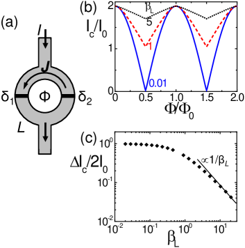
The dc SQUID Jaklevic et al. (1964) is a superconducting loop (with inductance ) intersected by two JJs [Fig. 2(a)]. With an externally applied magnetic flux through the loop, the fluxoid quantization links the phase differences and of the two JJs to the total flux in the SQUID via
| (5) |
Here, is the current circulating in the SQUID loop and is an integer Kleiner and Koelle (2004). Defining the screening parameter as
| (6) |
one finds in the limit a negligible contribution of to in Eq. (5), and by assuming for simplicity identical values for in the two JJs, the maximum supercurrent (critical current) of the SQUID can be easily obtained as
| (7) |
The pronounced dependence [Fig. 2(b) for ] can be used to probe tiny changes in applied magnetic flux. No analytical expression for can be obtained when a finite and hence a finite is included, unless restrictions are imposed to some of the important SQUID parameters Chesca et al. (2004); Soloviev et al. (2016). An increasing leads to a monotonic decrease of the critical current modulation with increasing [Fig. 2(b,c)]. This effect allows to estimate from the measured .
We note that the inductance has two contributions Kleiner and Koelle (2004): The geometric inductance relates the induced flux to the current circulating in the SQUID loop. The kinetic inductance is due to the kinetic energy of and can often be neglected; however, it becomes significant when the width and/or thickness of the SQUID ring are comparable to or smaller than the London penetration depth .
For most applications, the dc SQUID is operated in the dissipative state as a flux-to-voltage transducer. In this case, the SQUID is current biased slightly above , leading to a -periodic modulation of , which is often sinusoidal. This mode of operation requires non-hysteretic IVCs, i.e., . An applied flux signal causes then a change in SQUID voltage, which for small enough signals is given by . Usually, the working point (with respect to bias current and applied bias flux) is chosen such that the slope of the curve is maximum, which is denoted as the transfer function .
The sensitivity of the SQUID in the voltage state is limited by voltage fluctuations, which are quantified by the spectral density of voltage noise power . This is converted into an equivalent spectral density of flux noise power or the rms flux noise with units [Fig. 3(a)].
At low frequency , excess noise scaling typically as (1/ noise) shows up. Major sources are critical current fluctuations in the JJs and thermally activated hopping of Abrikosov vortices in the superconducting film, which is particularly strong in SQUIDs based on the high- cuprate superconductors Koelle et al. (1999). Moreover, noise has also been ascribed to flux noise arising from fluctuating spins at the interfaces of the devices Koch et al. (2007). This is supported by the observation of a paramagnetic signal following a Curie-like -dependence Sendelbach et al. (2008); Bluhm et al. (2009); Martínez-Pérez et al. (2011a). However, a complete description of noise is still missing.
At higher frequencies, becomes indepenent of . This white noise is mainly due to Johnson-Nyquist noise associated with dissipative quasiparticle currents in the JJs or shunt resistors. Within a Langevin approach, the thermal noise is described by two independent fluctuation terms in the coupled equations of motion for the two RCSJ-type JJs. Numerical simulations yield vs , and the noise parameter Koelle et al. (1999); Chesca et al. (2004). For , and , one finds
| (8) |
For , increases again with decreasing . Typically, SQUIDs are designed to give , for which Eq. (8) reduces to Tesche and Clarke (1977). This linear scaling , however, saturates in the sub-Kelvin range [Fig. 3(b)] due to the hot-electron effect stemming from limited electron-phonon interaction at low Wellstood et al. (1994). We note that (for fixed ), meaning that small loop inductances yield lower white flux noise levels. Other sources of white noise are shot and quantum noise, lying usually below the Johnson-Nyquist term. For the case , the former is given by Tesche and Clarke (1977), whereas the latter arises from zero point quantum fluctuations giving Koch et al. (1981).
II.3 SQUID readout
II.3.1 Flux-locked loop
The periodic response of the SQUID to magnetic flux can be linearized to obtain a larger dynamic range. This can be achieved by operation in the flux locked loop (FLL) mode Drung and Mück (2004). Here, the SQUID is (typically current) biased at an optimum working point and behaves as a null-detector of magnetic flux. A small variation of the external flux changes the SQUID output (typically a voltage change ). This small deviation from the working point is amplified, integrated, and fed back to the SQUID via a current through a feedback resistor and coil, which is inductively coupled to the SQUID. The output voltage across is then proportional to the flux signal . The dynamic response in FLL mode is limited by the slew rate, i.e. the speed at which the feedback circuit can compensate for rapid flux changes at the input. Under optimum conditions, the bandwidth of the FLL is only limited by propagation delays between the room temperature feedback electronics and the SQUID; a typical distance of 1 m yields MHz.
II.3.2 Voltage readout
The most simple SQUID readout uses current biased operation in the dissipative state; as mentioned above, the IVCs should be non-hysteretic in this case. As the transfer function is typically small (several ), the voltage noise at the output can easily be dominated by room-temperature amplifier noise. To circumvent this problem, one can use a flux modulation scheme Drung and Mück (2004). Here, the SQUID is flux-modulated by an ac signal (amplitude , frequency kHz), and the resulting ac voltage across the SQUID is amplified with a (cold) step-up transformer to increase the SQUID signal and noise. The modulated SQUID response is further amplified at room temperature and lock-in detected. Suitable electronics achieve a bandwidth of up to 100 kHz.
In a different approach, one can increase by additional positive feedback (APF), which distorts the characteristics and increases at the positive slope. This enables simple direct readout of the SQUID signal Drung and Mück (2004). Alternatively, a low-noise SQUID or serial SQUID array (SSA) amplifier can be used to amplify the SQUID voltage at low in a two-stage readout configuration.
II.3.3 Critical current readout & threshold detection
For SQUIDs with hysteretic IVCs one can exploit the modulation directly. In this case one ramps the bias current until the SQUID switches to the dissipative state, producing a voltage drop. At this point the current is switched off, and is calculated from the duration of the ramp Wernsdorfer (2009). This technique can also be used with a FLL scheme Wernsdorfer (2009); Russo et al. (2012); Granata et al. (2013a). Sensitivity is limited by the accuracy in determining , which is described by the escape of a particle from a potential minimum. Such a process can be thermally activated or quantum driven and is strongly influenced by electronic noise. Hence, a large number of switching events is needed to obtain sufficient statistics.
To minimize Joule heating, the SQUID can be operated as a threshold sensor. Here, the SQUID is current-biased very close to the switching point. If the magnetic flux threading the loop changes abruptly, the SQUID is triggered to the dissipative state and a voltage drop will be measured Wernsdorfer (2009).
Both techniques were applied to magnetization reversal measurements on MNPs in sweeping magnetic fields Wernsdorfer (2009). For measurements up to large , applied along any direction, the measurement procedure is divided into three steps. First, is applied to saturate the particle’s magnetization along any direction. Second, is swept along the opposite direction to a value and back to zero. To check whether this reversed the particle’s magnetization, an in-plane field sweep is done as a third step. If the particle’s magnetization reversal is (not) detected in the third step one can conclude that was above (below) the switching field . These steps can be repeated several times to determine precisely. Note that the second step can be performed above of the SQUID. Rather than tracing out full loops, this technique can be used to trace out the dependence of on the field direction and temperature Jamet et al. (2001).
II.3.4 Dispersive read out
So far, we discussed SQUID operation in the voltage state or close to it. Such schemes entail dissipation of Joule power that might affect the state of the magnetic system under study. An elegant way to circumvent this problem is the operation of the SQUID as a flux-dependent resonator; this has also the advantage of increasing enormously the bandwidth up to MHz Hatridge et al. (2011); Levenson-Falk et al. (2013). The SQUID is always in the superconducting state and acts as a flux-dependent inductance connected in parallel to a capacitor. The resonance frequency of the circuit depends on the total flux threading the SQUID loop. This can be read out by conventional microwave reflectometry giving a direct flux-to-reflected phase conversion. The devices are operated in the linear regime, i.e., using low-power driving signals. To determine the spectral density of flux noise, the overall voltage noise of the circuit is estimated and scaled with the transduction factor . The noise performance can be boosted considerably by taking advantage of the CPR non-linearity, i.e., operating the nanoSQUID as a parametric amplifier. For this purpose, the driving power is increased so that the resonance peak is distorted, giving a much sharper dependence of the reflected phase on .
III nanoSQUIDs: design, fabrication & performance
NanoSQUIDs are developed for detecting small spin systems, such as MNPs or SMMs, or for high-resolution imaging of magnetic field structures by SQUID microscopy. For such applications, the figure of merit is the spin sensitivity, which can be boosted down to the level of a single electron spin. The use of strongly miniaturized SQUID loops and JJs is based on the following ideas:
-
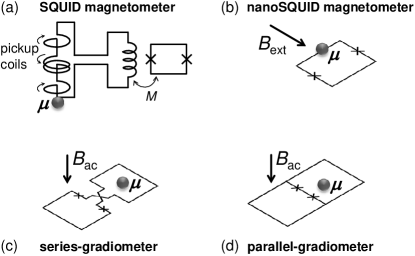
Stronlgy localized magnetic field sources (e.g. MNPs) are placed in close vicinity to the SQUID, instead of using pickup coils [Fig. 4(a)] which degrade the overall coupling. A single SQUID loop [Fig. 4(b)] can be used to detect the magnetic moment of a MNP, or gradiometric configurations [Fig. 4(c,d)] enable measurements of the magnetic ac susceptibility .
-
The coupling of the stray field from local field sources to the nearby SQUID can be improved by reducing the cross section (width and thickness) of the superconducting thin film forming the SQUID loop (see section III.1).
-
The sensitivity of the SQUID to magnetic flux (magnetic flux noise in the thermal white noise limit) can be improved by reducing the loop inductance, i.e. by shrinking the lateral size of the SQUID loop (see section III.1).
-
For magnetization reversal measurements on MNPs, an external field is applied ideally exactly in the plane of the SQUID loop to switch the MNP’s magnetization (see section IV.2), albeit without coupling flux directly to the loop. By reducing the dimensions of the JJs and the loop, the nanoSQUID can be made less sensitive to for small misalignment of .
-
Reducing the loop size together with the SQUID-to-sample distance can significantly boost the spatial resolution for scanning SQUID microscopy applications (see section V).
III.1 nanoSQUIDs: design considerations
The ability of a nanoSQUID to resolve tiny signals from the magnetic moments of small spin systems depends (i) on the intrinsic flux noise of the SQUID and (ii) on the amount of flux which a particle with magnetic moment couples to the SQUID loop. The latter can be quantified by the coupling factor , with . As a result, one can define the spin sensitivity , with units ; is the Bohr magneton. expresses the minimum magnetic moment that can be resolved per unit bandwidth. Hence, optimizing nanoSQUID performance requires to minimize while maximizing .
As mentioned in section II.2, has typically a low-frequency 1/-like contribution and a thermal white noise part . The 1/ contribution is hard to optimize by design; however, depends on geometrical parameters through the loop inductance , but also on junction parameters such as , and . The dependence (Eq.(8)) implies that can be improved by decreasing via the loop dimensions, while considering the constraints on and , which will affect the choice of junction parameters. Such an optimization procedure can be tested experimentally by performing flux noise measurements of the SQUIDs.
The optimization of the coupling factor is more difficult. It is defined as the magnetic flux coupled to the SQUID loop by the magnetic dipole field of a point-like particle, divided by its magnetic moment . The magnitude of depends on SQUID geometry, particle position (relative to the SQUID) and orientation of its magnetic moment. This quantity is not directly accessible by experiments, and one has to rely on estimates, analytic approximations or numerical calculations for determining and optimizing it.
To the best of our knowledge, Ketchen et al. Ketchen et al. (1989) were the first to give an estimate of . For a magnetic dipole at the center of an infinitely thin loop with radius , with along the loop normal
| (9) |
was found. 222 in cgs units, as derived by Ketchen et al. Ketchen et al. (1989). The spin sensitivity in Ketchen et al. (1989) relates to our definition as , i.e. has the units of number of spins (of moment ) per . The r.h.s. of Eq. (9) is obtained with the definition of the classical electron radius , and , which yields .
The coupling improves if the particle is moved close to the loop’s banks Bouchiat (2009). However, a quantitative estimate of is more difficult in this near-field regime Tilbrook (2009), as the cross-section of the SQUID banks and the flux focusing effect caused by the superconductor must be taken into account. The calculation of requires calculating the magnetic field distribution at the position of the SQUID, originating from a magnetic moment at position , and from this the magnetic flux coupled to the SQUID. This problem can be simplified by exploiting the fact that sources and fields can be interchanged, i.e., one evaluates the magnetic field , created by a circulating supercurrent through the SQUID loop, at the position of the magnetic dipole. With the normalized quantity , which does not depend on , one finds Bouchiat (2009); Nagel et al. (2011a)
| (10) |
This allows to calculate for any position and orientation of the magnetic dipole in 3D space once is known. 333The current through an infinitely thin wire, forming a loop with radius in the plane and centered at the origin, induces a field , at the center of the loop. Hence, for a magnetic dipole placed at the origin and pointing in direction, , Eq. (10) yields , i.e. the same result as derived by Ketchen et al. Ketchen et al. (1989).
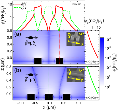
The normalized field has to be determined from the spatial distribution of the supercurrent density circulating in the SQUID loop, which depends only on the SQUID geometry and on . This has been done for various types of nanoSQUIDs by numerically solving the London equations Nagel et al. (2011a, b, 2013); Schwarz et al. (2013, 2015); Wölbing et al. (2013, 2014). Numerical simulations of reveal that the coupling can be increased in the near-field regime if the magnetic dipole is placed as close as possible on top of a constriction in the SQUID loop, which is as thin and narrow as possible Wölbing et al. (2014). Typical have been obtained for magnetic dipoles at 10 nm distance from a constriction (nm wide and thick) in YBa2Cu3O7 (YBCO) nanoSQUIDs. 444 depends significantly on the loop width, thickness and . For example for a dipole centered at a circular SQUID loop with inner radius nm, outer radius m, and nm one finds , i.e. a factor 1.6 smaller as obtained from Ref. Ketchen et al. (1989) (with nm); decreases further with decreasing ratio . Simulation results for two types of Nb nanoSQUIDs [Fig. 5] show that the dipole has to approach the SQUID surface closely to reach values above a few n (see linescans in the right graphs in Fig. 5). The linescans (top graph in Fig. 5) show that the coupling is maximum right above the loop structures Nagel et al. (2011b).
Measurements on spatially extended magnetic systems, such as a Ni nanotube Nagel et al. (2013) or a Fe nanowire Schwarz et al. (2015), were found to be consistent with the numerical approach described above. This was done by comparing the measured flux coupled to nanoSQUIDs from fully saturated tubes or wires with the calculated flux signals, obtained by integrating over the finite volume of the sample. First measurements on the SQUID response as a function of the position of a magnetic sample have been reported earlier. In those experiments, small SQUID sensors were coupled to a ferromagnetic Fe tip, which was scanned over the sensor’s surface while recording the SQUID output in open-loop configuration Josephs-Franks et al. (2003).
The optimization of the spin sensitivity in the thermal white noise limit requires the knowledge of the dependence of and on SQUID geometry, as this affects both the SQUID inductance and the coupling. A detailed investigation of this problem was done for YBCO nanoSQUIDs Wölbing et al. (2014) (see section III.3). This study shows that it is essential to consider the increase in kinetic inductance when the thickness and width of the loop is reduced to a length scale comparable to or even smaller than . Hence, to improve the one has to find a compromise between improved coupling and deterioration of flux noise (via an increased ) upon shrinking the cross section of the SQUID loop.
III.2 nanoSQUIDs based on metallic superconductors
III.2.1 Sandwich-type SIS junctions
The SIS junction technology (S: superconductor, I: thin insulating barrier), typically producing JJs in a Nb/Al-AlOx/Nb trilayer geometry, is the most commonly used approach to fabricate conventional SQUID-based devices. This technology is highly developed and reproducible, yielding high-quality JJs with controllable critical current densities from up to a few kA/cm2 at 4.2 K. However, a major disadvantage is the low , which results in too small values for the critical current if submicron JJs are used. As a consequence, even if the SQUID loops are miniaturized, the operation of micron-sized JJs in large magnetic fields is only possible with careful alignment of the field perpendicular to the junction plane, as an in-plane field in the 1-10 mT range can easily suppress the critical current due to the Fraunhofer-like modulation of . Frequently used window-type JJs come with a large parasitic capacitance due to the large area of surrounding superconducting layers. A commonly used approach is therefore to use normal metal layers to shunt these junctions, for lowering to yield non-hysteretic IVCs, albeit at the cost of also lowering the characteristic voltage . The absence of hysteresis offers the advantage to operate the SQUID as a flux-to-voltage converter, using conventional readout techniques.
As a key advantage, the SIS technology offers a well developed multilayer process, allowing for the realization of more complex designs, as compared to a single layer technology. This allows for the fabrication of superconducting on-chip input circuits such as coupling transformers, susceptometers or advanced gradiometers. This approach has been taken very successfully to realize miniaturized structures for applications in magnetic particle measurements and scanning SQUID microscopy, although those did not really involve SQUIDs with (lateral outer) dimensions in the submicrometer range.
The first SQUID device designed to measure magnetic signals from MNPs was based on micrometric Nb/NbOx/Pb edge junctions, which were connected in parallel to two oppositely wound loops to form a micro-susceptometer Ketchen et al. (1984). The white flux noise at 4.2 K was . This susceptometer was operated in a dilution refrigerator, and the output signal was measured in open-loop configuration and amplified by an rf SQUID preamplifier. Magnetic susceptibility measurements performed with this system will be reviewed in section IV.3. Very similar devices based on Nb/Al-AlOx/Nb JJs with at 4 K and below 0.5 K were adapted to the use in scanning SQUID microscopes Gardner et al. (2001); Huber et al. (2008); see section V.
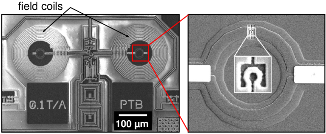
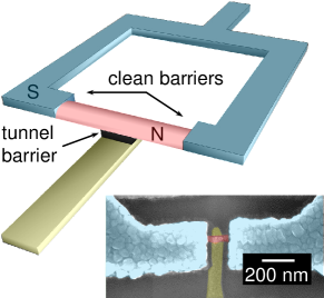
Broad-band SQUID microsusceptometers have been realized by locally modifying SQUID current sensors based on Nb/Al-AlOx/Nb JJ technology. Those sensors Drung et al. (2007) come in two types: (i) high-input inductance (H) sensors incorporate an intermediate transformer loop with gradiometric design; (ii) low-input inductance (2 nH) devices without intermediate loop; here the input signal is directly coupled to the SQUID via four single-turn gradiometric coils connected in parallel. These SQUIDs are non-hysteretic down to sub-K temperatures with at K. Modification of these sensors was done by FIB milling and FIB-induced deposition (FIBID) of superconducting material with W(CO)6 as precursor gas Martínez-Pérez et al. (2009, 2010). This allowed converting the intermediate transformer loop into a susceptometer inductively coupled to the SQUID [Fig. 4(a)]. By modifying the gradiometric microSQUID itself it is possible to directly couple an MNP to the SQUID loop Martínez-Pérez et al. (2011a) [Fig. 4(d)]. Later, SQUID-based microsusceptometers with improved reflection symmetry were produced Drung et al. (2014); Schurig (2014). The sensitivity was boosted by defining a nanoloop (450 nm inner diameter, 250 nm linewidth) by FIB milling in one of the pickup coils [Fig. 6]. These sensors offer an extremely wide bandwidth (1 mHz - 1 MHz) and can be operated at K for the investigation of microscopic crystals of SMMs and magnetic proteins; such measurements will be reviewed in section IV.3.
Submicrometric Nb/AlOx/Nb JJs in a cross-type design were recently used for fabricating miniaturized SQUIDs Schmelz et al. (2012). The key advantage of cross-type JJs over conventional window-type JJs is the elimination of the parasitic capacitance surrounding the JJ, which becomes increasingly important upon reducing the JJ size. At K, JJs show non-hysteretic IVCs, if they are shunted with a AuPd layer. Sensors are also produced with an integrated Nb modulation coil. Square-shaped washer SQUIDs with minimum inner size of m have an inductance of a few pH. SQUIDs operated in liquid He and read out with a low-noise SQUID preamplifier yield Schmelz et al. (2015).
III.2.2 Sandwich-type SNS junctions
SNS junctions (N: normal conductor) offer the advantage of large critical current densities at 4.2 K and non-hysteretic IVCs, albeit at the cost of somewhat reduced values. Hence, this type of JJs is very well suited for fabricating nanoSQUIDs with junction size in the deep submicron range.
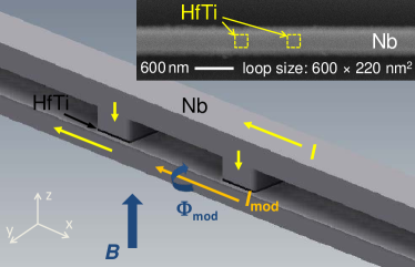
In a Nb/HfTi/Nb trilayer process, originally developed for Josephson arbitrary waveform synthesizers Hagedorn et al. (2006), JJs with area or even below are obtained by e-beam lithography and chemical-mechanical polishing, producing nanoSQUIDs Nagel et al. (2011b); Wölbing et al. (2013) with 24 nm thick HfTi barriers; the latter can be varied to modify . As for the SIS JJ technology, the fabrication process offers much flexibility for realizing complex designs. Both series- and parallel-gradiometers and single SQUID loops were realized Nagel et al. (2011b); Wölbing et al. (2013); Bechstein et al. (2015). Devices were patterned in a washer- or microstrip-type geometry, with the loop plane parallel or perpendicular to the junction’s (substrate) plane, respectively. A key advantage of the microstrip-type geometry [Fig. 7] is the possibility to realize very small loop areas, defined by the thickness of the insulating interlayer between the top an bottom Nb lines times the lateral separation of the two JJs. This results in very small SQUID inductances, typically a few pH. Moreover, a magnetic field applied in the plane of the SQUID loop can be perpendicular to the JJ (and substrate) plane; in this way the field-induced suppression of can be avoided. It has been shown that magnetic fields up to 0.5 T can be applied while degrading only marginally the performance Wölbing et al. (2013). On-chip flux biasing is easily possible for operation in FLL. White flux noise has been obtained. Based on numerical solutions of the London equations for , this yields a spin sensitivity of just for a magnetic dipole 10 nm away from the SQUID loop. Magnetization measurements on magnetic nanotubes have been performed successfully and will be summarized in section IV.2.
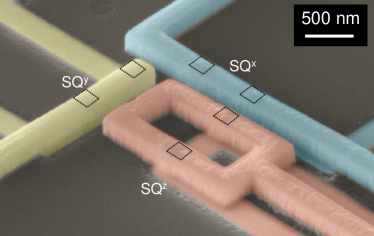
By combining three mutually orthogonal nanoSQUID loops, a 3-axis vector magnetometer has been realized very recently Martínez-Pérez et al. (2016). Here, the idea is to distinguish the three components of the vector magnetic moment of a MNP placed at a specific position, and subjected to an applied magnetic field along -direction for magnetization reversal measurements. The layout of the device is shown in Fig. 8. Two microstrip-type Nb nanoSQUIDs SQx and SQy, as described above, with perpendicular loops are sensitive to fields in - and -direction, respectively. A third SQUID, SQz has a gradiometric layout, in order to strongly reduce its sensitivity to the applied homogeneous magnetic field. Simultaneous operation of all three nanoSQUIDs in such devices in FLL has been demonstrated at 4.2 K in fields up to 50 mT, with a flux noise . By numerical simulations of the coupling factor, it has been demonstrated that for a MNP placed in the center of the left loop of the gradiometer (cf. Fig. 8), the three orthogonal components of the magnetic moment of the MNP can be detected with a relative error flux below 10 %. Such a device can provide important information on the magnetic anisotropy of a single MNP.
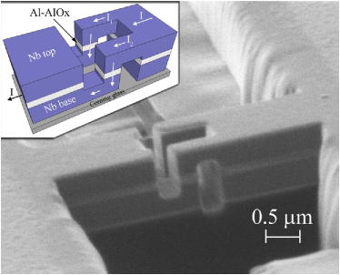
Submicrometer nanoSQUIDs have recently also been fabricated based on SNIS JJs Granata et al. (2013b). Starting from a Nb/Al-AlOx/Nb trilayer, a three dimensional SQUID loop () was nanopatterned by FIB milling and anodization [Fig. 9]. The resulting JJs have an area of approximately and are intrinsically shunted by the relatively thick (80 nm) Al layer, yielding non-hysteretic IVCs. The smallness of the SQUID loop leads to pH. Measurements at 4.2 K yield .
III.2.3 Constriction junctions
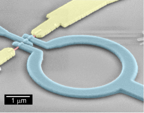
Josephson coupling can also occur in superconducting constrictions (Dayem bridges Anderson and Dayem (1964)) with size similar to or smaller than the coherence length Likharev (1979). The IVCs of such constriction-type Josephson junctions (cJJs) are often hysteretic, due to the heat dissipated above . Short enough cJJs show a sinusoidal CPR; however, a significant deviation occurs if the constriction length is larger than , which can even lead to multivalued CPRs. Hence, optimization of SQUID performance based on an RCSJ analysis is difficult, and hysteretic IVCs prevents conventional SQUID operation with current bias. Still, non-hysteretic IVCs can be achieved by operation close enough to , were is reduced, or by adding a metallic overlayer as a resistive shunt. Another drawback is the large kinetic inductance of the constriction, that can dominate the total SQUID inductance and prevent improving the flux noise by shrinking the loop size. On the other hand, cJJ-based nanoSQUIDs in a simple planar configuration can be fabricated relatively easily from thin film superconductors, e.g., Al, Nb or Pb, through one-step electron-beam (e-beam) or FIB nanopatterning. Moreover, the use of nanometric-thick films and the smallness of the constriction makes these SQUIDs quite insensitive to in-plane magnetic fields and yields large coupling factors if MNPs are placed close to the constriction [Fig.10(a)]. The small size of cJJs is a key advantage for fabricating nanoSQUIDs with high spin sensitivity.
First thin film Nb dc SQUIDs based on cJJs with linewidths down to 30 nm, patterned by e-beam lithography, were reported in 1980 Voss et al. (1980). Despite their large pH, miniaturized SQUIDs, with loop size , exhibited low flux noise at 4.2 K. During the 1990s, the use of cJJ nanoSQUIDs for the investigation of small magnetic systems was pioneered by Wernsdorfer et al.Wernsdorfer et al. (1995a); Wernsdorfer (2001, 2009). Figure 10(b) shows examples of such devices, which were patterned by e-beam lithography from Nb and Al films Hasselbach et al. (2000). Typical geometric parameters were inner loop area, 200 nm minimum linewidth and 30 nm film thickness. The size of the constrictions (nm wide, nm long) was significantly larger than for Nb. This lead to a highly non-ideal CPR Likharev (1979); Faucher et al. (2002) and hence non-ideal dependence with strongly suppressed modulation depth for Nb cJJ SQUIDs. Furthermore, of the constrictions can be a few 100 pH, dominating the overall inductance of the devices Faucher et al. (2002). Impressively large magnetic fields could be applied parallel to the nanoSQUID loops up to 0.5 T for Al and 1 T for Nb. From the measured critical current noise, the flux noise was calculated as for Al and for Nb Hasselbach et al. (2000). Due to hysteretic IVCs these nanoSQUIDs were operated in readout mode or as threshold detectors (see section II.3.3). These sensors allowed the vastest realization of true magnetization measurements (section IV.3) and were also implemented into probe tips to perform scanning SQUID microscopy Hasselbach et al. (2000); Veauvy et al. (2002).
For similar Nb cJJ-based nanoSQUIDs (30 nm thick, nm inner loop size, cJJs down to 280 nm long and 120 nm wide) switching current distributions were measured from 4.2 down to 2.8 K Granata et al. (2009). A detailed analysis of the noise performance for readout revealed a flux sensitivity of a few m, which was shown to arise from thermally induced fluctuations in the nanobridges. More recently, hysteretic nanoSQUIDs made of Al-Nb-W layers (m inner loop size; 40 nm wide, 180 nm long cJJs) could be operated with oscillating current-bias and lock-in read-out at K Hazra et al. (2013). In this configuration is considerably reduced due to the inverse proximity effect of W on Nb.
Nanometric Nb SQUIDs (50 nm thick, down to 150 nm inner hole size) were also fabricated by FIB milling to produce cJJs (80 nm wide, 150 nm long) Troeman et al. (2007). It was observed that Ga implantation depth can reach values of 30 nm, suppressing the superconducting properties of Nb. At K, devices with relatively small A showed nonhysteretic IVCs and could be operated in a conventional current-bias mode, yielding .
A possible way to approach the sinusoidal CPR of ideal point contacts is the use of variable thickness nanobridges. Here, the thicker superconducting banks can serve as phase reservoirs, while the variation in the superconducting order parameter should be confined to the thin part of the bridges Vijay et al. (2009). cJJ-based nanoSQUIDs were realized by local anodization of ultrathin (nm-thick) Nb films using a voltage-biased atomic force microscope (AFM) tip Bouchiat et al. (2001). This technique produced constrictions (nm wide and nm long) and variable thickness nanobridges by further reducing the constriction thickness down to few nm (within a nm long section). The latter exhibited twice as large as the former, indicating an improved CPR.
Vijay et al. Vijay et al. (2010) produced Al nanoSQUIDs based on cJJs (8 nm thick, 30 nm wide) with variable length (nm). The cJJs were either connected to superconducting banks of the same thickness (‘’2D devices”) or to much thicker (80 nm) banks (‘’3D devices”). For 3D devices with , the measured curves indicate a CPR which is close to the one for an ideal short metallic weak link. Both 2D and 3D devices were fully operative up to in-plane magnetic fields of 60 mT Antler et al. (2013). Such nanoSQUIDs were operated with dispersive readout (see section II.3.4) yielding impressive flux noise values of for a 20 MHz bandwidth Levenson-Falk et al. (2013).
Variable thickness bridges have recently also been realized by connecting suspended Al nanobridges (25 nm thick, 233 nm long, 60 nm wide) to Nb(30 nm)/Al(25 nm) bilayer banks to form a nanoSQUID (m-in-diameter loop)Hazra et al. (2014). These devices have the advantage of using cJJs from a material (Al) with relatively large , while maintaining relatively high and critical magnetic field in the superconducting banks forming the SQUID loop.
Thermal hysteresis in the IVCs of cJJs can be suppressed by covering the devices with a normal metallic layer, which provides resistive shunting and acts as a heat sink. cJJ-based nanoSQUIDs from 20 nm-thick Nb films covered by 25 nm-thick Au have been patterned by e-beam lithography to realize 200 nm inner loop size and constriction widths in the range nm, yielding pH Lam and Tilbrook (2003) . The Au layer prevented hysteresis in the IVCs at temperatures above 1 K, allowing conventional SQUID readout in the voltage state, yielding at 4.2 K, increasing by about 15 % when operating in a magnetic field of 2 mT Lam (2006). Field operation up to few 100 mT was improved by reducing the hole size down to 100 nm and the largest linewidths down to 250 nm Lam et al. (2011). Preliminary experiments were performed on ferritin nanoparticles attached to the cJJs Vohralik and Lam (2009). However, the magnitude of the flux change observed in some cases (up to ) was larger than the expected one for a ferritin NP located at optimum position (up to ).
Low-noise nanoSQUIDs from a Nb/amorphous W bilayer (200 and 150 nm thick, respectively) have been produced by FIB milling Hao et al. (2008). The SQUID loop (370 nm inner diameter) was intersected by two nanobridges (65 nm wide and nm long) which showed non-hysteretic IVCs at K. Readout in the voltage state gave at 6.8 K. Recently, the same group extended the operation temperatures down to K by using superconducting Ti films, inversely proximized by Au layers to reduce Blois et al. (2013). These SQUIDs (with 40 nm wide and 120 nm long constrictions) exhibited no hysteresis within mK and had . These devices allowed the detection of the magnetic signal produced by a 150 nm diameter FePt nanobead having at 8 K in fields up to 10 mT Hao et al. (2011).
As mentioned earlier, cJJ-based nanoSQUIDs can be operated in strong magnetic fields applied in the plane of the loop, which is limited by the upper critical field of the superconductors. The use of very thin superconducting layers can increase the effective critical field. Following this idea, nm-thick cJJ Nb nanoSQUIDs were fabricated, supporting in-plane fields up to 10 T. These sensors proved to be well suited for measuring magnetization curves of microcrystals of Mn12 SMMs Chen et al. (2010). However, their large kinetic inductances lead to large flux noise (). More promising is the use of materials with larger upper critical fields, such as boron-doped diamond Mandal et al. (2011). Micrometric SQUIDs based on 100 nm-wide constrictions in 300 nm thick films were demonstrated to operate up to impressive fields of 4 T applied along any direction. These devices were, however, hysteretic due to heat dissipation. Flux sensitivity was determined from the critical current uncertainty giving .
III.2.4 Proximized structures
A normal metal in good contact between superconducting electrodes acquires some of their properties due to the proximity effect, inducing a mini-gap in the density of states of the normal metal. Andreev pairs can propagate along relatively long distances at low , carrying information on the macroscopic phase of the superconductor. In the long (short)-junction regime, when the Thouless energy of the metal is larger (smaller) than the superconducting energy gap, the junction properties will be governed by the normal metal (superconductor).
The first dc SQUID built with long proximized JJs was based on a CNT intersecting an Al ring Cleuziou et al. (2006). A gate-modulated supercurrent was demonstrated and flux-induced modulation of the critical current (few nA) was observed at mK temperatures. The goal was to exploit the small cross section of the CNT () to provide optimum coupling for molecular nanomagnets attached to it. An experimental proof-of-principle of such a CNT-based magnetometer is, however, still missing. A micrometric dc SQUID with graphene proximized junctions (50 nm long, m wide) was also reported Girit et al. (2009). Flux-induced modulation was observed, however, no noise performance of the device was reported.
Micrometric dc SQUIDs containing normal metal bridges as weak links have also been reported. Nb/Au/Nb and Al/Au/Al-based devices showed IVCs with pronounced hysteresis, due to heat dissipated in the normal metal after switching Angers et al. (2008). SQUIDs with shorter Cu nanowires (nm long, nm wide, 20 nm thick) enclosed in a V ring were non-hysteretic. NanoSQUIDs based on proximized InAs nanowires (nm diameter, 20 or 50 nm long) were also reported Spathis et al. (2011) with JJs in the intermediate length regime [Fig.11].
A different kind of interferometer consists of a superconducting loop interrupted by a normal metal island. A magnetic field applied to the loop varies the phase difference across the normal metal wire, allowing flux-modulation of the minigap. This behavior can be probed by an electrode tunnel-coupled to the normal metal island [Fig.12], providing a flux-modulated electric response similar to conventional dc SQUIDs. This device received the name Superconducting Quantum Interference Proximity Transistor (SQUIPT), for being the magnetic analog to the semiconductor field-effect transistor. SQUIPTs were pioneered by Giazotto et al. Giazotto et al. (2010) using Al loops and Cu wires (m long, nm wide). These magnetometers were further improved by reducing the length of the normal metal island down to the short-junction limit, leading to a much larger mini-gap opening. By choosing proper dimensions of the normal metal island, such sensors do not exhibit any hysteresis down to mK temperatures Jabdaraghi et al. (2014); Ronzani et al. (2014) and can be voltage or current biased, providing impressive values of of a few mV/. SQUIPTs are in their early stage of developmentAlidoust et al. (2013), still showing a very narrow temperature range of operation limited to sub-kelvin. On the other hand, they exhibit record low dissipation power of just fW (pA, mV) and should achieve flux noise levels of just a few n. The latter has not been determined experimentally yet due to limitations from the voltage noise of the room temperature amplifiers.
III.3 NanoSQUIDs based on cuprate superconductors
High- cuprate superconductors such as YBCO have very small and anisotropic values of , reaching nm for the plane and a minute nm for the axis, making the fabrication of cJJs extremely challenging. Still, the fabrication of YBCO cJJs with nm cross-section and nm length has been reported recently Arpaia et al. (2014). These JJs exhibit large of a few mA at 300 mK. NanoSQUIDs based on this technology were fabricated and preliminary measurements showed low flux noise at 8 K.
Probably the most mature JJs from cuprate superconductors are based on Josephson coupling across grain boundaries (GBs). Grain boundary junctions (GBJs) can be fabricated, e.g., by epitaxial growth of cuprate superconductors on bicrystal substrates or biepitaxial seed layers Hilgenkamp and Mannhart (2002); Tafuri and Kirtley (2005); Tafuri et al. (2013). Although micrometric SQUIDs based on GBJs have been produced Koelle et al. (1999), the miniaturization of high-quality GBJs is challenging, because of degradation of the material due to oxygen loss during nanopatterning. NanoSQUIDs made of high- GBJs are, on the other hand, very attractive due to their large critical current densities ( at 4.2 K) and huge upper critical fields (several tens of T).
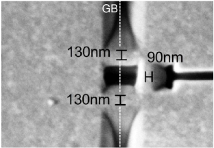
YBCO GBJ nanoSQUIDs were fabricated by FIB milling Nagel et al. (2011a); Schwarz et al. (2013, 2015). Devices consist of nm thick YBCO epitaxially grown on bicrystal SrTiO3 substrates ( misorientation angle) and covered by typically 60 nm thick Au serving as resistive shunt and to protect the YBCO during FIB milling. Typical inner hole size is nm and GBJs are nm wide [Fig. 13]. Devices are non-hysteretic and work from K up to K. Large magnetic fields can be applied perpendicular to the GBJs in the substrate plane, without severe degradation of the modulation for fields up to 3 T Schwarz et al. (2013). Via a modulation current through a constriction (down to nm wide) in the loop, the devices can be flux-biased at their optimum working point, without exceeding the critical current, i.e. the constriction is not acting as a weak link. The constriction is also the position of optimum coupling of a MNP to the SQUID.
Numerical simulations based on London equations for variable SQUID geometry provided expressions for and [via Eq. (10)] for a magnetic dipole 10 nm above the constriction, as a function of all relevant geometric parameters. Together with RCSJ model predictions for at 4.2 K, an optimization study for the spin sensitivity has been performed. An optimum film thickness nm was found (for nm). For smaller , the increasing contribution of to the flux noise dominates over the improvement in coupling. For optimum and , the spin sensitivity decreases monotonically with decreasing constriction length (which fixes the optimum constriction width ). For and of several tens of nm, an optimum spin sensitivity of a few was predicted in the white noise limit Wölbing et al. (2014).
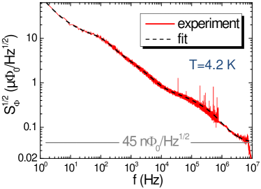
For an optimized device with small inductance pH (nm, nm, nm), direct readout measurements of the magnetic flux noise at 4.2 K gave at 7 MHz (close to the intrinsic thermal noise floor), which is amongst the lowest values reported for dc SQUIDs so far [Fig. 14]. With a calculated coupling factor , this device yields a spin sensitivity of at 7 MHz and 4.2 K Schwarz et al. (2015). Due to the extremely low white noise level, -like excess noise dominates the noise spectrum within the entire bandwidth of the readout electronics. Bias reversal can only partially eliminate this excess noise, which deserves further investigation.
Finally, an encouraging step towards the controlled formation and further miniaturization of high- JJs has been made recently by Cybart et al. (2015). For this purpose a 0.5-nm-diameter He+-beam was used to fabricate nm-narrow ion-irradiated barriers on m wide and 30 nm thick YBCO bridges. The key point is the smallness of the ion beam diameter, which allows the introduction of point like defects. By varying the irradiation dose between the authors showed the successful realization of JJs exhibiting SNS-like or tunnel-like behavior. This technique has been applied to the fabrication of SQUID devices Cho et al. (2015), but their downsizing to the nanoscale still needs to be realized.
IV nanoSQUIDs for magnetic particle detection
Originally, nanoSQUIDs were conceived for the investigation of individual MNPs and SMMs. These systems are of key technological importance with applications ranging from electronics, including hard discs, magnetic random access memories, giant magneto resistance devices, and spin valves, through on-chip adiabatic magnetic coolers, and up to biotechnology applications including enhanced imaging of tissues and organs, virus-detecting magnetic resonance imaging, and cancer therapy (see, e.g., Ref. MRS (2013)). Moreover, magnetic molecules appear as an attractive playground to study quantum phenomena Bartolomé et al. (2014) and could eventually find application in emerging fields of quantum science such as solid-state quantum information technologies Leuenberger and Loss (2001) and molecular spintronics Bogani and Wernsdorfer (2008).
In this section we will review, as an important application of nanoSQUIDs, the investigation of small magnetic particles. We will first address challenges and approaches regarding positioning of MNPs close to the SQUIDs and then discuss measurements of magnetization reversal and of ac susceptibility of MNPs.
IV.1 Nanoparticle positioning
The manipulation and positioning of MNPs close to the nanoSQUIDs is particularly important since the magnetic signal coupled to any form of magnetometer strongly depends on the particle location with respect to the sensor. Although conceptually very simple, this problem has hampered the realization of true single-particle magnetic measurements so far. Many strategies have been developed to improve the control on the positioning of MNPs or SMMs on specific areas of nanoSQUID sensors.
IV.1.1 In-situ nanoparticle growth
In an early approach, called the drop-casting method, small droplets with suspended MNPs were deposited on a substrate containing many nanoSQUIDs. After solvent evaporation some of the MNPs happened to occupy positions of maximum coupling. This method was successfully applied to investigate nm individual Co MNPs Wernsdorfer et al. (1997a) . In a similar approach, MNPs based on Co, Fe or Ni were sputtered using low-energy cluster beam deposition techniques onto substrates containing a large amount of microSQUIDs Wernsdorfer et al. (1995b). Alternatively, MNP and Nb deposition was realized simultaneously to embed nanometric clusters into the superconducting films, which were subsequently patterned to form nano- or microSQUIDs Jamet et al. (2000). The drawback of these techniques is the lack of precise control of the MNP positions relative to the SQUIDs, which requires the use and characterization of many tens or even hundreds of SQUIDs.
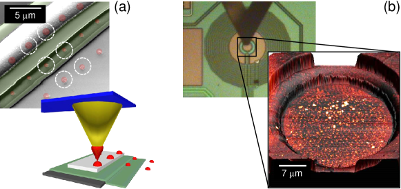
Improved nanometric control over the particle position can be achieved by nanolithography methods. This has been used to define Co, Ni, TbFe3 and Co81Zr9Mo8Ni2 MNPs with smallest dimension of Wernsdorfer et al. (1995a). Alternatively, focused e-beam induced deposition (FEBID) of high-purity cobalt (from a precursor gas, e.g., Co2(CO)8 Córdoba et al. (2010)) allows the definition of much smaller particles (down to nm) and arbitrary shape located at precise positions with nanometric resolution. This technique has been successfully applied to the integration of amorphous Co nanodots onto YBCO nanoSQUIDs [Fig. 15(a)]Martínez-Pérez et al. (2017).
IV.1.2 Scanning probe-based techniques
The use of a scanning probe, e.g., the tip of an AFM can be used for precise manipulation of the position of a MNP. AFM imaging in non-contact mode is first used to locate MNPs dispersed over a surface Then, using contact mode, the tip is used to literally ‘’push” the MNP to the desired position Martin et al. (1998); Pakes et al. (2004). This technique was applied to improve the coupling between a nanoSQUID and Fe3O4 NPs (15 nm diameter) deposited via the drop-casting method Wernsdorfer (2009). Micro- and nanomanipulators installed inside SEMs have also been used for this purpose. For instance, a sharpened carbon fiber mounted on a micromanipulator in a SEM has been used to pick up a m diameter single FePt particle an deposit it onto a nanoSQUID Hao et al. (2011).
Alternatively, larger carriers that are more easily visible and manipulated can be used to manipulate the position of MNPs. For example, microscopic SiNi cantilevers containing the MNP of interest can be moved using a micromanipulator Gella (2015) [Fig. 15(b)]. In particular, CNTs appear as promising tools for this purpose. SMMs have indeed been successfully grafted over or encapsulated inside CNTs, which were later used to infer their magnetic properties Ganzhorn et al. (2013). Similarly, an Fe nanowire encapsulated in a CNT has been mounted by micromanipulators on top of YBCO nanoSQUIDs for magnetization reversal measurements (see section IV.2) Schwarz et al. (2015).
Another promising approach is dip pen nanolithography (DPN). Here, an AFM tip is first coated with a solution containg MNPs and then brought into contact with a surface at the desired location. Capillarity transport of the MNPs from the tip to the surface via a water meniscus enables the successful deposition of small collections of molecules in submicrometer dimensions Piner et al. (1999). Bellido et al. Bellido et al. (2010) showed that this technique can be applied to the deposition of dot-like features containing monolayer arrangements of ferritin-based molecules onto microSQUID sensors [Fig. 16(a)] for magnetic susceptibility measurements Martínez-Pérez et al. (2011b) (section IV.3). The number of MNPs deposited per dot can be controlled (via the concentration of the ferritin solution and dot size) from several hundred of proteins down to individual ones Bellido et al. (2010). Recently, DPN has also been applied to the deposition of dot-like features containing just molecular layers of Mn12 and Dy2 SMMs onto the active areas of microSQUID-based susceptometers, enabling the detection of their magnetic susceptibility Bellido et al. (2013); Jenkins et al. (2015) [Fig. 16(b)].
Recently, individual magnetic nanotubes, attached to an ultrasoft cantilever were brought in close vicinity to a nanoSQUID at low Buchter et al. (2013); Nagel et al. (2013); Buchter et al. (2015). This technique allowed the authors to investigate magnetization reversal of the nanotubes by combining torque and SQUID magnetometry (see section IV.2).
We note that scanning SQUID microscopy could also be applied to the study of MNPs deposited randomly on surfaces Kirtley (2009). This would provide an elegant way of locating magnetic systems close enough to the sensor and would also enable in-situ reference measurements. However, their use for the investigation of magnetic molecules or nanoparticles arranged on surfaces is still awaiting.
IV.1.3 Techniques based on chemical functionalization
The above mentioned techniques can be further improved by chemically functionalizing the sensor’s surface or the MNPs or both of them Bellido et al. (2012). This usually provides high quality monolayers or even individual magnetic molecules at specific positions. For instance, Mn12 SMMs could be successfully grafted on Au, the preferred substrate for chemical binding, by introducing thiol groups in the clusters Cornia et al. (2003). In a further step, such Mn12 molecules could be individually isolated by a combination of molecule and Au substrate functionalization Coronado et al. (2005).
This technique has also been applied to the deposition of ferritin-based MNPs onto Au-shunted nanoSQUIDs Lam et al. (2008). For this purpose, a window was opened through e-beam lithography onto a PMMA layer deposited on top of the nanoSQUID. This window was then covered with organic linkers that were later used to attach the ferritin MNPs. The success of this process was finally determined by AFM, showing evidence that few proteins were attached.
IV.2 Magnetization measurements
NanoSQUIDs can be applied to study the reversal of magnetization of MNPs placed nearby. For this purpose an external magnetic field is swept while recording changes in the magnetic moment of the sample coupled as a change of magnetic flux to the SQUID [Fig. 4(b)]. Usually, is hysteretic, due to an energy barrier created by magnetic anisotropy. Such hysteresis loops reveal information on the reversal mechanisms, e.g. domain wall nucleation and propagation or the formation of topological magnetic states like vortices, coherent rotation, or quantum tunneling of magnetization. Depending on the particle’s anisotropy, this requires the application of relatively large , a difficult task when dealing with superconducting materials. Measurements are usually done by careful alignment of with respect to the nanoSQUID, to minimize the magnetic flux coupled to the loop and the JJs by directly. The maximum will be limited by the upper critical field of the superconducting material, e.g. T for Nb films, unless ultrathin films are used, which however increases significantly and hence the flux noise (see section III.2.3).
The vastest amount of dc magnetization studies performed on individual MNPs was provided by the pioneering work of Wernsdorfer and co-workers. They were able to measure magnetization curves of a number of MNPs made of Ni, Co, TbFe3 and Co81Zr9Mo8Ni2 with sizes down to . Furthermore, they succeeded in measuring the dc magnetization of the smallest MNPs ever detected to date. These are 3 nm diameter crystalline Co MNPs ( each) directly embedded into the Nb film forming the nanoSQUID Jamet et al. (2001). The detected magnetization switching process was attributed to an individual MNP located precisely at the cJJ, where the coupling factor is maximized. These studies also enabled the determination of the and order anisotropy terms in the magnetic anisotropy of the Co MNPs. Additionally, many exciting phenomena were studied with this technique. These include, e.g., the observation of Stoner-Wohlfarth and Néel-Brown type of thermally assisted magnetization reversal in individual Co clusters (25 nm, ) Wernsdorfer et al. (1997a) or the observation of macroscopic quantum tunneling of magnetization in BaFeCoTiO single particles (nm, ) Wernsdorfer et al. (1997b). Magnetization reversal triggered by rf field pulses on a 20 nm diameter Co NP was also reported Thirion et al. (2003) and, recently, the effects of the antiferromagnetic-ferromagnetic exchange bias between a Co nanocluster and a CoO layer were revealed Le Roy et al. (2011). Micrometric SMM crystals were also investigated with an array containing four microSQUIDs Wernsdorfer (1996). These experiments allowed observing the modulation of the small (K) tunnel splitting in Fe8 molecular clusters under the application of a transverse magnetic field Wernsdorfer and Sessoli (1999).
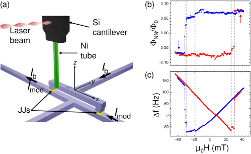
Magnetization reversal mechanisms in single Ni and permalloy nanotubes were investigated using Nb/HfTi/Nb-based nanoSQUIDs Buchter et al. (2013); Nagel et al. (2013); Buchter et al. (2015). Experiments were performed at 4.2 K with applied along the nanotube axis (-axis), with the SQUID loop in the - plane. The nanoSQUID was mounted on an -- stage below the bottom end of the nanotube which is affixed to an ultrasoft Si cantilever [Fig.17(a)]. The nanotube was positioned to maximize the flux coupled to the nanoSQUID. While recording the SQUID output operated in FLL, simultaneously the magnetic torque exerted on the nanotube was detected, by recording the frequency shift on the cantilever resonance frequency as a function of . Measurements on a Ni nanotube showed discontinuities at the same values of that were ascribed to switching of the magnetization along the nanotube [Fig. 17(b)]. These experiments provided, on the one hand, the magnetic field stray produced by the nanotube’s end and, on the other, the volume magnetization, giving evidence for the formation of a magnetic vortex-like configuration in the nanotube. Measurements on an individual permalloy nanotube evidenced the nucleation of magnetic vortices at the nanotube’s end before propagating through its whole length, leading to the complete switching of the magnetization. Furthermore, it has been shown that a thin exchange-coupled antiferromagnetic native-oxide layer on the nanotube modifies the magnetization reversal process at low temperatures Buchter et al. (2015).
YBCO nanoSQUIDs were used for the investigation of magnetization reversal in a Fe nanowire grown inside a CNT attached on top of the SQUID Schwarz et al. (2015) [Fig.18(a)]. Magnetization measurements were performed at 4.2 K in FLL by continuously sweeping in the plane of the SQUID loop, along the Fe wire axis. Rectangular shaped hysteresis loops [Fig.18(b)] indicate a single domain state for the nanowire. The magnitude of the switching field suggests that magnetization reversal takes place non-uniformly, e.g., by curling. These results agree very well with previous measurements on an individual nanowire using a micro-Hall bar Lipert et al. (2010), albeit with a significantly improved signal-to-noise ratio. Similarly, YBCO nanoSQUIDs were used to detect the magnetization reversal of individual Co MNPs with magnetic moments at different temperatures ranging from 300 mK up to 80 K. These studies allowed the identification of two different reversal mechanisms which depend on the dimensions and shape of the Co particles. The different reversal mechanisms are linked to the stabilization two different magnetic states, i.e., the (quasi) single-domain and the vortex state Martínez-Pérez et al. (2017).
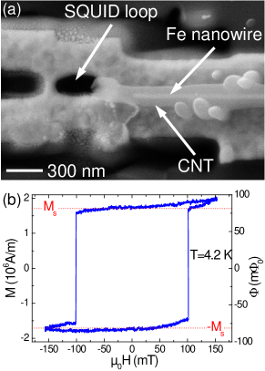
(a) SEM image of Fe nanowire encapsulated in a CNT on top of a YBCO nanoSQUID. (b) Hysteresis loop of the Fe nanowire, detected by the SQUID. Left axis corresponds to magnetization signal ; the literature value for the saturation magnetization kA/m of Fe is indicated as dashed lines. [after Schwarz et al.Schwarz et al. (2015)]
IV.3 Susceptibility measurements
Even more demanding, nanoSQUIDs can also be used to quantify the response of a MNP to an oscillating magnetic field , i.e., its frequency-dependent magnetic susceptibility , where is the part going in-phase with and is the out-of-phase part. These quantities bear much information on the dynamic behavior of spins and the relaxation processes to thermal equilibrium, the interaction between spins, and the ensuing magnetic phase transitions. These measurements can be performed using SQUID-based susceptometers, usually in a gradiometric design to be insensitive to homogeneous external magnetic fields, but sensitive to the imbalance produced by a MNP located in one of the coils [Fig. 4(c,d)]. and are directly accessible by applying a homogeneous via on-chip excitation coils and lock-in detecting the nanoSQUID output. Alternatively, can be measured, as it is directly related to through the fluctuation-dissipation theorem Reim et al. (1986). The detection of demands high sensitivity, as the net oscillating polarization induced in the sample is, by far, smaller than the total saturation magnetization. At best, broad-band frequency measurements must be performed which also provide an easy way to filter out the noise of the SQUIDs, therefore improving the effective sensitivity of the sensor. Frequencies are usually restricted to MHz, mainly limited by the room temperature amplifiers and the FLL circuit.
One of the most controversial observations of quantum coherence in nanoscopic magnets was realized using the SQUID-based microsusceptometer developed by Ketchen et al. Ketchen et al. (1984). This device allowed the detection of the magnetic susceptibility of small spin populations of natural horse-spleen ferritin Awschalom et al. (1992a). For a sample with just proteins (/protein), a resonance peak in both the out-of-phase component of and has been observed and was attributed to the zero-field splitting energy Awschalom et al. (1992a, b). This is the energy separating the two non-degenerated low-energy quantum states, i.e., the (anti-)symmetric combination of the classical states corresponding to magnetization pointing (down) up. This interpretation and the magnitude of this zero-field splitting (900 kHz) is still an object of debate.
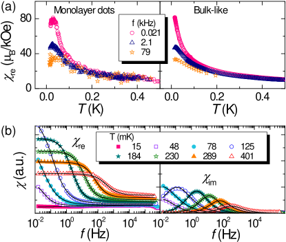
MNPs artificially grown inside ferritin were also studied using a SQUID-based microsusceptometer Martínez-Pérez et al. (2011b). The magnetic core with diameter of just a few nm was composed of antiferromagnetic CoO leading to a tiny magnetic moment of per protein. Monolayer arrangements of ferritin MNPs (total amount proteins) were deposited by DPN directly onto the SQUID, maximizing the coupling between the samples and the sensor’s pickup coils Bellido et al. (2010) (see section IV.1.2). Using mT, these experiments showed that ferritin-based MNPs arranged on surfaces retain their properties, still exhibiting superparamagnetic blocking of the magnetic susceptibility [Fig. 19(a)]. Furthermore, these results allowed to determine experimentally the spin sensitivity. This was done by determining the coupling, i.e., the measured flux signal coupled to the microsusceptometer divided by the total magnetic moment of the particle, which was located at an optimum position on top of the field coil or close to the edge of the pickup-loop. Together with the measured flux noise of the SQUID, this yielded . Additionally, a large amount of measurements on SMM micron-sized crystals or powder at very low were reported [Fig. 19(b)]. The large bandwidth of these susceptometers (1 mHz–1 MHz) enabled, e.g., the investigation of the relationship between quantum tunneling and spin-phonon interaction and to point out novel and reliable molecular candidates for quantum computing and low-temperature magnetic refrigerants (e.g., Refs. Luis et al. (2011); Martínez-Pérez et al. (2011a, 2012a, 2012b)).
Microsusceptometers were also used to detect the ac magnetic susceptibility of just Mn12 SMMs arranged as dot-like features containing 3–5 molecular layers Bellido et al. (2013). Measurements showed an evident decrease of the magnetic relaxation time compared to that observed in crystalline Mn12. This phenomenon was attributed to structural modifications of the surface-arranged molecules leading to an effective decrease of their activation energy. These sensors have been also applied to the investigation of quantum spin dynamics of Fe4 SMMs grafted onto graphene flakes Cervetti et al. (2016).
V nanoSQUIDs for scanning SQUID microscopy
In scanning SQUID microscopy (SSM) the high sensitivity of SQUIDs to magnetic flux is combined with high spatial resolution by scanning a sample under investigation relative to a miniaturized SQUID sensor, or vice versa. A variety of SSM systems has been developed in the 1990s and refined since then. Those were based on both, metallic low- and high- cuprate superconductors, although the majority of work focused on the low- devices. For a review on the developments of SSM in the 1990s see Ref. Kirtley (2002).
Obviously, miniaturized SQUID structures can significantly improve the spatial resolution and sensitivity to local magnetic field sources. A key issue is the requirement to approach the surface of the samples under investigation to a distance which is of the order of or even smaller than the SQUID size or pickup loop, in order to gain in spatial resolution by shrinking the lateral dimensions of the structures. Several strategies for improving the spatial resolution in SSM have been followed, which can be divided into three approaches. The two conventional approaches, developed in the 1990s use SQUID structures on planar substrates. One is based on the sensing of local fields by a miniaturized pickup loop, coupled to a SQUID sensor; the other is based on using miniaturized SQUID loops to which local magnetic signals are coupled directly (section V.1). A very recently developed third approach uses the SQUID-on-tip (SOT), i.e. a SQUID deposited directly on top of a nanotip (section V.2).
V.1 SQUID microscopes using devices on planar substrates
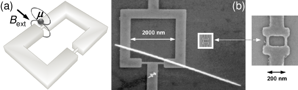
SQUID microscopes developed at IMB research by Kirtley et al. Kirtley et al. (1995) are based on Nb/Al-AlOx/Nb technology. The sensors are based on a single SQUID loop with an integrated pickup loop Ketchen et al. (1989). The pickup loops have diameters down to m and are connected via well shielded superconducting thin film leads to the SQUID loop at typically mm distance on the same chip Ketchen and Kirtley (1995). This technology has also been used to realize a miniature vector magnetometer for SSM by using three SQUIDs with orthogonal pickup loops on a single chip Ketchen et al. (1997). As a key advantage, the IBM designs are based on the very mature Nb multilayer SIS technology, including patterning by photolithography, that allows e.g. using the HYPRES 555www.hypres.com process for sensor fabrication. Moreover, this allows to integrate field coils around the pickup loop for susceptibility measurements and modulation coils inductively coupled to the SQUID loop for separate flux modulation of the SQUID, i.e. without disturbing the signals to be detected by the pickup loop. The Si substrate is polished to form a corner, typically at a distance of a few tens of m away from the center of the pickup loop. SQUID microscopes based on such sensors use a mechanical lever for scanning. The SQUID chip is mounted on a cantilever with a small inclination angle to the plane of the sample. The vertical pickup-loop to sample distance is then given by Kirtley et al. (1995). If the SQUID is well thermally linked to the liquid He bath for operation at 4.2 K, the sample mounted in vacuum can be heated to above K Kirtley et al. (1999).
The most important application of the IBM microscope was the pioneering work on the order parameter symmetry of cuprate superconductors. Just to mention a few examples, this includes key experiments for providing clear evidence of -wave pairing in the cuprates by imaging fractional vortices along YBCO GBJs Mannhart et al. (1996), the formation of half-integer flux quanta in cuprate tricrystals Tsuei et al. (1994) and in Nb/cuprate hybrid Josephson junctions, forming zigzag-type JJs or huge arrays of -rings Hilgenkamp et al. (2003). For more applications, see the review Kirtley (2010).
Very similar devices, also based on the Nb multilayer technology, have been developed and used for SSM by the Stanford group of Moler and co-workers Gardner et al. (2001); Huber et al. (2008). Based on the original microsusceptometer design of Ketchen et al. Ketchen et al. (1989), these devices contain two oppositely wound pickup coils, to cancel homogeneous applied fields. Sensors with m pickup-loop diameter achieved at 4 K and below 0.5 K Huber et al. (2008); Koshnick et al. (2008). The sensor’s substrate was cut by polishing, leading to . A capacitive approach control was used to monitor the probe-to-sample distance. These microsusceptometers were largely improved by using a terraced cantilever obtained through a multilayer lithography process. In this way the pickup loop stands above the rest of the structure lying at just 300 nm above the sample surface. Additionally the pickup loop diameters were reduced down to 600 nm using focused ion beam (FIB) milling Koshnick et al. (2008). Based on these SQUID sensors, the Stanford group has developed a SQUID microscope operating at temperatures down to 20 mK in a dilution refrigeratorBjörnsson et al. (2001).
The SSM system of the Stanford group has been very successfully applied to a variety of interesting systems. Just to give a few examples, this includes the study of edge currents in topological insulators Nowack et al. (2013), surface magnetic states Bert et al. (2011) and twin walls Kalisky et al. (2013) at the LaAlO3/SrTiO3 interface, or unpaired spins in metals Bluhm et al. (2009).
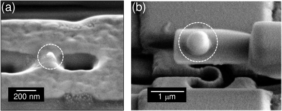
As an alternative approach, the group of Hasselbach and co-workers at Institut Néel, Grenoble developed an SSM based on miniaturized Nb and Al SQUIDs loops with constriction JJs Hasselbach et al. (2000), very similar to the ones of the Wernsdorfer group Wernsdorfer (2009). This approach allows for a relatively simple single layer fabrication process with prospects of strong miniaturization. To achieve at the same time small probe-to-sample distances, the sensor’s substrate was cut using a dicing machine and a mesa was defined by means of reactive ion etching so that the distance between the SQUID and apex of the mesa (‘tip’) was only m. With an inclination angle , this gives a smallest vertical distance to a sample surface of m. The SSM setup is combined with force microscopy, based on the use of a mechanically excited quartz tuning fork and operates in a dilution refrigerator, achieving minimum SQUID and sample temperatures of 0.45 K Veauvy et al. (2002). Very recently, in a modified setup, a SQUID-to-sample distance of 420 nm has been demonstrated, in a setup with 40 mK base temperature Hykel et al. (2014).
The SSM system of the Grenoble group has been applied to the investigation of basic properties of superconductors. This includes, e.g., studies on the direct observation of the localized superconducting state around holes in perforated Al films Veauvy et al. (2004) or on the Meissner-Ochsenfeld effect and absence of the Meissner state in the ferromagnetic superconductor UCoGe Paulsen et al. (2012).
V.2 SQUID-on-tip (SOT) microscope
An important breakthrough in the field of nanoSQUIDs applied to SSM was achieved recently with the implementation of the SQUID-on-tip (SOT) by the Zeldov group at the Weizman Institute of Science Finkler et al. (2010); Vasyukov et al. (2013). This device is based on the deposition of a nanoSQUID directly on the apex of a sharp quartz pipette [Fig.20]. The fact that the nanoSQUID is located on a sharp tip reduces the possible minimum probe-to-sample distances to below 100 nm, boosting enormously the spatial resolution of the microscope. Al, Nb and Pb nanoSQUIDs based on Dayem bridges are shadow-evaporated in a three-angle process, without requiring any lithography or milling steps. For this purpose, a quartz pipette is first pulled to form a sharp hollow tip with nm inner diameter. By means of a laser diode parallel to the tip, the latter is aligned pointing down towards the source which defines the position. Then a thin layer (nm) of superconducting material is deposited, followed by two thicker leads (nm) deposited at . The resulting weak links formed at the tip apex between these two leads constitute two Dayem bridges. Special care must be taken for fabricating the Nb and Pb sensors. The former require the previous deposition of a thin AlOx buffer layer to prevent contamination from the quartz tip. A dedicated ultra-high vacuum e-beam evaporation system was used for depositing Nb from a point source. On the other hand, the so far most sensitive Pb sensors require the use of a He cooling system for the tips during deposition to prevent the formation of islands due to the large surface mobility of these atoms at higher temperatures. This procedure lead to the smallest nanoSQUIDs fabricated so far, with effective nanoloop diameters down to 50 nm. The resulting inductance of the loop reaches values below 10 pH, dominated by the kinetic inductance of the thin superconducting layer. Although these nanoSQUIDs exhibit hysteretic IVCs, operation with voltage bias and reading out the resulting current signal with an SSA enables the detection of the intrinsic flux noise of the devices. The SOTs can be operated in large magnetic fields up to T (limited by the upper critical fields of the superconducting materials). So far, flux biasing to maintain the optimum working point during continuous external field sweep is not possible. By adjusting the external magnetic field to values which yield large transfer functions, these devices exhibit extraordinary low flux noise levels down to for the Pb SOTs Vasyukov et al. (2013). The latter varies, depending on the biasing external magnetic field. For a magnetic dipole located at the center of the loop with orientation perpendicular to the loop plane (assuming an infinitely narrow width of the loop, i.e. the approximation used by Ketchen et al. Ketchen et al. (1989)), this translates into a spin sensitivity of , i.e. the best spin sensitivity reported so far for a nanoSQUID.
A device able of distinguishing in-plane and out-of-plane magnetic signals was also reported Anahory et al. (2014). This is achieved by using a pipette with -shaped cross section to form a three JJ SQUID (3JSOT). This tip is later milled by FIB leading to a V shaped apex with two oblique nanoloops connected in parallel. By measuring the dependence of the maximum critical current on the externally applied in-plane and out-of-plane magnetic fields ), it is possible to determine all the geometrical and electric parameters of the device. Field components can be decoupled by biasing the 3JSOT at specific fields () in which depends strongly on one of the two orthogonal components of the magnetic field while being insensitive to the other. As a drawback, this device is not able of distinguishing both in-plane and out-of-plane components of the magnetic flux simultaneously, but only when operated at different flux biasing points.
For SSM, a system operating in a 3He system with 300 mK base temperature has been developed, with the SOT glued on a quartz tuning fork, to operate the system also in an magnetic force microscopy mode. This allows scanning (using piezo-scanners) at extremely small tip-to-sample distances of only a few nm Finkler et al. (2012). A spatial resolution below 120 nm was demonstrated by imaging vortices in Nb thin films with a 117 nm-diameter Pb SOT Vasyukov et al. (2013).
The SOT-SSM system has been successfully applied to the study of vortex trajectories in superconducting thin films, allowing the investigation of the influence of the pining force landscape Embon et al. (2015). More recently, this tool was used to observe nanoscopic magnetic structures such as ferromagnetic metallic nanoislands at the LaMnO3/SrTiO3 interface Anahory et al. (2016) or magnetic nanodomains in magnetic topological insulators Lachman et al. (2015).
VI Summary and outlook
Significant progress in thin film fabrication and pattering technologies has enabled the development of strongly miniaturized dc SQUIDs with loop sizes on the micrometer scale (microSQUIDs) or even with sub-micrometer dimensions (nanoSQUIDs), or SQUIDs coupled to miniaturized pickup loops. Such devices are based on a variety of Josephson junctions, intersecting the SQUID loop, many of them also on the sub-micrometer scale. As a key advantage of such strongly miniaturized SQUID structures, they can offer significantly reduced flux noise, down to the level of a few tens of n, corresponding to spin sensitivities around and improved spatial resolution for scanning SQUID microscopy. Hence, strongly miniaturized SQUIDs are very promising detectors for investigating tiny and strongly localized magnetic signals produced, e.g., by magnetic nanoparticles or for high-resolution scanning SQUID microscopy. Very recent advances, including the demonstration of single spin sensitivity and a breakthrough in spatial resolution of scanning SQUID microscopy open up promising perspectives for applications in nanoscale magnetism of condensed matter systems.
Acknowledgements.
We gratefully acknowledge valuable contributions by the nanoSQUID team at Tübingen, M. Kemmler, J. Nagel, R. Wölbing, T. Schwarz, B. Müller, S. Hess and R. Kleiner, and by our collaborators O. Kieler and A. Zorin et al. at PTB Braunschweig, T. Schurig et al. at PTB Berlin, B. Büchner et al. at IFW Dresden, M. Poggio et al. at Univ. Basel, D. Grundler et al. at TU Munich and EPFL Lausanne, A. Fontcuberta i Morral at EPFL Lausanne and J. Sesé at INA Zaragoza. This work was funded by the Alexander von Humboldt Foundation, the Nachwuchswissenschaftlerprogramm of the Univ. Tübingen, the Deutsche Forschungsgemeinschaft, via projects KO 1303/13-1 and SFB/TRR21, and by the EU-FP6-COST Action MP1201.References
- Clarke and Braginski (2004) J. Clarke and A. I. Braginski, eds., The SQUID Handbook, Vol. I: Fundamentals and Technology of SQUIDs and SQUID systems (Wiley-VCH, Weinheim, 2004).
- Kleiner et al. (2004) R. Kleiner, D. Koelle, F. Ludwig, and J. Clarke, “Superconducting QUantum interference devices: State-of-the-art and applications,” Proc. IEEE 92, 1534–1548 (2004).
- Clarke and Braginski (2006) J. Clarke and A. I. Braginski, eds., The SQUID Handbook, Vol. II: Applications of SQUIDs and SQUID Systems (Wiley-VCH, Weinheim, 2006).
- Gurvitch et al. (1983) M. Gurvitch, M. A. Washington, and H. A. Huggins, “High quality refractory Josephson tunnel junctions utilizing thin aluminum layers,” Appl. Phys. Lett. 42, 472–474 (1983).
- Voss et al. (1980) Richard F. Voss, Robert B. Laibowitz, and Alec N. Broers, “Niobium nanobridge dc SQUID,” Appl. Phys. Lett. 37, 656–658 (1980).
- Broers et al. (1976) A. N. Broers, W. W. Molzen, J. J. Cuomo, and N. D. Wittels, “Electron-beam fabrication of 80 Å metal structures,” Appl. Phys. Lett. 29, 596–598 (1976).
- Tesche and Clarke (1977) C. D. Tesche and J. Clarke, “DC SQUID: Noise and optimization,” J. Low Temp. Phys. 29, 301–331 (1977).
- Koch et al. (1981) Roger H. Koch, D. J. Van Harlingen, and John Clarke, “Quantum noise theory for the dc SQUID,” Appl. Phys. Lett 38, 380–382 (1981).
- Ketchen et al. (1984) M. B. Ketchen, T. Kopley, and H. Ling, “Miniature SQUID susceptometer,” Appl. Phys. Lett. 44, 1008–1010 (1984).
- Rogers (1983) F. P. Rogers, A device for experimental observation of flux vortices trapped in superconducting thin films, Ph.D. thesis, MIT, Cambridge, MA (1983).
- Wernsdorfer et al. (1995a) W. Wernsdorfer, K. Hasselbach, D. Mailly, B. Barbara, A. Benoit, L. Thomas, and G. Suran, “DC-SQUID magnetization measurements of single magnetic particles,” J. Magn. Magn. Mat. 145, 33–39 (1995a).
- Wernsdorfer (2001) W. Wernsdorfer, “Classical and quantum magnetization reversal studied in nanometersized particles and clusters,” Adv. Chem. Phys. 118, 99–190 (2001), arXiv:cond-mat/0101104v1 .
- Kirtley (2010) J. R. Kirtley, “Fundamental studies of superconductors using scanning magnetic imaging,” Rep. Prog. Phys. 73, 126501 (2010).
- Granata and Vettoliere (2016) C. Granata and A. Vettoliere, “Nano superconducting quantum interference device: A powerful tool for nanoscale investigations,” Phys. Rep. 614, 1–69 (2016), arXiv:1505.06887 [cond-mat.supr-con] .
- Schäfer-Nolte et al. (2014) Eike Schäfer-Nolte, Lukas Schlipf, Markus Ternes, Friedemann Reinhard, Klaus Kern, and Jörg Wrachtrup, “Tracking temperature-dependent relaxation times of ferritin nanomagnets with a wideband quantum spectrometer,” Phys. Rev. Lett. 113, 217204 (2014).
- Thiel et al. (2016) L. Thiel, D. Rohner, M. Ganzhorn, P.Appel, E. Neu, B. Müller, R. Kleiner, D. Koelle, and P. Maletinsky, “Quantitative nanoscale vortex imaging using a cryogenic quantum magnetometer,” Nature Nanotechnology (2016), 10.1038/nnano.2016.63, dOI: 10.1038/nnano.2016.63, arXiv:1511.02873 [cond-mat.mes-hall] .
- Ganzhorn et al. (2013) Marc Ganzhorn, Svetlana Klyatskaya, Mario Ruben, and Wolfgang Wernsdorfer, “Carbon nanotube nanoelectromechanical systems as magnetometers for single-molecule magnets,” ACS Nano 7, 6225–6236 (2013).
- Lipert et al. (2010) K. Lipert, S. Bahr, F. Wolny, P. Atkinson, U. Weißker, T. Mühl, O. G. Schmidt, B. Büchner, and R. Klingeler, “An individual iron nanowire-filled carbon nanotube probed by micro-Hall magnetometry,” Appl. Phys. Lett. 97, 212503 (2010).
- Note (1) The term nanoSQUID denotes strongly miniaturized thin film SQUIDs with lateral dimensions in the submicrometer range. However, some devices described here and also various statements made also refer to slightly larger structures, which sometimes are denoted as microSQUIDs. Throughout the text, we do not make this discrimination.
- London (1950) F. London, Superfluids (Wiley, New York, 1950).
- Josephson (1962) B. D. Josephson, “Possible new effects in superconductive tunneling,” Phys. Lett. 1, 251–253 (1962).
- Anderson and Rowell (1963) P. W. Anderson and J. M. Rowell, “Probable observation of the Josephson superconducting tunneling effect,” Phys. Rev. Lett. 10, 230–232 (1963).
- Likharev (1979) K. K. Likharev, “Superconducting weak links,” Rev. Mod. Phys. 51, 101–159 (1979).
- Stewart (1968) W. C. Stewart, “Current-voltage characteristics of Josephson junctions,” Appl. Phys. Lett 12, 277–280 (1968).
- McCumber (1968) D.E. McCumber, “Effect of ac impedance of dc voltage-current characteristics of Josephson junctions,” J. Appl. Phys. 39, 3113–3118 (1968).
- Chesca et al. (2004) B. Chesca, R. Kleiner, and D. Koelle, “SQUID Theory,” in The SQUD Handbook, Vol. I: Fundamentals and Technology of SQUIDs and SQUID systems, edited by John Clarke and Alex I. Braginski (Wiley-VCH, Weinheim, 2004) Chap. 2, pp. 29–92.
- Jaklevic et al. (1964) R. C. Jaklevic, J. Lambe, A. H. Silver, and J. E. Mercereau, “Quantum interference effects in Josephson tunneling,” Phys. Rev. Lett. 12, 159–160 (1964).
- Kleiner and Koelle (2004) R. Kleiner and D. Koelle, “Basic Properties of Superconductivity,” in The SQUD Handbook, Vol. I: Fundamentals and Technology of SQUIDs and SQUID systems, edited by John Clarke and Alex I. Braginski (Wiley-VCH, Weinheim, 2004) Chap. Appendix 1, pp. 357–366.
- Soloviev et al. (2016) I I Soloviev, N V Klenov, A E Schegolev, S V Bakurskiy, and M Yu Kupriyanov, “Analytical derivation of dc squid response,” Supercond. Sci. Technol. 29, 094005 (2016).
- Koelle et al. (1999) D. Koelle, R. Kleiner, F. Ludwig, E. Dantsker, and John Clarke, “High-transition-temperature superconducting quantum interference devices,” Rev. Mod. Phys. 71, 631–686 (1999).
- Koch et al. (2007) Roger H. Koch, David P. DiVincenzo, and John Clarke, “Model for flux noise in SQUIDs and qubits,” Phys. Rev. Lett. 98, 267003 (2007).
- Sendelbach et al. (2008) S. Sendelbach, D. Hover, A. Kittel, M. Mück, John M. Martinis, and R. McDermott, “Magnetism in SQUIDs at millikelvin temperatures,” Phys. Rev. Lett. 100, 227006 (2008).
- Bluhm et al. (2009) Hendrik Bluhm, Julie A. Bert, Nicholas C. Koshnick, Martin E. Huber, and Kathryn A. Moler, “Spinlike susceptibility of metallic and insulating thin films at low temperature,” Phys. Rev. Lett. 103, 026805 (2009).
- Martínez-Pérez et al. (2011a) M. J. Martínez-Pérez, J. Sesé, F. Luis, R. Córdoba, D. Drung, T. Schurig, E. Bellido, R. de Miguel, C. Gómez-Moreno, A. Lostao, and D. Ruíz-Molina, “Ultrasensitive broad band SQUID microsusceptometer for magnetic measurements at very low temperatures,” IEEE Trans. Appl. Supercond. 21, 345–348 (2011a).
- Martínez-Pérez et al. (2010) M. J. Martínez-Pérez, J. Sesé, F. Luis, D. Drung, and T. Schurig, “Note: Highly sensitive superconducting quantum interference device microsusceptometers operating at high frequencies and very low temperatures inside the mixing chamber of a dilution refrigerator,” Rev. Sci. Instr. 81, 016108 (2010).
- Wellstood et al. (1994) F. C. Wellstood, C. Urbina, and John Clarke, “Hot-electron effects in metals,” Phys. Rev. B 49, 5942–5955 (1994).
- Drung and Mück (2004) D. Drung and M. Mück, “SQUID Electronics,” in The SQUD Handbook, Vol. I: Fundamentals and Technology of SQUIDs and SQUID Systems, edited by John Clarke and Alex I. Braginski (Wiley-VCH, Weinheim, 2004) Chap. 4, pp. 127–170.
- Wernsdorfer (2009) W. Wernsdorfer, “From micro- to nano-SQUIDs: applications to nanomagnetism,” Supercond. Sci. Technol. 22, 064013 (2009).
- Russo et al. (2012) R. Russo, C. Granata, E. Esposito, D. Peddis, C. Cannas, and A. Vettoliere, “Nanoparticle magnetization measurements by a high sensitive nano-superconducting quantum interference device,” Appl. Phys. Lett. 101, 122601 (2012).
- Granata et al. (2013a) Carmine Granata, Roberto Russo, Emanuela Esposito, Antonio Vettoliere, Maurizio Russo, Anna Musinu, Davide Peddis, and Dino Fiorani, “Magnetic properties of iron oxide nanoparticles investigated by nanoSQUIDs,” Eur. Phys. J. B 86, 272 (2013a).
- Jamet et al. (2001) M. Jamet, W. Wernsdorfer, C. Thirion, D. Mailly, V. Dupuis, P. Mélinon, and A. Pérez, “Magnetic anisotropy of a single cobalt nanocluster,” Phys. Rev. Lett. 86, 4676–4679 (2001).
- Hatridge et al. (2011) M. Hatridge, R. Vijay, D. H. Slichter, John Clarke, and I. Siddiqi, “Dispersive magnetometry with a quantum limited SQUID parametric amplifier,” Phys. Rev. B 83, 134501 (2011).
- Levenson-Falk et al. (2013) E. M. Levenson-Falk, R. Vijay, N. Antler, and I. Siddiqi, “A dispersive nanoSQUID magnetometer for ultra-low noise, high bandwidth flux detection,” Supercond. Sci. Technol. 26, 055015 (2013).
- Ketchen et al. (1989) M. Ketchen, D. Awschalom, W. Gallagher, A. Kleinsasser, R. Sandstrom, J. Rozen, and B. Bumble, “Design, fabrication, and performance of integrated miniature SQUID susceptometers,” IEEE Trans. Magn. 25, 1212–1215 (1989).
- Note (2) in cgs units, as derived by Ketchen et al. Ketchen et al. (1989). The spin sensitivity in Ketchen et al. (1989) relates to our definition as , i.e. has the units of number of spins (of moment ) per .
- Bouchiat (2009) V. Bouchiat, “Detection of magnetic moments using a nano-squid: limits of resolution and sensitivity in near-field squid magnetometry,” Supercond. Sci. Technol. 22, 064002 (2009).
- Tilbrook (2009) David L. Tilbrook, “NanoSQUID sensitivity for isolated dipoles and small spin populations,” Supercond. Sci. Technol 22, 064003 (2009).
- Nagel et al. (2011a) J. Nagel, K. B. Konovalenko, M. Kemmler, M. Turad, R. Werner, E. Kleisz, S. Menzel, R. Klingeler, B. Büchner, R. Kleiner, and D. Koelle, “Resistively shunted YBa2Cu3O7 grain boundary junctions and low-noise SQUIDs patterned by a focused ion beam down to 80 nm linewidth,” Supercond. Sci. Technol. 24, 015015 (2011a).
- Note (3) The current through an infinitely thin wire, forming a loop with radius in the plane and centered at the origin, induces a field , at the center of the loop. Hence, for a magnetic dipole placed at the origin and pointing in direction, , Eq. (10) yields , i.e. the same result as derived by Ketchen et al. Ketchen et al. (1989).
- Nagel et al. (2011b) J. Nagel, O. F. Kieler, T. Weimann, R. Wölbing, J. Kohlmann, A. B. Zorin, R. Kleiner, D. Koelle, and M. Kemmler, “Superconducting quantum interference devices with submicron Nb/HfTi/Nb junctions for investigation of small magnetic particles,” Appl. Phys. Lett. 99, 032506 (2011b).
- Nagel et al. (2013) J. Nagel, A. Buchter, F. Xue, O. F. Kieler, T. Weimann, J. Kohlmann, A. B. Zorin, D. Rüffer, E. Russo-Averchi, R. Huber, P. Berberich, A. Fontcuberta i Morral, D. Grundler, R. Kleiner, D. Koelle, M. Poggio, and M. Kemmler, “Nanoscale multifunctional sensor formed by a Ni nanotube and a scanning Nb nanoSQUID,” Phys. Rev. B 88, 064425 (2013).
- Schwarz et al. (2013) T. Schwarz, J. Nagel, R. Wölbing, M. Kemmler, R. Kleiner, and D. Koelle, “Low-noise nano superconducting quantum interference device operating in tesla magnetic fields,” ACS Nano 7, 844–850 (2013).
- Schwarz et al. (2015) T. Schwarz, R. Wölbing, C. F. Reiche, B. Müller, M. J. Martínez-Pérez, T. Mühl, B. Büchner, R. Kleiner, and D. Koelle, “Low-noise YBa2Cu3O7 nano-SQUIDs for performing magnetization-reversal measurements on magnetic nanoparticles,” Phys. Rev. Appl. 3, 044011 (2015).
- Wölbing et al. (2013) R. Wölbing, J. Nagel, T. Schwarz, O. Kieler, T. Weimann, J. Kohlmann, A. B. Zorin, M. Kemmler, R. Kleiner, and D. Koelle, “Nb nano superconducting quantum interference devices with high spin sensitivity for operation in magnetic fields up to 0.5 T,” Appl Phys. Lett. 102, 192601 (2013).
- Wölbing et al. (2014) R. Wölbing, T. Schwarz, B. Müller, J. Nagel, M. Kemmler, R. Kleiner, and D. Koelle, “Optimizing the spin sensitivity of grain boundary junction nanoSQUIDs – towards detection of small spin systems with single-spin resolution,” Supercond. Sci. Technol. 27, 125007 (2014).
- Note (4) depends significantly on the loop width, thickness and . For example for a dipole centered at a circular SQUID loop with inner radius nm, outer radius m, and nm one finds , i.e. a factor 1.6 smaller as obtained from Ref. Ketchen et al. (1989) (with nm); decreases further with decreasing ratio .
- Josephs-Franks et al. (2003) P. Josephs-Franks, L. Hao, A. Tzalenchuk, J. Davies, O. Kazakova, J. C. Gallop, L. Brown, and J. C. Macfarlane, “Measurement of the spatial sensitivity of miniature SQUIDs using magnetic-tipped STM,” Supercond. Sci. Technol. 16, 1570–1574 (2003).
- Gardner et al. (2001) Brian W. Gardner, Janice C. Wynn, Per G. Björnsson, Eric W. J. Straver, Kathryn A. Moler, John R. Kirtley, and Mark B. Ketchen, “Scanning superconducting quantum interference device susceptometry,” Rev. Sci. Instr. 72, 2361–2364 (2001).
- Huber et al. (2008) Martin E. Huber, Nicholas C. Koshnick, Hendrik Bluhm, Leonard J. Archuleta, Tommy Azua, Per G. Björnsson, Brian W. Gardner, Sean T. Halloran, Erik A. Lucero, and Kathryn A. Moler, “Gradiometric micro-squid susceptometer for scanning measurements of mesoscopic samples,” Rev. Sci. Instrum. 79, 053704 (2008).
- Drung et al. (2007) D. Drung, C. Aßmann, J. Beyer, A. Kirste, M. Peters, F. Ruede, and Th. Schurig, “Highly sensitive and easy-to-use SQUID sensors,” IEEE Trans. Appl. Supercond. 17, 699–702 (2007).
- Martínez-Pérez et al. (2009) M. J. Martínez-Pérez, J. Sesé, R. Córdoba, F. Luis, D. Drung, and T. Schurig, “Circuit edit of superconducting microcircuits,” Supercond. Sci. Technol 22, 125020 (2009).
- Drung et al. (2014) D. Drung, J.-H. Storm, F. Ruede, A. Kirste, M. Regin, T. Schurig, A. M. Repollés, J. Sesé, and F. Luis, “Thin-film microsusceptometer with integrated nanoloop,” IEEE Trans. Appl. Supercond. 24, 1600206 (2014).
- Schurig (2014) Thomas Schurig, “Making SQUIDs a practical tool for quantum detection and material characterization in the micro- and nanoscale,” J. Phys.: Conf. Ser. 568, 032015 (2014).
- Schmelz et al. (2012) M. Schmelz, R. Stolz, V. Zakosarenko, S. Anders, L. Fritzsch, H. Roth, and H.-G. Meyer, “Highly sensitive miniature SQUID magnetometer fabricated with cross-type Josephson tunnel junctions,” Physica C 476, 77–80 (2012).
- Schmelz et al. (2015) M. Schmelz, Y. Matsui, R. Stolz, V. Zakosarenko, T. Schönau, S. Anders, S. Linzen, H. Itozaki, and H.-G. Meyer, “Investigation of all niobium nano-SQUIDs based on sub-micrometer cross-type Josephson junctions,” Supercond. Sci. Technol. 28, 015004 (2015).
- Hagedorn et al. (2006) D. Hagedorn, O. Kieler, R. Dolata, R. Behr, F. Müller, J. Kohlmann, and J. Niemeyer, “Modified fabrication of planar sub-m superconductor-normal metal-superconductor Josephson junctions for use in a Josephson arbitrary waveform synthesizer,” Supercond. Sci. Technol. 19, 294–298 (2006).
- Bechstein et al. (2015) S. Bechstein, F. Ruede, D. Drung, J.-H. Storm, O. F. Kieler, J. Kohlmann, T. Weimann, and T. Schurig, “HfTi-nanoSQUID gradiometers with high linearity,” Appl. Phys. Lett. 106, 072601 (2015).
- Martínez-Pérez et al. (2016) M. J. Martínez-Pérez, D. Gella, B. Müller, V. Morosh, R. Wölbing, J. Sesé, O. Kieler, R. Kleiner, and D. Koelle, “Three-axis vector nano superconducting quantum interference device,” ACS Nano (2016), 10.1021/acsnano.6b02218, arXiv:1604.07195v2 [cond-mat.supr-con] .
- Granata et al. (2013b) Carmine Granata, Antonio Vettoliere, Roberto Russo, Matteo Fretto, Natascia De Leo, and Vincenzo Lacquaniti, “Three-dimensional spin nanosensor based on reliable tunnel Josephson nano-junctions for nanomagnetism investigations,” Appl. Phys. Lett. 103, 102602 (2013b).
- Anderson and Dayem (1964) P. W. Anderson and A. H. Dayem, “Radio-frequency effects in superconducting thin film bridges,” Phys. Rev. Lett. 13, 195–197 (1964).
- Hasselbach et al. (2000) K. Hasselbach, C. Veauvy, and D. Mailly, “MicroSQUID magnetometry and magnetic imaging,” Physica C 332, 140–147 (2000).
- Faucher et al. (2002) M. Faucher, T. Fournier, B. Pannetier, C. Thirion, W. Wernsdorfer, J.C. Villegier, and V. Bouchiat, “Niobium and niobium nitride SQUIDs based on anodized nanobridges made with an atomic force microscope,” Physica C 368, 211–217 (2002).
- Veauvy et al. (2002) C. Veauvy, K. Hasselbach, and D. Mailly, “Scanning mu-superconduction quantum interference device force microscope,” Rev. Sci. Instr. 73, 3825–3830 (2002).
- Granata et al. (2009) C. Granata, A. Vettoliere, R. Russo, E. Esposito, M. Russo, and B. Ruggiero, “Supercurrent decay in nano-superconducting quantum interference devices for intrinsic magnetic flux resolution,” Appl. Phys. Lett. 94, 062503 (2009).
- Hazra et al. (2013) D. Hazra, J. R. Kirtley, and K. Hasselbach, “Nano-superconducting quantum interference devices with continuous read out at millikelvin temperatures,” Appl. Phys. Lett. 103, 093109 (2013).
- Troeman et al. (2007) Aico G. P. Troeman, Hendrie Derking, Bert Borger, Johannes Pleikies, Dick Veldhuis, and Hans Hilgenkamp, “NanoSQUIDs based on niobium constrictions,” Nano Lett. 7, 2152–2156 (2007).
- Vijay et al. (2009) R. Vijay, J. D. Sau, Marvin L. Cohen, and I. Siddiqi, “Optimizing anharmonicity in nanoscale weak link Josephson junction oscillators,” Phys. Rev. Lett. 103, 087003 (2009).
- Bouchiat et al. (2001) V. Bouchiat, M. Faucher, C. Thirion, W. Wernsdorfer, T. Fournier, and B. Pannetier, “Josephson junctions and superconducting quantum interference devices made by local oxidation of niobium ultrathin films,” Appl. Phys. Lett. 79, 123–125 (2001).
- Vijay et al. (2010) R. Vijay, E. M. Levenson-Falk, D. H. Slichter, and I. Siddiqi, “Approaching ideal weak link behavior with three dimensional aluminum nanobridges,” Appl. 96, 223112 (2010).
- Antler et al. (2013) N. Antler, E.M. Levenson-Falk, R. Naik, Y.-D. Sun, A. Narla, R. Vijay, and I. Siddiqi, “In-plane magnetic field tolerance of a dispersive aluminum nanobridge SQUID magnetometer,” Appl. Phys. Lett. 102, 232602 (2013).
- Hazra et al. (2014) D. Hazra, J. R. Kirtley, and K. Hasselbach, “Nano-superconducting quantum interference devices with suspended junctions,” Appl. Phys. Lett. 104, 152603 (2014).
- Lam and Tilbrook (2003) S. K. H. Lam and D. L. Tilbrook, “Development of a niobium nanosuperconducting quantum interference device for the detection of small spin populations,” Appl. Phys. Lett. 82, 1078–1080 (2003).
- Lam (2006) S. K. H. Lam, “Noise properties of SQUIDs made from nanobridges,” Supercond. Sci. Technol. 19, 963–967 (2006).
- Lam et al. (2011) Simon K. H. Lam, John R. Clem, and Wenrong Yang, “A nanoscale SQUID operating at high magnetic fields,” Nanotechnology 22, 455501 (2011).
- Vohralik and Lam (2009) P. F. Vohralik and S. K. H. Lam, “NanoSQUID detection of magnetization from ferritin nanoparticles,” Supercond. Sci. Technol. 22, 064007 (2009).
- Hao et al. (2008) L. Hao, J. C. Macfarlane, J. C. Gallop, D. Cox, J. Beyer, D. Drung, and T. Schurig, “Measurement and noise performance of nano-superconducting-quantum-interference devices fabricated by focused ion beam,” Appl. Phys. Lett. 92, 192507 (2008).
- Blois et al. (2013) A. Blois, S. Rozhko, L. Hao, J. C. Gallop, and E. J. Romans, “Proximity effect bilayer nano superconducting quantum interference devices for millikelvin magnetometry,” J. Appl. Phys. 114, 233907 (2013).
- Hao et al. (2011) L. Hao, C. Aßmann, J. C. Gallop, D. Cox, F. Ruede, O. Kazakova, P. Josephs-Franks, D. Drung, and Th. Schurig, “Detection of single magnetic nanobead with a nano-superconducting quantum interference device,” Appl. Phys. Lett. 98, 092504 (2011).
- Chen et al. (2010) Lei Chen, Wolfgang Wernsdorfer, Christos Lampropoulos, George Christou, and Irinel Chiorescu, “On-chip SQUID measurements in the presence of high magnetic fields,” Nanotechnology 21, 405504 (2010).
- Mandal et al. (2011) Soumen Mandal, Tobias Bautze, Oliver A. Williams, Cécile Naud, Étienne Bustarret, Franck Omnès, Pierre Rodière, Tristan Meunier, Christopher Bäuerle, and Laurent Saminadayar, “The diamond superconducting quantum interference device,” ACS Nano 5, 7144–7148 (2011).
- Finkler et al. (2010) Amit Finkler, Yehonathan Segev, Yuri Myasoedov, Michael L. Rappaport, Lior Ne’eman, Denis Vasyukov, Eli Zeldov, Martin E. Huber, Jens Martin, and Amir Yacoby, “Self-aligned nanoscale SQUID on a tip,” Nano Lett. 10, 1046–1049 (2010).
- Vasyukov et al. (2013) Denis Vasyukov, Yonathan Anahory, Lior Embon, Dorri Halbertal, Jo Cuppens, Lior Ne’eman, Amit Finkler, Yehonathan Segev, Yuri Myasoedov, Michael L. Rappaport, Martin E. Huber, and Eli Zeldov, “A scanning superconducting quantum interference device with single electron spin sensitivity,” Nature Nanotechnol. 8, 639–644 (2013).
- Cleuziou et al. (2006) J.-P. Cleuziou, W. Wernsdorfer, V. Bouchiat, T. Ondarçuhu, and M. Monthioux, “Carbon nanotube superconducting quantum interference device,” Nature Nanotech. 1, 53–59 (2006).
- Girit et al. (2009) C. Girit, V. Bouchiat, O. Naaman, Y. Zhang, M. F. Crommie, A. Zettl, and I. Siddiqi, “Tunable graphene dc superconducting quantum interference device,” Nano Lett. 9, 198–199 (2009).
- Angers et al. (2008) L. Angers, F. Chiodi, G. Montambaux, M. Ferrier, S. Guéron, H. Bouchiat, and J. C. Cuevas, “Proximity dc squids in the long-junction limit,” Phys. Rev. B 77, 165408 (2008).
- Spathis et al. (2011) P Spathis, S Biswas, S Roddaro, L Sorba, F Giazotto, and F Beltram, “Hybrid inas nanowire–vanadium proximity SQUID,” Nanotechnology 22, 105201 (2011).
- Giazotto et al. (2010) Francesco Giazotto, Joonas T. Peltonen, Matthias Meschke, and Jukka P. Pekola, “Superconducting quantum interference proximity transistor,” Nature Phys. 6, 254–259 (2010).
- Jabdaraghi et al. (2014) R. N. Jabdaraghi, M. Meschke, and J. P. Pekola, “Non-hysteretic superconducting quantum interference proximity transistor with enhanced responsivity,” Appl. Phys. Lett. 104, 082601 (2014).
- Ronzani et al. (2014) Alberto Ronzani, Carles Altimiras, and Francesco Giazotto, “Highly sensitive superconducting quantum-interference proximity transistor,” Phys. Rev. Applied 2, 024005 (2014).
- Alidoust et al. (2013) Mohammad Alidoust, Klaus Halterman, and Jacob Linder, “Singlet-triplet superconducting quantum magnetometer,” Phys. Rev. B 88, 075435 (2013).
- Arpaia et al. (2014) R. Arpaia, M. Arzeo, S. Nawaz, S. Charpentier, F. Lombardi, and T. Bauch, “Ultra low noise YBa2Cu3O7-δ nano superconducting quantum interference devices implementing nanowires,” App. Phys. Lett. 104, 072603 (2014).
- Hilgenkamp and Mannhart (2002) H. Hilgenkamp and J. Mannhart, “Grain boundaries in high- superconductors,” Rev. Mod. Phys. 74, 485–549 (2002).
- Tafuri and Kirtley (2005) Francesco Tafuri and John R. Kirtley, “Weak links in high critical temperature superconductors,” Rep. Prog. Phys. 68, 2573–2663 (2005).
- Tafuri et al. (2013) Francesco Tafuri, Davide Massarotti, Luca Galletti, Daniela Stornaiuolo, Domenico Montemurro, Luigi Longobardi, Procolo Lucignano, Giacomo Rotoli, Giovanni Piero Pepe, Arturo Tagliacozzo, and Floriana Lombardi, “Recent achievements on the physics of high- superconductor Josephson junctions: Background, perspectives and inspiration,” J. Supercond. Nov. Magn. 26, 21–41 (2013).
- Cybart et al. (2015) S. A. Cybart, E. Y. Cho, J. T. Wong, B. H. Wehlin, M. K. Ma, C. Huynh, and R. C. Dynes, “Nano Josephson superconducting tunnel junctions in YBa2Cu3O7-δ directly patterned with a focused helium ion beam,” Nat. Nanotechnol. 10, 598–602 (2015).
- Cho et al. (2015) E. Y. Cho, M. K. Ma, Chuong Huynh, K. Pratt, D. N. Paulson, V. N. Glyantsev, R. C. Dynes, and Shane A. Cybart, “YBa2Cu3O7-δ superconducting quantum interference devices with metallic to insulating barriers written with a focused helium ion beam,” Appl. Phys. Lett. 106, 252601 (2015).
- MRS (2013) “Magnetic nanoparticles,” MRS Bulletin 38 (2013), issue 11.
- Bartolomé et al. (2014) J. Bartolomé, F. Luis, and J. F. Fernández, eds., Molecular Magnets. Physics and Applications (Springer-Verlag, Berlin Heidelberg, 2014).
- Leuenberger and Loss (2001) Michael N. Leuenberger and Daniel Loss, “Quantum computing in molecular magnets,” Nature 410, 789–793 (2001).
- Bogani and Wernsdorfer (2008) Lapo Bogani and Wolfgang Wernsdorfer, “Molecular spintronics using single-molecule magnets,” Nature Materials 7, 179–186 (2008).
- Wernsdorfer et al. (1997a) W. Wernsdorfer, E. Bonet Orozco, K. Hasselbach, A. Benoit, B. Barbara, N. Demoncy, A. Loiseau, H. Pascard, and D. Mailly, “Experimental evidence of the Néel-Brown model of magnetization reversal,” Phys. Rev. Lett. 78, 1791–1794 (1997a).
- Wernsdorfer et al. (1995b) W. Wernsdorfer, K. Hasselbach, A. Benoit, W. Wernsdorfer, B. Barbara, D. Mailly, J. Tuaillon, J. P. Perez, V. Dupuis, J. P. Dupin, G. Guiraud, and A. Perex, “High sensitivity magnetization measurements of nanoscale cobalt clusters,” J. Appl. Phys. 78, 7192–7195 (1995b).
- Jamet et al. (2000) M. Jamet, V. Dupuis, P. Mélinon, G. Guiraud, A. Pérez, W. Wernsdorfer, A. Traverse, and B. Baguenard, “Structure and magnetism of well defined cobalt nanoparticles embedded in a niobium matrix,” Phys. Rev. B 62, 493–499 (2000).
- Córdoba et al. (2010) R. Córdoba, J. Sesé, J.M. De Teresa, and M.R. Ibarra, “High-purity cobalt nanostructures grown by focused-electron-beam-induced deposition at low current,” Microelectron. Eng. 87, 1550–1553 (2010).
- Martínez-Pérez et al. (2017) M J Martínez-Pérez, B Müller, D Schwebius, D Korinski, R Kleiner, J Sesé, and D Koelle, “Nanosquid magnetometry of individual cobalt nanoparticles grown by focused electron beam induced deposition,” Supercond. Sci. Technol. 30, 024003 (2017).
- Martin et al. (1998) M. Martin, L. Roschier, P. Hakonen, Ü Parts, M. Paalanen, B. Schleicher, and E. I. Kauppinen, “Manipulation of Ag nanoparticles utilizing noncontact atomic force microscopy,” Appl. Phys. Lett. 73, 1505–1507 (1998).
- Pakes et al. (2004) Chris I. Pakes, Damien P. George, Sven Ramelow, Alberto Cimmino, David N. Jamieson, and Steven Prawer, “Manipulation of single magnetic protein particles using atomic force microscopy,” J. Magn. Magn. Mater. 272–276, E1231–E1233 (2004).
- Gella (2015) D. Gella, Master’s thesis, University of Zaragoza (2015).
- Piner et al. (1999) Richard D. Piner, Jin Zhu, Feng Xu, Seunghun Hong, and Chad A. Mirkin, “”dip-pen” nanolithography,” Science 283, 661–663 (1999).
- Bellido et al. (2010) Elena Bellido, Rocío de Miguel, Daniel Ruiz-Molina, Anabel Lostao, and Daniel Maspoch, “Controlling the number of proteins with dip-pen nanolithography,” Adv. Mater. 22, 352–355 (2010).
- Martínez-Pérez et al. (2011b) M. J. Martínez-Pérez, E. Bellido, R. de Miguel, J. Sesé, A. Lostao, C. Gómez-Moreno, D. Drung, T. Schurig, D. Ruiz-Molina, and F. Luis, “Alternating current magnetic susceptibility of a molecular magnet submonolayer directly patterned onto a micro superconducting quantum interference device,” Appl. Phys. Lett. 99, 032504 (2011b).
- Bellido et al. (2013) Elena Bellido, Pablo González-Monje, Ana Repollés, Mark Jenkins, Javier Sesé, Dietmar Drung, Thomas Schurig, Kunio Awaga, Fernando Luis, and Daniel Ruiz-Molina, “Mn12 single molecule magnets deposited on -SQUID sensors: the role of interphases and structural modifications,” Nanoscale 5, 12565–12573 (2013).
- Jenkins et al. (2015) M. Jenkins, D. Gella, A. Repollés, O. Roubeau, G. Aromí, D. Drung, T. Schurig, M. C. Pallarés, J. Sesé, A. I. Lostao, and F. Luis, (2015), unpublished.
- Buchter et al. (2013) A. Buchter, J. Nagel, D. Rüffer, F. Xue, D. P. Weber, O. F. Kieler, T. Weimann, J. Kohlmann, A. B. Zorin, E. Russo-Averchi, R. Huber, P. Berberich, A. Fontcuberta i Morral, M. Kemmler, R. Kleiner, D. Koelle, D. Grundler, and M. Poggio, “Reversal mechanism of an individual Ni nanotube simultaneously studied by torque and SQUID magnetometry,” Phys. Rev. Lett. 111, 067202 (2013).
- Buchter et al. (2015) A. Buchter, R. Wölbing, M. Wyss, O. F. Kieler, T. Weimann, J. Kohlmann, A. B. Zorin, D. Rüffer, F. Matteini, G. Tütüncüoglu, F. Heimbach, A. Kleibert, A. Fontcuberta i Morral, D. Grundler, R. Kleiner, D. Koelle, and M. Poggio, “Magnetization reversal of an individual exchange-biased permalloy nanotube,” Phys. Rev. B 92, 214432 (2015).
- Kirtley (2009) J. R. Kirtley, “Prospects for imaging magnetic nanoparticles using a scanning SQUID microscope,” Supercond. Sci. Technol. 22, 064008 (2009).
- Bellido et al. (2012) Elena Bellido, Neus Domingo abd Isaac Ojea-Jiménez, and Daniel Ruiz-Molina, “Structuration and integration of magnetic nanoparticles on surfaces and devices,” Small 8, 1465–1491 (2012).
- Cornia et al. (2003) Andrea Cornia, Antonio C. Fabretti, Mirko Pacchioni, Laura Zobbi, Daniele Bonacchi, Andrea Caneschi, Dante Gatteschi, Roberto Biagi, Umberto Del Pennino, Valentina De Renzi, Leonid Gurevich, and Herre S. J. Van der Zant, “Direct observation of single-molecule magnets organized on gold surfaces,” Angew. Chem. Int. Ed. 42, 1645–1648 (2003).
- Coronado et al. (2005) Eugenio Coronado, Alicia Forment-Aliaga, Francisco M. Romero, Valdis Corradini, Roberto Biagi, Valentina De Renzi, Alessandro Gambardella, and Umberto del Pennino, “Isolated Mn12 single-molecule magnets grafted on gold surfaces via electrostatic interactions,” Inorg. Chem. 44, 7693–7695 (2005).
- Lam et al. (2008) S. K. H. Lam, Wenrong Yang, H. T. R. Wiogo, and C. P. Foley, “Attachment of magnetic molecules on a nanoSQUID,” Nanotechnology 19, 285303 (2008).
- Wernsdorfer et al. (1997b) W. Wernsdorfer, E. Bonet Orozco, K. Hasselbach, A. Benoit, D. Mailly, O. Kubo, H. Nakano, and B. Barbara, “Macroscopic quantum tunneling of magnetization of single ferrimagnetic nanoparticles of barium ferrite,” Phys. Rev. Lett. 79, 4014–4017 (1997b).
- Thirion et al. (2003) Christophe Thirion, Wolfgang Wernsdorfer, and Dominique Mailly, “Switching of magnetization by nonlinear resonance studied in single nanoparticles,” Nature Mater. 2, 524–527 (2003).
- Le Roy et al. (2011) D. Le Roy, R. Morel, S. Pouget, A. Brenac, L. Notin, T. Crozes, and W. Wernsdorfer, “Bistable coupling states measured on single Co nanoclusters deposited on CoO(111),” Phys. Rev. Lett. 107, 057204 (2011).
- Wernsdorfer (1996) W. Wernsdorfer, Magnétométrie à micro-SQUID pour l’étude de particules ferromagnétiques isolées aux échelles sub-microniques, Ph.D. thesis, Joseph Fourier University, Grenoble (1996).
- Wernsdorfer and Sessoli (1999) W. Wernsdorfer and R. Sessoli, “Quantum phase interference and parity effects in magnetic molecular clusters,” Science 284, 133–135 (1999).
- Reim et al. (1986) W. Reim, R. H. Koch, A. P. Malozemoff, M. B. Ketchen, and H. Maletta, “Magnetic equilibrium noise in spin-glasses: Eu0.4Sr0.6S,” Phys. Rev. Lett. 57, 905–908 (1986).
- Awschalom et al. (1992a) D. D. Awschalom, J. F. Smyth, G. Grinstein, D. P. DiVincenzo, and D. Loss, “Macroscopic quantum tunneling in magnetic proteins,” Phys. Rev. Lett. 68, 3092–3095 (1992a).
- Awschalom et al. (1992b) David D. Awschalom, David P. DiVincenzo, and Joseph F. Smyth, “Macroscopic quantum effects in nanometer-scale magnets,” Science 258, 414–421 (1992b).
- Luis et al. (2011) F. Luis, A. Repollés, M. J. Martínez-Pérez, D. Aguilà, O. Roubeau, D. Zueco, P. J. Alonso, M. Evangelisti, A. Camón, J. Sesé, L. A. Barrios, and G. Aromí, “Molecular prototypes for spin-based CNOT and SWAP quantum gates,” Phys. Rev. Lett. 107, 117203 (2011).
- Martínez-Pérez et al. (2012a) M. J. Martínez-Pérez, S. Cardona-Serra, C. Schlegel, F. Moro, P. J. Alonso, H. Prima-García, J. M. Clemente-Juan, M. Evangelisti, A. Gaita-Ariño, J. Sesé, J. van Slageren, E. Coronado, and F. Luis, “Gd-based single-ion magnets with tunable magnetic anisotropy: Molecular design of spin qubits,” Phys. Rev. Lett. 108, 247213 (2012a).
- Martínez-Pérez et al. (2012b) M. J. Martínez-Pérez, O. Montero, M. Evangelisti, F. Luis, J. Sesé, S. Cardona-Serra, and E. Coronado, “Fragmenting gadolinium: Mononuclear polyoxometalate-based magnetic coolers for ultra-low temperatures,” Adv. Mater. 24, 4301–4305 (2012b).
- Cervetti et al. (2016) Christian Cervetti, Angelo Rettori, Maria Gloria Pini, Andrea Cornia, Ana Repollés, Fernando Luis, Martin Dressel, Stephan Rauschenbach, Klaus Kern, Marko Burghard, and Lapo Bogani, “The classical and quantum dynamics of molecular spins on graphene,” Nat. Mater. 15, 164–168 (2016).
- Kirtley (2002) J. R. Kirtley, “SQUID microscopy for fundamental studies,” Physica C 368, 55–65 (2002).
- Kirtley et al. (1995) J. R. Kirtley, M. B. Ketchen, K. G. Staviasz, J. Z. Sun, W. J. Gallagher, S. H. Blanton, and S. J. Wind, “High-resolution scanning SQUID microscope,” Appl. Phys. Lett. 66, 1138–1140 (1995).
- Ketchen and Kirtley (1995) M. Ketchen and J. R. Kirtley, “Design and performance aspects of pickup loop structures for miniature SQUID magnetometry,” IEEE Trans. Appl. Supercond. 5, 2133–2136 (1995).
- Ketchen et al. (1997) M.B. Ketchen, J.R. Kirtley, and M. Bhushan, “Miniature vector magnetometer for scanning SQUID microscopy,” IEEE Trans. Appl. Supercond. 7, 3139–3142 (1997).
- Note (5) Www.hypres.com.
- Kirtley et al. (1999) J. R. Kirtley, C. C. Tsuei, K. A. Moler, V. G. Kogan, J. R. Clem, and A. J. Turberfield, “Variable sample temperature scanning superconducting quantum interference device microscope,” Appl. Phys. Lett. 74, 4011–4013 (1999).
- Mannhart et al. (1996) J. Mannhart, H. Hilgenkamp, B. Mayer, Ch. Gerber, J. R. Kirtley, K. A. Moler, and M. Sigrist, “Generation of magnetic flux by single grain boundaries of ,” Phys. Rev. Lett. 77, 2782 (1996).
- Tsuei et al. (1994) C. C. Tsuei, J. R. Kirtley, C. C. Chi., Lock See Yu-Jahnes, A. Gupta, T. Shaw., J. Z. Sun., and M. B. Ketchen, “Pairing symmetry and flux quantization in a tricrystal superconducting ring of YBa2Cu3O7-δ,” Phys. Rev. Lett. 73, 593–596 (1994).
- Hilgenkamp et al. (2003) H. Hilgenkamp, Ariando, H.-J. H. Smilde, D. H. A. Blank, G. Rijnders, H. Rogalla, J. R. Kirtley, and C. C. Tsuei, “Ordering and manipulation of the magnetic moments in large-scale superconducting -loop arrays,” Nature 422, 50–53 (2003).
- Koshnick et al. (2008) Nicholas C. Koshnick, Martin E. Huber, Julie A. Bert, Clifford W. Hicks, Jeff Large, Hal Edwards, and Kathryn A. Moler, “A terraced scanning supper conducting quantum interference device susceptometer with submicron pickup loops,” Appl. Phys. Lett. 93, 243101 (2008).
- Björnsson et al. (2001) P. G. Björnsson, B. W. Gardner, J. R. Kirtley, and K. A. Moler, “Scanning superconducting quantum interference device microscope in a dilution refrigerator,” Rev. Sci. Instr. 72, 4153–4158 (2001).
- Nowack et al. (2013) Katja C. Nowack, Eric M. Spanton, Matthias Baenninger, Markus König, John R. Kirtley, Beena Kalisky, C. Ames, Philipp Leubner, Christoph Brüne, Hartmut Buhmann, Laurens W. Molenkamp, David Goldhaber-Gordon, and Kathryn A. Moler, “Imaging currents in HgTe quantum wells in the quantum spin Hall regime,” Nature Materials 12, 787–791 (2013).
- Bert et al. (2011) Julie A. Bert, Beena Kalisky, Christopher Bell, Minu Kim, Yasuyuki Hikita, Harold Y. Hwang, and Kathryn A. Moler, “Direct imaging of the coexistence of ferromagnetism and superconductivity at the LaAlO3/SrTiO3 interface,” Nature Physics 7, 767–771 (2011).
- Kalisky et al. (2013) Beena Kalisky, Eric M. Spanton, Hilary Noad, John R. Kirtley, Katja C. Nowack, Christopher Bell, Hiroki K. Sato, Masayuki Hosoda, Yanwu Xie, Yasuyuki Hikita, Carsten Woltmann, Georg Pfanzelt, Rainer Jany, Christoph Richter, Harold Y. Hwang, Jochen Mannhart, and Kathryn A. Moler, “Locally enhanced conductivity due to the tetragonal domain structure in LaAlO3/SrTiO3 heterointerfaces,” Nature Mater. 12, 1091–1095 (2013).
- Hykel et al. (2014) D. J. Hykel, Z. S. Wang, P. Castellazzi, T. Crozes, G. Shaw, K. Schuster, and K. Hasselbach, “MicroSQUID force microscopy in a dilution refrigerator,” J. Low. Temp. Phys. 175, 861–867 (2014).
- Veauvy et al. (2004) C. Veauvy, K. Hasselbach, and D. Mailly, “Micro-SQUID microscopy of vortices in a perforated superconducting al film,” Phys. Rev. B 70, 214513 (2004).
- Paulsen et al. (2012) C. Paulsen, D. J. Hykel, K. Hasselbach, and D. Aoki, “Observation of the Meissner-Ochsenfeld effect and the absence of the Meissner state in UCoGe,” Phys. Rev. Lett. 109, 237001 (2012).
- Anahory et al. (2014) Yonathan Anahory, Jonathan Reiner, Lior Embon, Dorri Halbertal, Anton Yakovenko, Yuri Myasoedov, Michael L. Rappaport, Martin E. Huber, and Eli Zeldov, “Three-junction SQUID-on-tip with tunable in-plane and out-of-plane magnetic field sensitivity,” Nano Letters 14, 6481–6487 (2014).
- Finkler et al. (2012) A. Finkler, D. Vasyukov, Y. Segev, L. Ne’eman, E. O. Lachman, M. L. Rappaport, Y. Myasoedov, E. Zeldov, and M. E. Huber, “Scanning superconducting quantum interference device on a tip for magnetic imaging of nanoscale phenomena,” Rev. Sci. Instr. 83, 073702 (2012), arXiv:1206.2853v1 [cond-mat.supr-con] .
- Embon et al. (2015) L. Embon, Y. Anahory, A. Suhov, D. Halbertal, J. Cuppens, A. Yakovenko, A. Uri, Y. Myasoedov, M. L. Rappaport, M. E. Huber, A. Gurevich, and E. Zeldov, “Probing dynamics and pinning of single vortices in superconductors at nanometer scales,” Scientific Reports 5, 7598 (2015).
- Anahory et al. (2016) Yonathan Anahory, Lior Embon, Chang Jian Li, Sumilan Banerjee, Alexander Meltzer, Hoovinakatte R. Naren, Anton Yakovenko, Jo Cuppens, Yuri Myasoedov, Michael L. Rappaport, Martin E. Huber, Karen Michaeli, Thirumalai Venkatesan, Ariando, and Eli Zeldov, “Emergent nanoscale superparamagnetism at oxide interfaces,” Nat. Commun. (in press) (2016), arXiv:1509.01895 [cond-mat.str-el], arXiv:1509.01895 [cond-mat.str-el] .
- Lachman et al. (2015) Ella O. Lachman, Andrea F. Young, Anthony Richardella, Jo Cuppens, H. R. Naren, Yonathan Anahory, Alexander Y. Meltzer, Abhinav Kandala, Susan Kempinger, Yuri Myasoedov, Martin E. Huber, Nitin Samarth, and Eli Zeldov, “Visualization of superparamagnetic dynamics in magnetic topological insulators,” Science Advances 1, e1500740 (2015).