Suppression of spatially periodic patterns by dc voltage
Abstract
The effect of superposed dc and ac applied voltages on two types of spatially periodic instabilities in nematic liquid crystals, flexoelectric domains (FD) and electroconvection (EC), was studied. The onset characteristics, threshold voltages and critical wave vectors, were determined. We found that in general the superposition of driving with different time symmetries inhibits the pattern forming mechanisms for FD and EC as well. As a consequence the onset extends to much higher voltages than the individual dc or ac thresholds. A dc bias induced reduction of the crossover frequency from the conductive to the dielectric EC regimes and a peculiar transition between two types of flexodomains with different wavelengths were detected. Direct measurements of the change of the electrical conductivity and its anisotropy, induced by the applied dc voltage component, showed that the dc bias substantially affects both parameters. Taking into account the experimentally detected variations of the conductivity in the linear stability analysis of the underlying nemato-hydrodynamic equations, a qualitative agreement with the experimental findings on the onset behaviour of spatially periodic instabilities was obtained.
pacs:
61.30.Gd, 47.54.-r, 89.75.KdI Introduction
Nematic liquid crystals (nematics) are characterized by a long range orientational ordering described by the director field , thus representing anisotropic fluids. The preferred orientation can easily be changed by an electric field Blinov ; deGennes . This process is mostly governed by the typically dominant quadratic dielectric contribution to the free energy of the system. Here is the electric constant and is the dielectric anisotropy (the difference of permittivities measured along and perpendicular to ). The linear with respect to flexoelectric contribution of may also be important Eberbook . Here is the flexoelectric polarization induced by splay and bend director deformations, with and being the relevant flexoelectric coefficients.
Though a nematic is electrically neutral in its basic state, an inhomogeneous electric charge density may develop in the electric field due to the director deformations; then a Coulomb force arises, which may induce a material flow .
In most experiments and applications thin (5–20 m) nematic layers are sandwiched between transparent electrodes covered by aligning layers, which ensure a uniform quiescent state. Upon applying an electric voltage to the electrodes, director distortions may occur if exceeds some critical value Blinov . In many cases, the distortions are uniform in the plane parallel to the substrates. These electro-optical effects are utilized in liquid crystal displays (LCDs).
Under some conditions the applied voltage may induce patterns. Two basic types of patterns can be distinguished: equilibrium director deformations, spatially periodic in the plane of the nematic layers with a wave vector , and dissipative ones, where director distortions are accompanied by vortex flow and are therefore called electroconvection (EC). In this latter phenomenon electrical conductivity plays a crucial role.
Flexoelectric domains (shortly flexodomains, FD) induced by dc voltage are a paradigm of the first type. They have been observed by polarizing microscope in planar nematics (initial homogeneous director orientation is parallel to the confining plates) as a series of dark and bright stripes running parallel to () Vistin1970 . The pattern has been interpreted as a flexoelectricity induced periodic director modulation Bobylev1977 : it appears when the free energy reduction due to the flexoelectric polarization overcomes the elastic and dielectric increase of the free energy. This may only occur if certain relations between the material parameters of the nematic fulfils Krekhov2011 .
Electroconvection (EC) being of dissipative origin may also yield stripe (roll) patterns Kramer1996 , however, the orientation of the rolls is different from that of FD: the rolls are either perpendicular to (normal rolls) or run at an angle (oblique rolls). The obliqueness is usually characterized by the angle between and (typically ). The most common example of electroconvection (standard EC) is observed in planar nematics having a negative dielectric anisotropy and a positive electrical conductivity anisotropy , where and are the electrical conductivities measured along and perpendicular to . The driving feedback mechanism, a coupling of spatial director fluctuations to space charge separation and circulation flow, was invented by Carr Carr1969 and Helfrich Helfrich1969 . For the applied voltage below some critical value the fluctuations decay, however, they grow to a finite amplitude pattern for . The periodic director modulation acts as an optical grating, such that the pattern is easily visualized.
The effects mentioned above can be induced by dc () as well as by ac () applied voltages. In the latter case corresponds to the rms value of the driving sinusoidal voltage of frequency ; here is the circular frequency. It was found that the critical (threshold) voltages are frequency dependent and the shape of the curves as well as the -range of existence depend strongly on the type of the pattern Kramer1996 . For example, for a typical set of material parameters, FD are seen only at low below a few Hz, while EC patterns might be observed up to several ten kHz.
By now theoretical description has been developed to describe the patterns discussed above, which is known as the standard model of electroconvection including flexoelectricity Krekhov2008 ; Krekhov2011 (we will refer to it as the extended SM). The linear stability analysis of the extended SM provides the threshold , the critical wave vector and the spatio-temporal dependence of the material flow , the electric potential, and the director at the onset, in a good agreement with experiments TothKatona2008 . The equations have solutions of three different types. One is at dc driving (we will refer to it as the dc-mode): in this case , and are time independent. The other two occur at ac driving. For frequencies below the crossover frequency (in the conductive mode), in leading order, the director and the velocity are stationary, while the charge density oscillates with . For (in the dielectric mode), in contrast, and oscillate with the ac frequency in leading order, while is stationary. It should be noted that due to these differences in time symmetries there is no smooth transition from the ac limit to the dc case Krekhov2011 ; Eber2012 .
The complexity of pattern types and their temporal behaviour justify a special attention to pattern formation driven by a superposition of two voltages ( + ), which in themselves would induce patterns of different types. At such a combined driving, the key questions are: where is the limit of stability of the initial homogeneous state in the – plane and how does the pattern morphology change when moving along this stability limit curve (SLC).
In pioneering works John2004 ; Heuer2006 ; Pietschmann2010 , EC under the superposition of a high () and a low () frequency ac voltages with an integer frequency ratio () was studied and at some voltage combinations formation of subharmonic patterns was detected. The effect of mixing two ac voltages with an arbitrary frequency ratio, however, has not been studied yet.
Another interesting case is the superposition of ac and dc voltages, which by symmetry reasons, as we have pointed out above, is not equivalent with the superposition of two ac voltages of frequencies and . Experimental studies on electro-optics in nematics at combined ac+dc driving are so far very scarce. E.g., the dc threshold of FD was found to increase upon superposing ac voltage in a calamitic Marinov2006 as well as in a bent-core nematic Tadapatri2012 ; however, the instabilities at pure ac driving or at a small dc bias voltage have not been studied. Combined driving was also applied for the nematic 5CB (4-pentyl-4’-cyanobiphenyl) having and and thus exhibiting nonstandard EC Kumar2010 . The superposition of ac and dc voltages resulted in changes of the thresholds and also in appearance of new pattern morphologies Aguirre2012 . The influence of the combined driving on secondary EC instabilities has been reported in Batyrshin_2012 where the effect of spatiotemporal synchronization of oscillating zig-zag EC rolls under an increase of a dc bias voltage was found.
From theoretical point of view, the consequences of the combined ac+dc driving are non-trivial, since the underlying nemato-hydrodynamic equations contain terms linear as well as quadratic in the applied voltage. Thus even in the linear stability analysis, the solution may not be obtained as a simple superposition of the three basic modes of different time dynamics. Recently, using the extended SM, the SLC as well as the wave vector along the SLC have been calculated for four basic cases when changing from pure dc to pure ac voltage Krekhov2014 : (A) dc-mode of EC at dc voltage and conductive EC mode at ac voltage with ; (B) dc-mode of EC at dc voltage and dielectric EC mode at ac voltage with ; (C) FD at dc voltage and conductive EC mode at ac voltage with ; (D) FD at dc voltage and dielectric EC mode at ac voltage with . The calculations predicted closed SLC connecting the ac and dc threshold voltages for all cases. In case A the obtained SLC was smooth and convex, the superposed threshold was always lower than the pure ac or dc ones, and varied continuously from its ac to the dc value. In contrast to that, in cases B to D the SLC exhibited a protrusion toward larger dc voltages. Moreover, in those cases the SLC had a break indicating a sharp transition between patterns with different magnitude and/or direction of the wave vectors.
The above theoretical results have been compared with experiments, which explored the influence of combined ac+dc driving on standard EC in a nematic mixture (Merck Phase 5) Krekhov2014 ; Salamon2014 . A comparison of experimental data with theoretical predictions yielded a good match for case A, however, only at the lowest frequencies Krekhov2014 . At higher frequencies or in cases B to D, measurements indicated a substantial increase of the ac threshold upon superposing dc voltage; an effect becoming more pronounced with increasing the frequency of the ac component. In extreme cases (in the dielectric regime) it resulted in the ’opening’ of the SLC: the superposed ac and dc voltage reached the upper limit of the voltage source without inducing pattern, even though the voltage(s) exceeded several times the pure ac or dc thresholds (see Fig. 1 of Salamon2014 ). Later, in Section IV, we provide an explanation of this pattern inhibition.
Our measurements were performed using a nematic liquid crystals exhibiting standard EC at ac driving and FD at dc voltage, thus allowing an experimental check of the theoretical predictions for cases C and D.
The paper is organized as follows. After introducing our set-up, experimental methods, and the studied compound in Section II, we present our results (experimental as well as theoretical) in Section III, reporting on various pattern forming scenarios and on electric current measurements. These results are further analyzed in Section IV and the paper is finally closed with conclusions in Section V.
II Compounds, experimental set-up and evaluation method
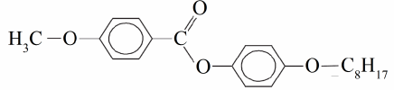
The compound selected for the studies, 4-n-octyloxyphenyl 4-n-methyloxybenzoate (1OO8), has nematic phase in the temperature range between 53 ∘C and 77 ∘C Salamon2013 . Its chemical structure is shown in Fig. 1. It has negative dielectric and positive conductivity anisotropies; hence standard EC develops at pure ac driving. At pure dc voltage, depending on the sample thickness and on the electrical conductivity, it exhibits either flexodomains Salamon2013 or standard EC.
The liquid crystal was filled into commercial cells ( m, WAT, Poland and m, EHC. Co, Japan); rubbed polyimide coatings on the transparent electrodes ensured a planar initial alignment of the nematic. The cell was placed into a temperature controlled compartment (a Linkam LTS350 hot-stage with a TMS 94 controller); experiments were performed at the temperature ∘C, i.e., well in the nematic phase range.
The voltage applied to the cell was provided by the function generator output of a TiePie Handyscope HS3 digital oscilloscope through a high voltage amplifier. It allowed to synthesize the driving voltage in the form of with arbitrary ratios. The two oscilloscope channels of the same device were used to record simultaneously the signals of the applied voltage and the current flowing through the cell, thus providing information on the sample impedance during pattern formation.
The voltage-induced patterns were observed by a polarizing microscope (Leica DM RXP) at white light illumination using a single polarizer (shadowgraph Rasenat1989 technique). An attached digital camera, Mikrotron EoSens MC1362, was used to record snapshot sequences for documentation and/or later digital processing. It was capable of high speed imaging at a variable (maximum 2000 frames/s) rate with a spatial resolution of 520*512 pixels at 256 grey levels. A specially designed trigger logic was applied to synchronize image recording of the high speed camera with the zero crossing of the ac component of the applied voltage. Thus the temporal behaviour could be monitored by taking 20–4000 snapshots (depending on ) within a driving period. Measurements were computer controlled using LabView.
Digital processing of the recorded images allowed determination of the wave vector of the pattern (using two-dimensional FFT) as well as of the pattern contrast which we defined as the mean square deviation of the intensity, (here is the intensity of a pixel, and denotes averaging over the whole image). This definition satisfactorily discriminates the initial (undistorted) and the patterned state, though it does not allow distinguishing between various pattern morphologies.
For the precise measurements of the sample impedance, a dielectric analyser (Novocontrol Alpha equipped with a ZG4 test interface) was also employed. In order to obtain the values of the anisotropy of the dielectric permittivity and the electrical conductivity, the thermostated sample (a commercial cell of m) was put into an electromagnet with the magnetic induction perpendicular to the confining electrodes, i.e., perpendicular to the initial planar director orientation . At , the components and (perpendicular to ) could be obtained. As the compound has a positive magnetic susceptibility anisotropy , increasing the magnetic field above a Freedericksz transition is induced resulting in a quasi-homeotropic state with the director orientation nearly parallel to the magnetic field at high , thus allowing to estimate the components and (parallel to ). Here is the vacuum permeability and is the splay elastic constant.
Unfortunately, due to , the dc bias voltage has a dielectric stabilizing effect acting against the magnetic field, hence increasing the magnetic Freedericksz threshold according to , where . In order to keep for large dc bias voltage, a cell with a thickness of mm was constructed. In this cell, the polyimide coating on the ITO electrodes was unrubbed, as at such a thickness the surface interactions cannot provide a uniform orientation in the bulk. Instead, during the impedance measurements the magnetic field was kept switched on continuously at and the cell was rotated alternately to the positions with parallel to the substrates ( and are measurable) and perpendicular to the substrates (yielding and ).
III Results
The planarly aligned 1OO8 exhibits flexodomains as a first instability at pure dc driving, while it shows EC patterns when driven with ac voltage Salamon2013 . In Section III.1 we explore how superposition of dc and ac voltages alters the pattern morphologies, the onset characteristics ( and ) and their frequency dependence, and up to what combination of the superposed voltages the uniform state can prevail. In Section III.2 our theoretical considerations are presented in comparison with the experimental findings. Finally we report in Section III.3 on the results of the conductivity measurements, that are essential for understanding the phenomena under scope.
III.1 Pattern morphologies and the stability limit curve
III.1.1 Superposition of ac and dc voltages
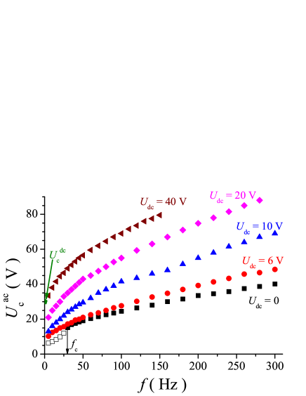
Figure 2 presents the frequency dependence of the ac threshold voltages of a m thick cell, for pure ac () as well as for different dc bias voltages up to V. For pure ac driving one sees the usual scenario of standard EC: conductive regime at low and dielectric regime above the crossover frequency Hz (see the vertical black arrow in Fig. 2).
Note that since 1OO8 exhibits flexodomains for pure dc voltage driving at V (green arrow in Fig. 2), there should exist a transition from the conductive EC roll pattern to FD as the ac frequency is reduced. This crossover occurs, however, at ultralow at a few mHz Salamon2013 , therefore it is not shown in Fig. 2.
Applying a small dc bias voltage, the crossover frequency is substantially reduced; for V only the dielectric regime becomes detectable for Hz. At a fixed frequency, the ac threshold voltage increases monotonically with the dc bias voltage.
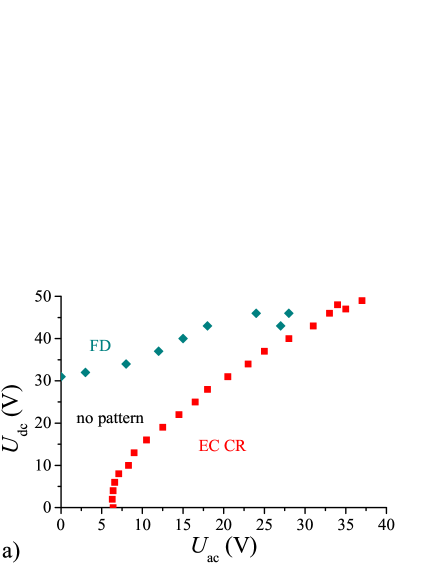
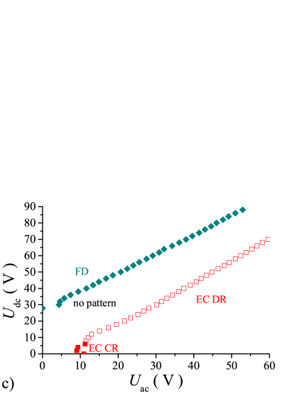
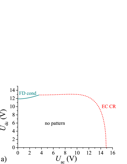
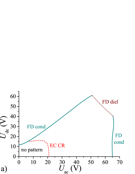
In Figs. 3(a)–3(c), we present the morphological phase diagrams (the SLC in the – plane) of the same cell for Hz, Hz and Hz, respectively. Though these figures resemble the ones obtained previously for Phase 5 (e.g. Figs. 1 and 2 of Salamon2014 ), we have to emphasize an important difference: the upper branch of the SLC here corresponds to the threshold of flexodomains (instead of the dc mode of EC).
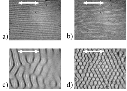
It can be seen that adding an ac voltage results in an increase of the dc FD threshold which becomes nearly linear for higher . This behaviour is in accordance with previous findings on FD in other nematics Marinov2006 ; Tadapatri2012 . Moving along this branch the type of the pattern (FD) remains unaltered [see Figs. 4(a) and 4(b)], only a decrease of the pattern wavelength can be observed. The lower branch of the SLC corresponds to conductive EC oblique rolls [see Figs. 4(c) and 4(d)]. It is seen that, in agreement with Fig. 2, increasing the dc bias voltage results in higher ac thresholds and also in some reduction of the pattern wavelength.
For low frequencies of the ac voltage component ( Hz, Fig. 3(a)), the two SLC branches join directly, representing a crossover from conductive EC to FD patterns at V and V.
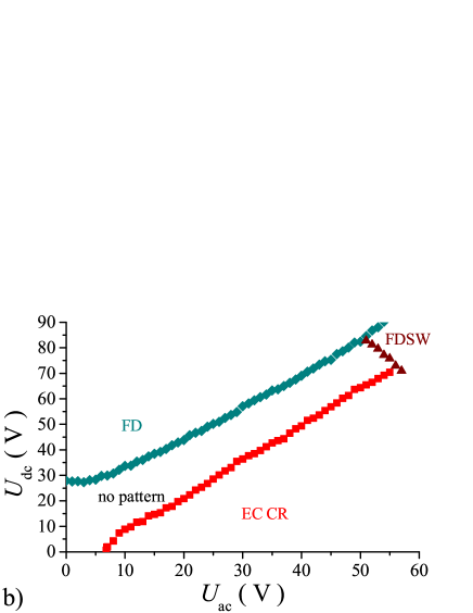
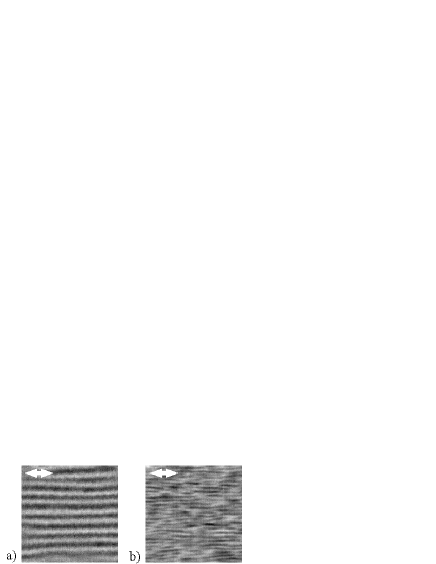
At Hz (Fig. 3(b)) the upper (FD) and lower (conductive EC) branches run almost parallel at higher voltages. In this case the SLC has a third, connecting branch which limits the pattern-free region. The pattern appearing here corresponds also to parallel stripes, but with a much lower contrast and much shorter wavelength than those of the FD along the upper branch; it is identified as another type of flexodomains (denoted as FDSW). As illustrations, Figs. 5(a) and 5(b) show snapshots of the FD and the FDSW patterns, respectively, at the same (higher) magnification after contrast enhancement. Outside the SLC, near to the crossing of the branches, there is a voltage range where FDSW may coexist with the usual FD. The two kinds of patterns occupy different locations; while FD is stationary, FDSW fluctuates with the driving voltage. Similarly, near the crossing of the EC and FDSW branches, FDSW may coexist with conductive EC rolls; in this case the patterns emerge at the same location, but in different time windows within the same driving period of the ac voltage (similarly to the ultralow behaviour of calamitic materials Salamon2013 ).
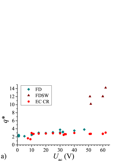
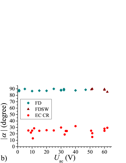
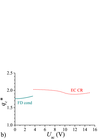
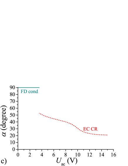
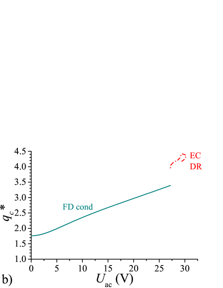
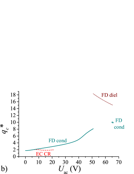
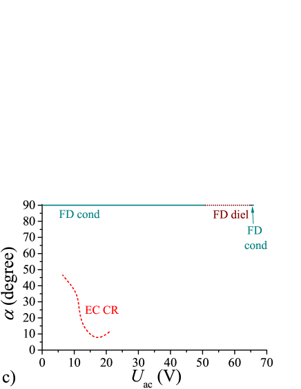
The change of the dimensionless wave number ( is the wavelength of the pattern) and the obliqueness angle at threshold (along the SLC) is depicted in Figs. 6(a) and 6(b), respectively. It can be seen that of FD and of the conductive regime of EC are very similar (–3.5) and depend only slightly on , while for FDSW one finds much larger values (–15) with a stronger dependence. In contrast to , the obliqueness angle is not affected by the FD–FDSW transition; both are parallel to . Note that for both kinds of flexodomains the apparent periodicity [the distance between subsequent dark stripes in Figs. 4(a)–(b) and 5(a)–(b)] corresponds to the half wavelength, while for EC in Figs. 4(c)–(d) black lines are repeated with the periodicity of the full wavelength.
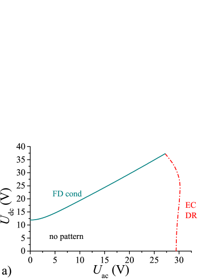
For a slightly higher frequency [ Hz, Fig. 3(c)], the morphological diagram is similar: the upper and lower branches of the SLC run nearly parallel. There is, however, a transition in the pattern type along the lower (EC) branch of the SLC. The conductive oblique rolls are seen only for V; for higher dc bias voltage the pattern switches to dielectric rolls yielding a jump in the wavelength of the pattern and also in the obliqueness (the dielectric rolls are normal to along the SLC). Another important difference is that at this , the two branches of the SLC are not connected within the experimentally accessible voltage range. The inhibition of pattern formation by superposing ac and dc voltages is so effective that no pattern appears at voltages exceeding several times the individual thresholds, e.g. at V combined with V.
For even higher frequencies the SLC looks similar to that in Fig. 3(c); except that the EC branch is shifted towards higher ac voltage and for Hz only dielectric rolls are observable.
III.1.2 Superposition of ac voltages of different frequencies
Besides exploring the behaviour at superposed ac and dc voltages, we have also tested what happens if two ac voltages ( and ) with substantially different frequencies (, respectively) are superposed. To have both frequencies in the conductive regime of EC, the crossover frequency had to be pushed above , which could be realized using thicker cells than in Section III.1.1.
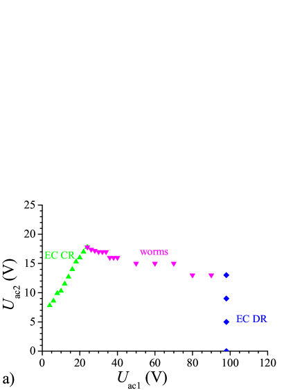
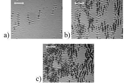
Figure 7(a) exhibits the morphological phase diagram of a m thick sample in the – plane for Hz and Hz. The SLC has three branches. Along the low frequency () branch, oblique rolls of conductive EC are seen and the threshold voltage is increasing upon superposing a voltage with high frequency. The high frequency () branch of the SLC is practically vertical; the threshold voltage of the dielectric EC occurring here is not altered by adding a lower frequency component. The pattern free region is closed by the third SLC branch running across the previous two ones, indicating sharp morphological transitions at the intersection points. Indeed, along this branch, the pattern is very different; instead of extended rolls, the pattern is rather localized to small regions in space, known as worms Dennin1996 ; Tu1997 ; Riecke1998 ; Bisang1999 . A sample snapshot is shown in Fig. 8(a). Increasing the low frequency voltage component while keeping constant, these worms serve as seeds for gradually extending the roll pattern to the full viewed area. This process is illustrated in Figs. 8(b) and 8(c). The slope of the threshold curve is slightly negative in this branch; adding a high voltage reduces the low threshold.
We note that a similar worm state has been reported in Pietschmann2010 , for the case when was chosen in the conductive regime and was above in the dielectric regime. This may imply that the condition is more important in inducing the worm scenario, than the actual value of the ratio.
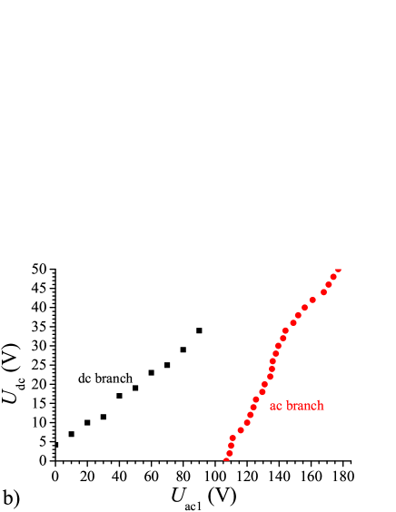
For comparison, the SLC for the superposition of ac and dc voltages is shown in Fig. 7(b). In this case, the two branches of the SLC let the pattern-free region extend to high , voltage combinations, similarly to the case shown in Fig. 3(c). These observations prove that the effective pattern inhibition is really a consequence of the applied dc voltage. Noticeably in Fig. 7(b), the ac branch (EC DR) of the SLC is shifted to much higher ac voltage compared to the cases in Fig. 3, due to the higher driving frequency, while the dc branch (EC CR) of the SLC appears at much lower dc voltage, as in this thicker sample EC occurs at dc driving instead of FD.
III.2 Theoretical considerations
As already mentioned in Section I, by now the theoretical description of electroconvection and of flexodomains (the extended SM) has been worked out for pure ac or dc drivings Krekhov2011 ; Krekhov2008 . Since the patterns emerge continuously from the initial state at onset (corresponding to a forward bifurcation), the onset characteristics ( and ) can be obtained from a linear stability analysis of the underlying nemato-hydrodynamic equations. The linearized equations and the details of the numerical procedure are presented in Krekhov2008 . In case of combined ac+dc driving the code used in Krekhov2008 has been modified by including the additional dc voltage (see Krekhov2014 for some examples of the onset calculations).
To compare the experimental results with the theoretical calculations, the following material parameter set of 1OO8 has been used; elastic constants: pN, pN, pN Salamon2013 ; viscosity coefficients (in lack of measurements MBBA values were taken): mPa s, mPa s, mPa s, mPa s, mPa s, mPa s; dielectric permittivities: , ; electrical conductivities: nS m-1, ; flexoelectric coefficients: pC m-1, pC m-1 and sample thickness: m.
The results of the calculations are shown in Figs. 9 and 10 for two scenarios; FD occur at dc driving, while at ac driving the EC regime is conductive (low ) or dielectric (high ), respectively. The main features of the SLC and the ac voltage dependence of the dimensionless critical wave number and the obliqueness angle strongly resemble those obtained for Phase 5 Krekhov2014 . Comparing the experimental curves in Figs. 3(a), 3(b) and 6 with the calculated ones in Figs. 9 and 10, we can see that the dc branch of the SLC follows the predictions: adding an ac component increases the dc threshold voltage as well as the critical wave number of FD. For the ac branch of the SLC, however, there is a mismatch between the theoretical predictions and the experimental findings. According to the calculations and also the qualitative analysis presented in Krekhov2014 , the dc voltage should reduce the ac threshold of EC in the conductive regime [see Fig. 9(a)], and in the dielectric regime the same reduction should occur after a minor initial increase [see Fig. 10(a)]. In contrast to that, in the experiments a substantial increase of the ac threshold upon dc bias was detected (for both conductive and dielectric EC), similarly to the recent findings on the nematic Phase 5 Salamon2014 .
The recent theoretical analysis of flexodomains Krekhov2011 has pointed out that in case of pure ac driving the equations have two solutions with different time symmetries: the conductive mode implies stationary modulation of the out-of-plane director component, while for the dielectric mode it oscillates with the ac frequency. The threshold voltages and critical wave numbers of the two solutions are different; which of them has a lower threshold depends on the flexoelectric coefficients, on the dielectric anisotropy, on the elastic constants and on the frequency of driving. For typical material parameter sets, conductive FD are expected for low , but dielectric ones for high . Nevertheless, the frequency induced transition from conductive FD to dielectric FD, theoretically predicted in Krekhov2011 , has not yet been reported, as FD are usually not observed at high due to their high threshold voltage, which is either unreachable experimentally or because EC sets in already at lower .
Adding a dc bias voltage breaks the time symmetry of the equations. However, the solution can be associated with one of the three (dc, conductive, or dielectric) modes according to the temporal dynamics of the out-of-plane director component in leading order.
In order to verify the possibility of the transition from conductive FD to dielectric FD under combined dc and ac driving, their stability diagram has been calculated for 1OO8 at an intermediate frequency Hz of the ac voltage component. The linear stability analysis of FD demonstrate that indeed, as can be seen in Fig. 11(a), the stability limiting curve has three branches: conductive FD (FDcond) starting from both the dc and the ac axes and a crossing branch of dielectric FD (FDdiel) at high dc and ac voltages. The wavenumber of FDcond increases with increasing [see Fig. 11(b)], but has a huge jump at the transition to FDdiel; in the FDdiel range one has a slope of opposite sign. For both kinds of flexodomains the stripes are parallel to [, see Fig. 11(c)], and the direction of does not alter with .
The material parameter studies show that the large elastic anisotropy of 1OO8, , is a prerequisite for the transition between two types of FD under combined dc and ac voltages. In fact, such transition has not been found in the calculations when using the material parameters of the nematic liquid crystal MBBA where . Note that considering in the calculations EC instability as well, the conductive EC threshold curve is located at much lower ac voltage than that for the flexodomains. The EC branch of the SLC in Fig. 11(a) as well as the behavior of the critical wave number and the obliqueness angle in Figs. 11(b)–(c) look very similar to that obtained at lower ac frequency (Fig. 9).
It is clearly seen that the voltage combinations belonging to the FDcond–FDdiel transitions are very high and are by far outside the SLC of EC; so normally it should not be observable. However, if EC is inhibited by some reason, the transition between the two types of FD may become accessible.
We think that actually this happened during the measurement presented in Fig. 3(b). Though the ac threshold of EC for 1OO8 at Hz is low at , applying a dc bias increases the ac threshold voltage enormously. The larger the dc bias voltage, the more the threshold increases. Finally, due to this effective inhibition of EC, the voltage range of the FDcond–FDdiel transition has been reached. We are convinced that the flexodomains marked FD in Fig. 3(b) correspond to the conductive type, while those marked with FDSW are a manifestation of flexodomains of the dielectric type. This statement is supported by the similarities of the theoretical and experimental SLCs as well as the qualitative (or even semiquantitative) agreement of the behaviour of the wave numbers at the FD–FDSW (i.e., at the FDcond–FDdiel) transition.
Summarizing, the outcome of the comparison of the experiments and the theory so far is that there is a good agreement along the whole SLC for low , as well as along the dc branch of the SLC at any . Nevertheless, a serious discrepancy is present for the ac branch of the SLC for high . In the following we attempt to tackle this problem.
III.3 Electrical conductivity measurements
The threshold voltages of the electric field induced patterns are governed by, besides the control parameters (the waveform, magnitude and frequency of the applied voltage) and the sample thickness, a set of temperature dependent material parameters, which include the dielectric permittivity, the electrical conductivity and their anisotropies, the elastic constants, the viscosities and the flexoelectric coefficients Kramer1996 ; Krekhov2008 . Most of these material parameters depend exclusively on the chemical structure of the compound and are expected to be identical for various samples kept under the same conditions. The electrical conductivity, however, originates in the ionic and electrolytic impurities. Therefore, the actual value of the conductivity and its anisotropy may vary from sample to sample depending on the concentration and type of charge carriers. In addition, the conductivity may change in time under applied voltage due to, e.g., reversible ionic adsorption at electrodes, irreversible ionic purification, charge injection Bazant2004 ; Gaspard1973 ; Murakami1997-1 ; Murakami1997-2 ; Huang2012 ; thus it may depend on the history of the sample. These conductivity variations may easily reach an order of magnitude. Therefore, it is important to obtain information on the conductivity at the time of pattern formation studies.
In order to conform to this requirement, the electric current flowing through the sample and the applied voltage signals were recorded simultaneously to image capturing. From the ac voltage and current components, the complex impedance of the cell (interpreted as a parallel RC circuit) was determined; it was phase sensitively decomposed into the parallel resistance and parallel capacitance of the cell. As planar samples were used, for voltages below the pattern onset, one finds and (here is the effective electrode area); that allows to determine the conductivity and dielectric permittivity . Above pattern onset, the resistance and the capacitance depend, in addition, on , on , on the director distortion and on the velocity field.
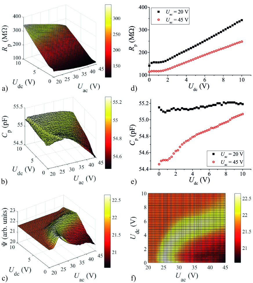
In Fig. 12, we present the results of the measurements on a m thick cell. Figures 12(a) and 12(b) depict the ac and dc voltage dependence of and , respectively, obtained during a voltage scan of a () area, which includes the ac branch of the SLC. Figures 12(d) and 12(e) show a cross-section at fixed . It can be seen that a dc bias voltage V causes a substantial, nearly linear increase of (a reduction of ), while increasing the ac voltage results in some decrease of [see also Fig. 12(d)]. On the contrary, remains nearly constant upon changing ; the maximal deviation (%) occurs in the range of small dc, but large ac voltages. This is, however, the range which is already much above the onset of EC (i.e., it is a turbulent state) and therefore director distortions are there non-negligible. This latter statement is supported by the morphological diagrams in Figs. 12(c) and 12(f), which depict the voltage dependence of the pattern contrast for the same voltage scan. Some decrease of the contrast at high ac and low dc voltages below the background of the undistorted state is expected to be due to turbulent light scattering.
As strong dependence of the conductivity on the dc bias voltage has been demonstrated in Figs. 12(a) and 12(d), further questions arise about the temporal dynamics of the conductivity change, and whether the anisotropy of the conductivity depends on the dc voltage too. To answer these questions, high precision impedance measurements were performed using a dedicated dielectric analyzer.
In a planar cell, and are the directly measurable quantities. In order to get information on the anisotropy, an additional magnetic field can be applied normal to the electrodes, in order to induce a splay Freedericksz transition into a quasi-homeotropic state. The threshold magnetic induction for the cells used in Sec. III.1.1 ( m) is T at ; thus the maximum applicable induction ( T) is too small for a reliable estimation of and . For the cell in Sec. III.1.2 ( m) one finds T at ; so the permittivity measured at the maximal is already much closer to , yielding . However, as the dc bias voltage has a dielectric stabilizing effect (), increases as the dc bias voltage is increased. Therefore, and similarly cease to be good approximations of and , respectively, for V.
In order to overcome this problem and allow studying the dc bias dependence of and in a wide voltage range ( V), a cell with mm was used. At such a thickness, without dc bias ; thus the magnetic field can provide a uniform bulk orientation . Therefore, rotating the cell in the high magnetic field alternately to the positions with parallel to and perpendicular to the substrates, , and , could be measured, respectively. The measurements were performed at kHz with a probing ac rms voltage of 0.2 V.
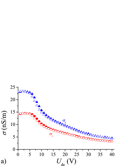
Figures 13(a)–(b) exhibit the dependence of and , and the relative conductivity anisotropy , respectively. The dc voltage was increased gradually in intervals of about 8 minutes; at each voltage the cell was repetitively rotated in the magnetic field of T in order to obtain the two components of the conductivity and permittivity. The solid and open symbols plotted at the same correspond to data measured at the beginning and at the end of these intervals, respectively.
It is clear from Fig. 13(a) that while the conductivity is unaffected by a small dc bias voltage ( V), it strongly reduces when increases. The same features could be seen before in Figs. 12(a) and 12(d), though there (in a thinner cell) the critical dc bias voltage, which induces conductivity variations was lower ( V). Meanwhile, both permittivity components remained unaffected by the dc voltage, indicating no dc bias induced change of the homogeneous planar or quasi-homeotropic director orientation. The relative conductivity anisotropy is presented in Fig. 13(b). It shows that not only the conductivity components, but too exhibit a monotonic decrease upon increasing : at V, is just half of its value at .
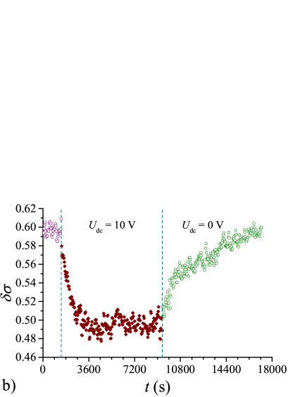
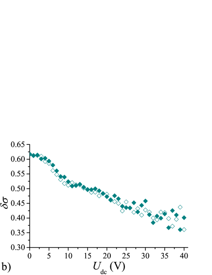
Dynamics of the dc voltage induced changes in the conductivity and in its anisotropy was also studied. Figures 14(a) and 14(b) exhibit the temporal evolution of the conductivities , , and the relative conductivity anisotropy , respectively, following a dc voltage jump from to V and vice versa, for the same mm thick sample. It is clearly seen that neither the change of the conductivity, nor of its anisotropy is instantaneous; instead, the dc voltage jump initiates a long lasting relaxation process, which is characterized by several time scales. The fastest one (not captured by the figures) is about seconds; the slower ones are from minutes to hours. For example, the curves in Fig. 14(a) could be well fitted (see the solid lines) by a superposition of two exponential decay curves:
| (1) |
where is the moment of the voltage jump. The time constants for the upward voltage jump were found as s, s, while for the downward voltage jump s, s. The curves clearly show that after two hours from the voltage jump the conductivity is still far from saturation and at longer time recordings additional, even longer time scales may become noticeable. These temporal changes one has to be aware of, even when the dc voltage dependence of the conductivity is measured by a voltage scan technique, as in Fig. 13.
We note that the temporal behavior of the conductivity in a thinner ( m thick) cell was very similar, except that the conductivity values were lower. Monitoring the conductivity variations there, following a dc voltage jump from to V and vice versa, s, and s were obtained and for the best fit a third, shorter time scale s was also necessary.
The relevant time scales for the reversible electrical response when a voltage is applied or removed are the relaxation time of the charge carriers , the transit (or migration) time and the diffusion time , where is the average mobility of the charge carriers, is the Boltzmann constant, and is the electronic charge Turnbull1973 ; Treiber1995 ; Bazant2004 . For a nematic layer of thickness m with the dielectric permittivity of , the conductivity of nS m-1 and typical values of the mobility m2 (V s)-1, one finds s, s, and s. The charge diffusion time characterizes the process of diffusion of slow charge carriers from the bulk into the depleted zones due to the electrical double layers formed at the electrodes at the time scale . The same time is typical for the equilibration of the charge distribution after the applied voltage is switched off. Clearly, is too small to be detectable with our experimental technique. The other two time scales, and , are however, in the order of the experimentally found characteristic times and .
Other processes, which are much longer in time, are the specific ionic adsorption and diffusion into the polyimide orienting layers covering the cell electrodes Huang2012 ; Murakami1997-1 ; Murakami1997-2 . Apart from the characteristic times of the reversible dynamics mentioned above, there are certainly some irreversible processes that can also be responsible for the long time conductivity variations shown in Fig. 14. These are ionic purification of the sample as well as possible decomposition of the nematic molecules and/or dissolution of impurity ions from the polyimide layers Gaspard1973 ; Murakami1997-2 .
The characteristic times given above are much longer than the typical acceptable waiting time between voltage steps in voltage scans. It means that scanning the – plane practically cannot occur under equivalent conditions for the conductivity, if dc voltage has ever been applied. As a consequence, measured at a particular (, ) combination may depend on the route of reaching that point as well as on the sample history (how large dc bias had been applied, when and for how long time). This means that exploring the – plane along horizontal lines (increasing at constant ) or along vertical lines (increasing at constant ) might not be equivalent.
IV Discussion
The increase of the ac thresholds of EC patterns upon applying dc bias voltage seen in Figs. 3 and 12(f) clearly does not match the theoretical predictions in Figs. 9(a), 10(a) and 11(a). The latter were calculated, however, in the framework of a model where and are independent of , while the experiments have proved that the conductivity and its anisotropy change substantially if a dc bias is applied.
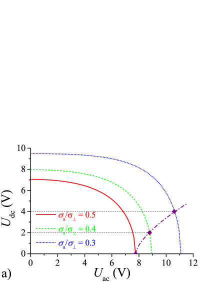
Although a dc-bias dependent conductivity is not captured by our extended SM model based on the Maxwell equations in the quasi-static approximation assuming ohmic conductivity of the nematic, one can verify the influence of various conductivity and/or conductivity anisotropy on the critical voltages of EC patterns. Note that the theoretical thresholds of flexodomains are independent of and , since for FD pattern one has resulting in .
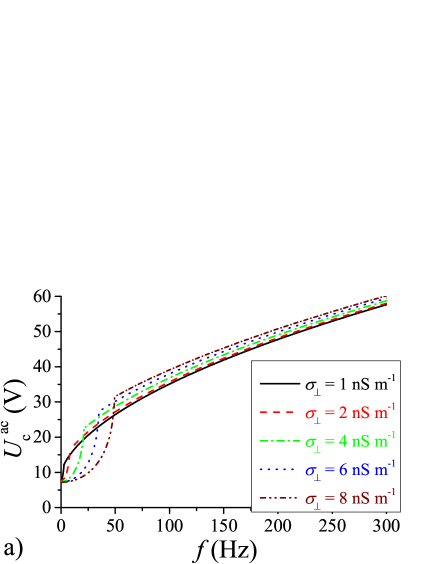
Figures 15(a)–15(c) show the frequency dependence of the threshold ac voltages , the dimensionless critical wave number and the obliqueness angle , respectively, for the conductive and dielectric regimes of EC at pure ac driving, calculated for the material parameter set of 1OO8 given in Section III.2, except and for different values taken from within the range found for thin samples. Similarly, Figs. 16(a)–16(c) show the frequency dependence of , and , respectively, however, for nS/m and various values.
First, in Figs. 15(a) and 16(a), one can notice that the crossover frequency of the transition from conductive EC to dielectric EC shifts toward lower either if or is diminished. This tendency may explain the experimentally found behaviour shown in Fig. 2: the dc bias yields the decrease of and finally the disappearance of the conductive regime via reducing the conductivity and/or its anisotropy. The dc-bias-induced conductive to dielectric transition observed at Hz [EC stability branch in Fig. 3(c)] is another manifestation of the same mechanism: the crossover frequency shifts from above to below the frequency of the ac voltage component due to the change in the conductivities.
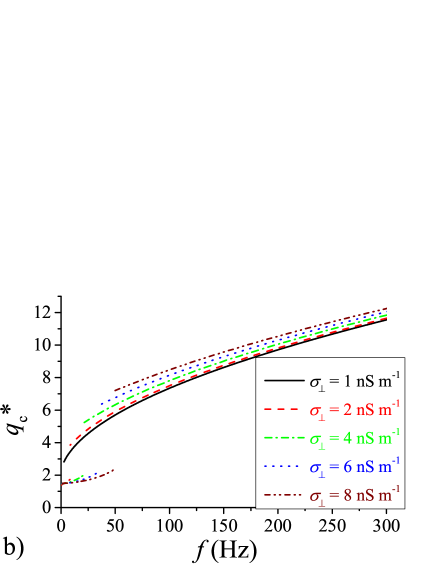
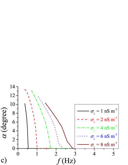
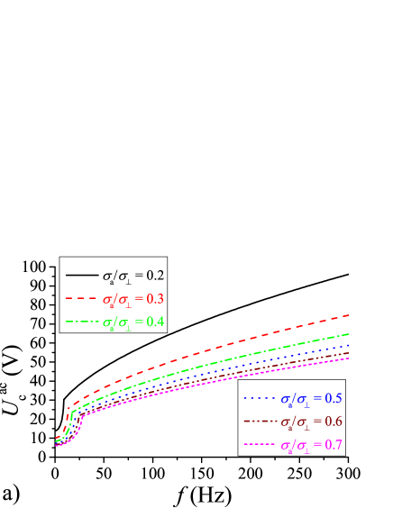
From Figs. 15(c) and 16(c), it follows that the Lifshitz–point (the frequency of the oblique-to-normal roll transition, where becomes 0) behaves in a similar way: shifts to lower values if either or diminishes.
Let us now focus on the threshold voltages and the wave numbers. It can immediately be perceived from Figs. 15(a) and 15(b) that the two EC regimes behave differently when changing . In the conductive regime, the reduction of leads to a substantial increase of , while in the dielectric one, it results in a minor reduction of the threshold. The critical wave number follows the same trend as the threshold: higher is accompanied by higher . In contrast to this, Fig. 16(a) shows that a reduction of yields an increase of both in the conductive and the dielectric EC regimes. According to Fig. 16(b), follows the trend of only in the conductive regime; in the dielectric one smaller results in smaller , in spite of the higher .
Knowing the behaviour without dc bias, one can also calculate the morphological phase diagram in the – plane for various and combinations. Figures 17(a) and 17(b) show, how the SLC is affected by , for low (conductive EC) and high (dielectric EC), respectively.
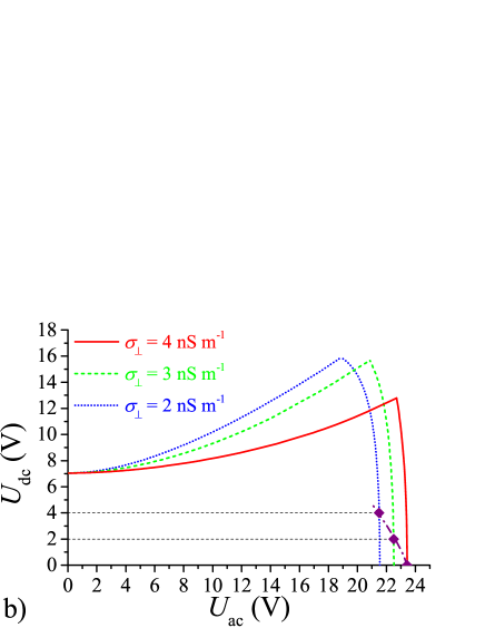
With Figs. 12(d) and 13(a) we have clearly proved that applying a dc bias voltage results in a reduction of . Therefore, if experimental data are going to be compared with the theoretical predictions, for each the theoretical , combinations should be taken from the corresponding (and thus different) stability limit curve, as shown by the diamond symbols in Fig. 17.
In the conductive regime, the SLC shifts to the right when becomes smaller. This results in an increase of the ac threshold voltage due to the dc-bias-induced conductivity reduction, which may overcome the small threshold decrease expected otherwise at fixed conductivity value [the dash-dotted line in Fig. 17(a) declines toward right]. This may qualitatively explain the experimentally found [see Fig. 3(a)] inhibition of the EC pattern formation upon applying dc bias voltage.
We note here that, as seen in Fig. 12(d), the dc-bias-induced conductivity reduction may be negligible for low dc bias voltage of –2 V. In such case the above mechanism does not play a role and so the threshold reduction predicted for constant should become effective. Indeed, it is seen in Fig. 12(f) that the EC branch of the SLC first declines toward left (smaller ) and turns back toward right (higher ) only for V.
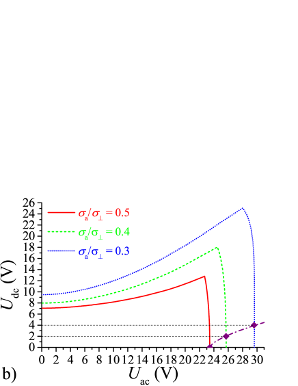
In contrast to the conductive one, in the dielectric regime the reduction of leads to the decrease of . Therefore the SLCs in Fig. 17(b) shift towards left upon decreasing . As a consequence, the procedure described above would reduce even more than expected for a constant [the dash-dotted line in Fig. 17(b) declines toward left].
A similar analyis can be done exploring the effect of the conductivity anisotropies. Figures 18(a) and 18(b) show, how the SLC is affected by , for low (conductive EC) and high (dielectric EC), respectively. It is seen that the trends are here similar both in the conductive and in the dielectric regimes: the SLC shifts upward and to the right upon the reduction of . This means that in the conductive regime the reduction of either or have similar consequences. In contrast, for the frequency of the ac voltage component in the dielectric regime, the SLC shifts to the left upon decreasing but to the right when reducing .
The impedance measurements have shown that, besides the conductivity value , the relative conductivity anisotropy is also affected by the dc bias; also reduces with increasing . It is seen in Figs. 18(a) and 18(b) that the diamonds corresponding to the thresholds taken from subsequent SLCs (corresponding to the diminishing relative conductivity anisotropy) indicate a net increase of upon increasing the dc bias voltage, for both the conductive and the dielectric regimes (the dash-dotted lines decline toward right for both cases), in agreement with the experimental curves in Fig. 3.
V Summary
In this paper we have reported about the effect of combined (ac+dc) driving on the electric field induced patterns in a nematic liquid crystal. We have found that the superposition of ac and dc voltages typically hinders the pattern forming mechanisms as it leads to an increase of the critical voltages. Consequently, the pattern-free region extends to voltages much above the pure ac or dc thresholds and closure of the stable region could only be observed at low frequencies. At high ac and dc voltages, a transition between two types of flexodomains could be observed, which is manifested in a sudden change in the wave number of the pattern. This transition could be identified as a crossover between flexoelectric domains of conductive and dielectric time symmetries.
We have found that under combined dc and ac driving, the increase of the critical dc voltage for flexodomains at increasing ac voltage component is well captured by the linear stability analysis of the extended standard model. In contrast, the increase of the ac threshold for EC patterns by a dc voltage bias is in contradiction with the theoretical predictions.
It is known from studies on isotropic weak electrolytes that application of a dc voltage may lead to charge depletion and to building up an electric double layer at the electrodes, which results in an inhomogeneous electric field with large gradients across the sample and a nonlinear current response Pikinbook ; Barbero2006 ; Derfel2009 . Nematics can also be regarded as (anisotropic) weak electrolytes, as their small electrical conductivity is originating from ionic contaminants. Thus the above effects may occur in nematics too. An experimental proof of their presence is the measured reduction of the sample’s conductivity upon application of dc bias voltage. The experiments proved that the relative anisotropy of the conductivity is also affected by the dc voltage.
In a lack of theoretical models for weak electrolytes capturing the reduction of the conductivity under application of dc bias voltage, we have analyzed the qualitative trends for the instability thresholds in the framework of the extended SM by varying the model parameters. For fixed values of the conductivity and the anisotropy of conductivity, the discrepancy between calculated EC instability curves and experiments is not surprising. We have shown, however, that when taking into account the experimentally found variations of the conductivity and its anisotropy due to the dc bias voltage, all peculiarities of the stability limiting curves for the EC instability can be qualitatively well reproduced.
ACKNOWLEDGEMENTS
Financial support by the Hungarian Scientific Research Fund (OTKA) grant No. NN110672 is gratefully acknowledged. We wish to thank M. Khazimullin for stimulating discussions and constructive comments on the manuscript, and V. Kenderesi for technical assistance in impedance measurements.
References
- (1) L. M. Blinov and V. G. Chigrinov, Electrooptic Effects in Liquid Crystal Materials (New York, Springer, 1996).
- (2) P. G. de Gennes and J. Prost, The Physics of Liquid Crystals (Oxford, Oxford Science Publications, 2001).
- (3) Flexoelectricity in Liquid Crystals. Theory, Experiments and Applications, edited by Á. Buka and N. Éber,(London, Imperial College Press, 2012).
- (4) L. K. Vistin’, Kristallografiya 15, 594 (1970) [Sov. Phys. Crystallogr. 15, 514 (1970)].
- (5) Yu. P. Bobylev and S. A. Pikin, Zh. Eksp. Teor. Fiz. 72, 369 (1977) [Sov. Phys. JETP 45, 195 (1977)].
- (6) A. Krekhov, W. Pesch, and Á. Buka, Phys. Rev. E 83, 051706 (2011).
- (7) L. Kramer and W. Pesch, in Pattern Formation in Liquid Crystals, edited by A. Buka and L. Kramer, (New York, Springer-Verlag, 1996) p. 221.
- (8) E. F. Carr, Mol. Cryst. Liq. Cryst. 7, 253 (1969).
- (9) W. Helfrich, J. Chem. Phys. 51, 4092 (1969).
- (10) A. Krekhov, W. Pesch, N. Éber, T. Tóth-Katona, and Á. Buka, Phys. Rev. E 77, 021705 (2008).
- (11) T. Tóth-Katona, N. Éber, Á. Buka, and A. Krekhov, Phys. Rev. E 78, 036306 (2008).
- (12) N. Éber, L. O. Palomares, P. Salamon, A. Krekhov, and Á. Buka, Phys. Rev. E 86, 021702 (2012).
- (13) T. John and R. Stannarius, Phys. Rev. E 70, 025202 (2004).
- (14) J. Heuer, R. Stannarius, and T. John, Mol. Cryst. Liq. Cryst. 449, 11 (2006).
- (15) D. Pietschmann, T. John, and R. Stannarius, Phys. Rev. E 82, 046215 (2010).
- (16) Y. Marinov, A. G. Petrov, and H. P. Hinov, Mol. Cryst. Liq. Cryst. 449, 33 (2006).
- (17) P. Tadapatri, K. S. Krishnamurthy, and W. Weissflog, Soft Matter 8, 1202 (2012).
- (18) P. Kumar, J. Heuer, T. Tóth-Katona, N. Éber, and Á. Buka, Phys. Rev. E 81, 020702(R) (2010).
- (19) L. E. Aguirre, E. Anoardo, N. Éber, and Á. Buka, Phys. Rev. E 85, 041703 (2012).
- (20) E. S. Batyrshin, A. P. Krekhov, O. A. Scaldin, and V. A. Delev, J. Exp. Theor. Phys. 114, 1052 (2012).
- (21) A. Krekhov, W. Decker, W. Pesch, N. Éber, P. Salamon, B. Fekete, and Á. Buka, Phys. Rev. E 89, 052507 (2014).
- (22) P. Salamon, N. Éber, B. Fekete, and Á. Buka, Phys. Rev. E 90, 022505 (2014).
- (23) P. Salamon, N. Éber, A. Krekhov, and Á. Buka, Phys. Rev. E 87, 032505 (2013).
- (24) S. Rasenat, G. Hartung, B. L. Winkler, and I. Rehberg, Exp. Fluids 7, 412 (1989).
- (25) M. Dennin, G. Ahlers, and D. S. Cannell, Phys. Rev. Lett. 77, 2475 (1996).
- (26) Y. Tu, Phys. Rev. E 56, R3765 (1997).
- (27) H. Riecke and G. D. Granzow, Phys. Rev. Lett. 81, 333 (1998).
- (28) U. Bisang and G. Ahlers, Phys. Rev. E 60, 3910 (1999).
- (29) M. Z. Bazant, K. Thornton, and A. Ajdari, Phys. Rev. E 70, 021506 (2004).
- (30) F. Gaspard, R. Herino, and F. Mondon, Mol. Cryst. Liq. Cryst. 24, 145 (1973).
- (31) S. Murakami and H. Naito, Jpn. J. Appl. Phys. Part 1 36, 773 (1997).
- (32) S. Murakami and H. Naito, Jpn. J. Appl. Phys. Part 1 36, 2222 (1997).
- (33) Y. Huang, A. Bhowmik, and P. J. Bos, J. Appl. Phys. 111, 024501 (2012).
- (34) R. J. Turnbull, J. Phys. D: Appl. Phys. 6, 1745 (1973).
- (35) M. Treiber and L. Kramer, Mol. Cryst. Liq. Cryst. 261, 311 (1995).
- (36) S. A. Pikin, Structural Transformations in Liquid Crystals (Gordon and Breach Science Publishers, 1991).
- (37) G. Barbero, G. Cipparrone, O. G. Martins, P. Pagliusi, and A. M. Figueiredo Neto, Appl. Phys. Lett. 89, 132901 (2006).
- (38) G. Derfel, J. Mol. Liq. 144, 59 (2009).