Tunneling Conductance in Normal-Insulator-Superconductor junctions of Silicene
Abstract
We theoretically investigate the transport properties of a normal-insulator-superconductor (NIS) junction of silicene in the thin barrier limit. Similar to graphene the tunneling conductance in such NIS structure exhibits an oscillatory behavior as a function of the strength of the barrier in the insulating region. However, unlike in graphene, the tunneling conductance in silicene can be controlled by an external electric field owing to its buckled structure. We also demonstrate the change in behavior of the tunneling conductance across the NIS junction as we change the chemical potential in the normal silicene region. In addition, at high doping levels in the normal region, the period of oscillation of the tunneling conductance as a function of the barrier strength changes from to with the variation of doping in the superconducting region of silicene.
pacs:
73.23.-b, 73.63.-b, 74.45.+c, 72.80.VpI Introduction
One of the most active research field in condensed matter physics since the last decade has been the study of Dirac fermions in graphene Geim and Novoselov (2007) and topological insulator Qi and Zhang (2011); Hasan and Kane (2010). The low energy spectrum of these materials satisfies massless Dirac equation. The relativistic band structure of the Dirac fermions has lead to tremendous interest in graphene in terms of possible application as well as from the point of view of fundamental physics.
Very recently, a silicon analogue of graphene, silicene has been attracting a lot of attention both theoretically and experimentally Ezawa (2015); Liu et al. (2011a); Lalmi et al. (2010); Padova et al (2010); Vogt et al. (2012), due to the possibility of new applications, given its compatibility with silicon based electronics. Unlike graphene, silicene does not have a planar structure; instead the buckled structure of silicene manifests itself as a spin-orbit coupling resulting in a band gap at the Dirac point Liu et al. (2011a). More interestingly, it has been reported earlier that such band gap is tunable by an external electric field applied perpendicular to the silicene sheet Drummond et al. (2012); Ezawa (2013a). This opens up the possibility of realizing silicene based electronics and very recently a silicene based transistor has been experimentally realized Tao et al. (2014).
In recent times, it has been realized that topologically non-trivial phases arise in silicene, tuned by the external electric field only Ezawa (2013a); Ezawa and Nagaosa (2013); Ezawa (2012). Graphene and silicene have similar band structures and the low energy spectrum of both are described by the relativistic Dirac equation i.e., both have the Dirac cone band structure around the two valleys represented by the momenta K and . However, the important difference between graphene and silicene is that the spin-orbit coupling (SOC) in silicene is much stronger than in graphene Liu et al. (2011a); Ezawa (2013a); Guzmán-Verri and Lew Yan Voon (2007) which causes the Dirac fermions in silicene to become massive. Furthermore, due to the buckled structure in silicene, the two sub-lattices respond differently to an externally applied electric field resulting in electrically tunable Dirac mass term Ezawa (2013a). Such tunability allows for the mass gap to be closed at some critical value of the electric field and then reopened. Hence, the phases on the two sides of the critical electric field where the gap is closed are different, with one of them being topologically trivial and the other being topologically non-trivial Ezawa (2013a); Ezawa and Nagaosa (2013); Ezawa (2012). As a result, silicene under the right circumstances can be a quantum spin hall insulator with topologically protected edge states Liu et al. (2011b); Ezawa and Nagaosa (2013); Ezawa (2013b).
The advent of superconductivity in graphene and certain topological insulators via the proximity effect has led to an upsurge of interest in this area Beenakker (2008); Qi and Zhang (2011). Very recently, superconducting proximity effect in silicene has been reported in Ref. Linder and Yokoyama, 2014 where the authors have investigated the behavior of Andreev reflection (AR) and crossed Andreev reflection (CAR) in a normal-superconductor (NS) and normal-superconductor-normal (NSN) junctions of silicene respectively.
In this article, we study the behavior of tunneling conductance (TC) in a normal-insulator-superconductor (NIS) junction of silicene where superconductivity in silicene is induced via the proximity effect. We model our NIS setup within the scattering matrix formalism Beenakker (2006); Blonder et al. (1982) and obtain the external electric field controllable TC for thin barrier limit. Similar set up in graphene have been studied earlier in Refs. Bhattacharjee and Sengupta, 2006; Bhattacharjee et al., 2007. However, TC based on silicene NIS structure has not yet been considered in the literature.
The remainder of this paper is organized as follows. In Sec. II, we present our model for the silicene NIS structure and describe the scattering matrix formalism to compute the tunneling conductance. In Sec. III, we present our results for the TC in the NIS set-up for the thin barrier case. Finally in Sec. IV, we summarize our results followed by the conclusions.
II Model and Method
In this section we will set up the equations to study the transport properties of an NIS junction in a silicene sheet placed along the -plane (see Fig. 1). The region is the normal region (N), the insulating region (I) has a width and occupies the region, while the superconducting region (S) occupies region. The insulating region has a gate tunable barrier potential of strength , while the superconductivity in region is assumed to have been induced via the proximity effect where the external superconductor is taken to be of the s-wave type.
The Silicene NIS junction is described by the Dirac Bogoliubov-de Gennes (DBdG) equation of the form
| (1) |
where is the excitation energy, is the proximity induced superconducting energy gap. The Hamiltonian describes the low energy physics near each of the K, Dirac points and has the form Linder and Yokoyama (2014),
| (2) |
where corresponds to K () valleys, is the fermi velocity (in the following we will set ), ( represents any of the N/I/S regions) is the chemical potential and is the spin orbit term. The Pauli matrices and act on the spin and sub-lattice space, respectively. The potential energy term owes its origin to the buckled structure of the Silicene wherein the and sites occupy slightly different planes (separated by a distance of length ) and therefore acquire a potential difference when an external electric field is applied perpendicular to the plane. It turns out that at the critical electric field each of the valleys become gapless with the gapless bands of one of the valley being up-spin polarized and the other down-spin polarisedEzawa (2013a); Ruchi Saxena and Rao (2015). Away from the critical field, the bands (corresponding to ) at each of the K and points are split into two conduction and two valence bands with the band gap being , where is a spin index.
Assuming translational invariance along the -direction we solve Eq. (1) to find the wave functions in all the three different regions. The wave functions for the electrons and holes moving along the direction in the N region are
| (3) |
where and is the energy of the particle wrt. to the Fermi level . We note that due to the spin being a good quantum number (and also because of time reversal symmetry) we can restrict our discussion by considering spin of only one type.
The conservation of momentum along the -direction, , leads to the angle of incidence and the Andreev reflection angle being related via, where
| (4) |
In the insulating region the wave functions are
where and
| (6) |
where and is the electrostatic potential that controls the barrier height.
Finally, in the superconducting region the wave functions of DBdG quasiparticles are given by,
| (7) |
where
| (8) |
As before, momentum conservation along the -direction relates the transmission angles for electron-like and hole-like quasi-particles via the following equation
| (9) |
for . The quasiparticle momentums are given by
| (10) |
where and is the gate potential applied in the superconducting region to tune the Fermi surface mismatch.
Let us consider an electron with energy incident on the interface of a conventional NIS junction of a silicene sheet. Part of the wave function gets transmitted and the rest undergoes both normal and Andreev reflection from the interface. Taking into consideration all these processes the wave functions in the different regions of junction can be written as Blonder et al. (1982):
| (11) |
where and are the amplitudes of normal reflection and Andreev reflection in the region, respectively. The transmission amplitudes and correspond to electron like and hole like quasiparticles in the region, respectively. From the continuity of the wave functions at the two interfaces we have
| (12) |
which yields a set of eight linearly independent equations. Solving them we obtain and , these amplitudes fully determine the tunnelling conductance of the NIS junction within the Blonder-Tinkham-Klapwijk formalism (BTK) Blonder et al. (1982)
where is the ballistic conductance of silicene.
III Thin barrier
In this section we will solve the scattering problem in the limiting case of thin barrier. We will consider the limit where the barrier height while the width such that the product is finite and non-zeroBhattacharjee and Sengupta (2006). We will consider only those scenarios wherein the mean-field criterion for superconductivity, i.e., , is satisfied. This can be achieved by controlling either the doping level or the gate voltage in the superconducting region. Solving the boundary condition (12) for and we obtain,
| (14) |
where
and
| (15) |
The remaining parameters are defined as follows,
| (16) |
where , and . Unless otherwise stated we consider a scenario wherein the product , and the upper conduction sub-band remains unfilled.
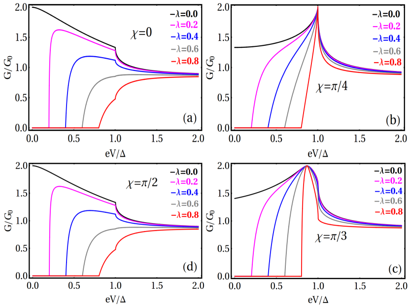
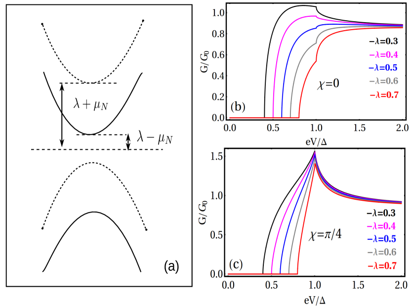
III.1 Undoped regime
In this subsection we focus on the undoped regime () in the normal side of the silicene sheet. The tunnel conductance value varies from to a peak value of with the Andreev reflection contributions being purely of the specular kind. The plot of as a function of for a fixed barrier strength and different ’s are shown in Fig. 2. For the transparent barrier regime (i.e., ) we obtain plots, Fig. 2a, identical to those in Ref. (Linder and Yokoyama, 2014). A common theme for vs for all the different barrier strengths [see plots Figs. 2(a)-(d)] is that the non-zero contribution to conductance arises when the incident electron has energy greater than the band gap.
Interestingly, this feature can be exploited by the electric field applied perpendicular to the plane which can then be used as a switch to turn on or off the conductance. Tuning the electric field so that brings the system to the Dirac limit and assures non-zero conductance at zero bias and for arbitrary strengths of the barrier. Another similarity between the different plots is the significant change in the slope at , this can be attributed to the sudden suppression of Andreev reflection for electron energies beyond the sub-gap regime.
We see from the plots Figs. 2(a)-(d) that the tunnelling conductance profile and the peak positions depend significantly on the barrier strength. Nevertheless, the profile remains unchanged for barrier strengths which differ by , i.e., for . This is understood by considering the simpler case of for which the reflection amplitude at an arbitrary incident angle has the expression
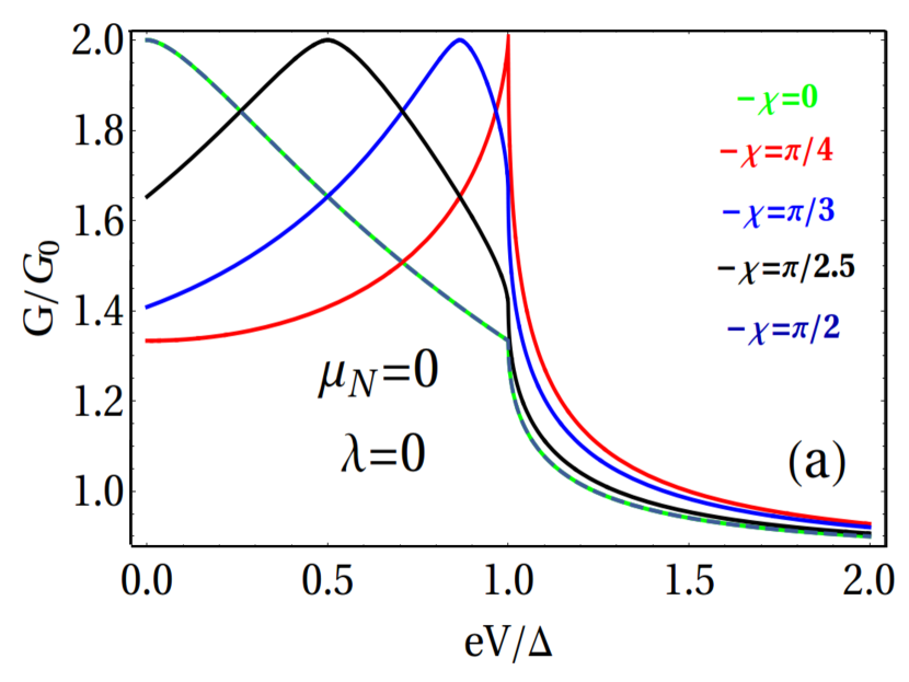
| (17) |
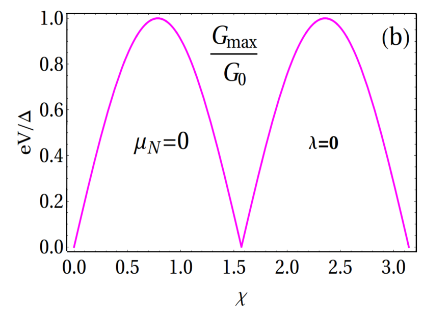
The above expression remains invariant for every that differs by integer multiple of . We also note that for the peak value of TC is [see Fig. 3(a)]which is achieved when the reflection coefficient vanishes, or in other words (follows from the unitarity criterion). This is realised for all incident angles when the transmission resonance criterion is satisfied, i.e., . In Fig. 3(b) we plot vs for which transmission resonance condition is satisfied.
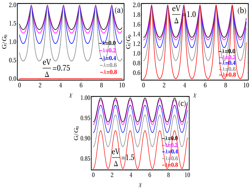
The oscillatory behavior of as a function of persists even for non-zero ’s. We plot this behavior in Figs. 4(a)-(c), where the plots are for a fixed and different ’s. As is expected, the peak value of is achieved for incoming electrons whose energy is below the sub-gap regime. However, the conductance can be made to switch off as illustrated in Fig. 4(a) with , by tuning the out of-plane electric field to . For absence of Andreev reflection implies the peak value (for ) to be at most [see Fig. 4(c)]. We note that the oscillatory dependence of on is in complete contradiction to the normal metal-insulator-superconductor junctions, where increasing the barrier strength always leads to the suppression of conductance Blonder et al. (1982).
For completeness we will consider a scenario wherein the chemical potential is non-zero, more specifically . Now, although electronic levels for exist, yet the conductance remains zero until the criterion is satisfied. This is due to the absence of Andreev reflection as there are no states available for hole reflection [see Fig. 5(a)]. We see this feature manifest itself in the vs plots in Figs. 5(b), (c). Note that unlike the case, now the transmission resonance criterion is not satisfied and the peak value of is smaller than .
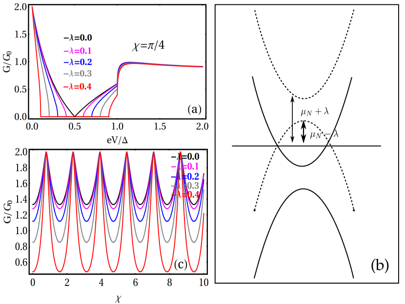
III.2 Moderately doped regime ()
Here we will focus on moderate doping levels which we define as and set . It turns out that the profile of vs plots as shown in Fig. 6(a) are markedly different from the earlier studied regimes. We find that the conductance at zero bias voltage starts out from a non-zero value and monotonically decreases to zero at . The conductance remains zero till , beyond which it increases monotonically till .
For bias voltages in the range , the Andreev scattering is accompanied by hole scattering of the usual retro type. On the other hand, when an electron with energy is incident on the interface of NS junction it gets completely reflected back due to the absence of hole states [Fig. 6(b)]. In a further twist, an incident electron with energy in the range is again Andreev scattered due to the availability of hole states. However, the holes now undergo specular reflection due to the change in sign of the curvature of hole spectrum.
The oscillatory feature in the vs plots are shown in Fig. 6(c). For the simple case of the expression for reduces to
| (18) |
At zero bias, , the condition for transmission resonance reduces to , so the first maxima is exhibited at .
III.3 Highly doped regime
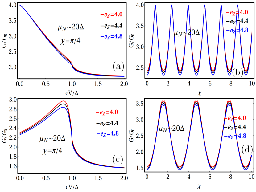
In this subsection we present our tunneling conductance (TC) results for the highly doped regime i.e., . The mean field criterion, , is now automatically satisfied irrespective of the value of . We will consider two scenarios, and , and plot vs and vs in the two regimes. Since , both the bands in normal region are occupied and will contribute to the conductance.
Due to the large value of the chemical potential the TC is nearly insensitive to the variation in and thus on the electric field applied perpendicular to the surface . However, the TC shows interesting behaviour in the two extreme regimes for . For large the TC exhibits, as before, a change in the slope of vs curve at for all barrier strengths [Fig. 7(a)]. Also, the periodicity in the dependence of the TC on the barrier strength persists [Fig. 7(b)]. For small a similar change in slope at is present in vs plots, however, the TC now exhibits periodicity as a function of [see Figs. 7(c)-(d)].
When is large (), there is a large Fermi wave-length mismatch between the normal and the superconducting side. In this scenario, we obtain the periodicity in the dependence of the TC on the barrier strength . On the other hand, for small (), Fermi wave-length mismatch turns out to be negligible between the two sides. This gives rise to the periodicity Bhattacharjee and Sengupta (2006) in the behavior of TC with respect to .
IV Summary and conclusions
To summarize, in this article, we have presented a theory of tunneling conductance of a Normal-Insulator-Superconductor (NIS) junction of silicene in the thin barrier limit. We have demonstrated that in this limit the tunneling conductance shows novel periodic behavior as a function of barrier strength. In particular, we note that the period of oscillation changes from () to () with the variation of doping in the superconducting side of silicene. Moreover, for the undoped regime (), the external electric field can be used as a switch to tune the conductance from on to off condition. The latter is a unique feature of silicene.
As far as experimental realization of our silicene NIS set-up is concerned, it can be possible to realize a proximity induced superconducting gap in silicene by using -wave superconductor like Heersche et al. (2007). Typical spin-orbit energy in silicene is while the buckling parameter Liu et al. (2011a); Ezawa (2013a). Considering Ref. Heersche et al., 2007, typical induced superconducting gap in silicene would be . For such induced gap, the change of periodicity of TC from to may be possible to observe by changing the doping concentration from to for a barrier of thickness and height which can be considered as thin barrier. Also the typical range of the external electric field can be within to use our set-up as a switch.
We expect our results to be qualitatively similar to the recently discovered two-dimensional materials like germenene, stanene Ezawa (2015); Dávila et al. (2014); Zhu et al. (2015). Although the strength of Rashba spin-orbit coupling in these materials can be stronger than silicene Liu et al. (2011a); Ezawa (2013a).
References
- Geim and Novoselov (2007) A. K. Geim and K. S. Novoselov, Nat. Materials 6, 183 (2007).
- Qi and Zhang (2011) X. L. Qi and S. C. Zhang, Rev. Mod. Phys. 83, 1057 (2011).
- Hasan and Kane (2010) M. Z. Hasan and C. L. Kane, Rev. Mod. Phys. 82, 3045 (2010).
- Ezawa (2015) M. Ezawa, J. Phys. Soc. Jpn. 84, 121003 (2015).
- Liu et al. (2011a) C. C. Liu, H. Jiang, and Y. Yao, Phys. Rev. B. 84, 195430 (2011a).
- Lalmi et al. (2010) B. Lalmi, H. Oughaddou, H. Enriquez, A. Kara, S. Vizzini, B. Ealet, and B. Aufray, Appl. Phys. Lett. 97, 223109 (2010).
- Padova et al (2010) P. D. Padova et al, Appl. Phys. Lett. 96, 261905 (2010).
- Vogt et al. (2012) P. Vogt, P. D. Padova, C. Quaresima, J. Avila, E. Frantzeskakis, M. C. Asensio, A. Resta, B. Ealet, and G. L. Lay, Phys. Rev. Lett. 108, 155501 (2012).
- Drummond et al. (2012) N. D. Drummond, V. Zólyomi, and V. I. Falko, Phys. Rev. B. 85, 075423 (2012).
- Ezawa (2013a) M. Ezawa, New J. Phys. 14, 033003 (2013a).
- Tao et al. (2014) L. Tao, E. Cinquanta, D. Chiappe, C. Grazianetti, M. Fanciulli, M. Dubey, A. Molle, and D. Akinwande, Nat. Nanotech. 10, 227 (2014).
- Ezawa and Nagaosa (2013) M. Ezawa and N. Nagaosa, Phys. Rev. B. 88, 121401(R) (2013).
- Ezawa (2012) M. Ezawa, Eur. Phys. J. B 85, 363 (2012).
- Guzmán-Verri and Lew Yan Voon (2007) G. G. Guzmán-Verri and L. C. Lew Yan Voon, Phys. Rev. B. 76, 075131 (2007).
- Liu et al. (2011b) C. C. Liu, W. Feng, and Y. Yao, Phys. Rev. Lett. 107, 076802 (2011b).
- Ezawa (2013b) M. Ezawa, Phys. Rev. B. 87, 155415 (2013b).
- Beenakker (2008) C. W. J. Beenakker, Rev. Mod. Phys. 80, 1337 (2008).
- Linder and Yokoyama (2014) J. Linder and T. Yokoyama, Phys. Rev. B. 89, 020504(R) (2014).
- Beenakker (2006) C. W. J. Beenakker, Phys. Rev. Lett. 97, 067007 (2006).
- Blonder et al. (1982) G. Blonder, M. Tinkham, and T. M. Klapwijk, Phy. Rev. B 25, 4515 (1982).
- Bhattacharjee and Sengupta (2006) S. Bhattacharjee and K. Sengupta, Phys. Rev. Lett. 97, 217001 (2006).
- Bhattacharjee et al. (2007) S. Bhattacharjee, M. Maiti, and K. Sengupta, Phys. Rev. B 76, 184514 (2007).
- Ruchi Saxena and Rao (2015) A. S. Ruchi Saxena and S. Rao, Phy. Rev. B 92, 245412 (2015).
- Heersche et al. (2007) H. B. Heersche, P. Jarillo-Herrero, J. B. Oostinga, L. M. K. Vandersypen, and A. F. Morpurgo, Nature 446, 56 (2007).
- Dávila et al. (2014) M. Dávila, L. Xian, S. Cahangirov, A. Rubio, and G. Le Lay, New J. Phys. 16, 095002 (2014).
- Zhu et al. (2015) F.-f. Zhu, W.-j. Chen, Y. Xu, C.-l. Gao, D.-d. Guan, C.-h. Liu, D. Qian, S.-C. Zhang, and J.-f. Jia, Nat. Mat. 14, 1020 (2015).