Ferroelectricity-induced asymmetrical two-dimensional electron gas in superlattices consisteing of insulating GdTiO3 and ferroelectric BaTiO3
Abstract
Two-dimensional electron gas due to semiconductor interfaces can have high mobility and exhibits superconductivity, magnetism, and other exotic properties that are unexpected in constituent bulk materials. We study crystal structures, electronic states, and magnetism of short-period (BTO)m/(GTO)2 (=2 and 4) superlattices consisting of ferroelectric BaTiO3 (BTO) and ferrimagnetic insulating polar GdTiO3 (GTO) by first principles calculations. Our investigation shows that the middle Ti-O monolayer in the GTO layer becomes metallic because the ferroelectricity in the insulating BTO layer induces an inhomogeneous electric field against the polarity-produced electric field in the GTO layer and thus differentially changes the d energy levels of the three Ti-O monolayers related with the GTO layer. Through avoiding electron reconstruction, the ferroelectric polarization also makes the electronic states and magnetism of two interfacial Ti-O monolayers become substantially different from those in the GTO/SrTiO3 superlattices without ferroelectricity. Such superlattices are interesting for potential spintronics applications because of their unique asymmetrical two-dimensional electron-gas properties and possible useful spin-orbit effects.
pacs:
75.70.-i, 75.75.-c, 73.20.-r, 68.65.-kI Introduction
Perovskite heterostructures often exhibit unusual physical properties that are absent in the constituent bulk materials a1 ; a2 . It is well known that two-dimensional electron gases (2DEG) can be formed at LaAlO3/SrTiO3 interfaces and such 2DEG can have high mobility and exhibit superconductivity, magnetism, and other exotic properties that are unexpected in the corresponding bulk materials a3 ; a4 ; a5 . 2DEG at interfaces between Mott insulators and band insulators have attracted significant attention. Stoichiometric GdTiO3 (GTO) is a Mott-Hubbard insulator that has a gap of 1.8 eV in terms of photoluminescence measurements.1 In bulk GTO, the ferromagnetic (FM) Ti array is antiparallel to the FM Gd array, resulting in a net ferrimagnetism with Curie temperature TC of 32 K.2 ; 3 ; 4 Compressive strain can make the ferromagnetic ordering of the Ti atoms change into a G-type antiferromagnetic (AFM) ordering on the LaAlO3 substrate and A-type AFM ordering on the YAlO3 substrate.5 The transport measurements of the 2DEGs at SrTiO3(STO)/LaTiO3(LTO) and STO/GTO interfaces exhibit an interfacial density values with the order of cm-2, approximately 1/2 electron per surface unit cell, which are essentially those predicted by electronic reconstruction.8 ; 9 ; 10 ; 11 This electronic reconstruction implies that when a LTO (or GTO) is combined with STO, the Ti cation in the TiO2 atomic layers between LaO (or GdO) and SrO monolayers actually has an averaged valence of 3d0.5.12 ; 13 ; 14 A charge modulation of over cm-2 electrons in 2DEGs formed in STO/GTO heterostructure field-effect transistors has been reported.15 ; 16 Recently, it has been shown, through combining experiment and theory, that in short-period STO/GTO superlattices, the GTO layer is insulating and non-polar, and conduction electrons are located in the STO layer, at neither of the two interfacial Ti-O monolayers.11
In order to achieve better 2DEG, however, we use ferroelectric BaTiO3 (BTO)6 ; 7 instead of STO to construct our (BTO)m/(GTO)2 superlattices, and then study the crystal structures and electronic properties of the superlattices with = 2 and 4 because the BTO ferroelectricity can survive in high-quality ultra-thin BTO layers30a . Our calculation and analysis show that both the ferroelectricity in the BTO layer and the polarity in the GTO layer survive through helping each other. The interfacial properties are substantially influenced by the ferroelectricity, charge polarity, and electronic correlations. We found that charge carriers are located not in the ferroelectric BTO layer, but in the two Ti-O monolayers related with the polar GTO layer. In the absence of electron reconstruction, the two interfacial Ti-O monolayers have very different magnetic moments and conductive properties. These imply that the 2DEG can be manipulated through controlling the direction of the ferroelectric polarization. Therefore, such superlattices are very interesting for designing switchable functional devices. More detailed results will be presented in the following.
II Computational details
Our first-principles calculations are performed using the projector-augmented wave method within the density-functional theorydft1 ; dft2 , as implemented in the Vienna Ab-initio Simulation Package (VASP).17 ; 18 The plane wave energy cutoff is set to 600 eV. For the exchange-correlation potential, we use the generalized gradient approximation (GGA) by Perdew, Burke, and Ernzerhof.19 The rotationally invariant GGA+U method is employed with and eV for Ti 3d and and eV for Gd 4f electrons.20 ; 21 The cell volume is relaxed and the ionic positions are optimized using a -centered k-grid. The electronic structure calculations were performed by using a -centered k-grid. Our convergence standard requires that the Hellmann-Feynmann force on each atom is less than 0.01 eV/Å. The convergence standard for the total energy is chosen to be eV.
III Results and discussion
III.1 Optimized structures
Band insulator BTO exhibits room-temperature ferroelectric phase with a semiconductor gap of 3.27 eV. 6 ; 7 In the GTO (001) direction, Gd3+O2- and Ti3+O monolayers appear alternately, carrying formal +1 and -1 charges, respectively, but in the non-polar BTO (001) direction both Ba2+O2- and Ti4+O monolayers are charge neutral. Moreover, both GTO and BTO share a common constituent, the TiO2 atomic layer (Ti-O monolayer). The paraelectric cubic BTO has space group Pm3m with experimental lattice constant of 4.00 Å and the BTO (001) layer has periodicity with experimental lattice constant of 5.65 Å.22 Bulk GTO has an orthorhombic Pbnm structure with experimental lattice constants of Å, Å, and Å, and the GTO (001) layer has periodicity.23 Thus, the mismatch amounts to 4.71% and 0.71% for the and axes. The optimized lattice constants are Å, with of 5.74 Å, for BTO, and Å, Å, and Å for GTO, consistent with previous calculation values.1
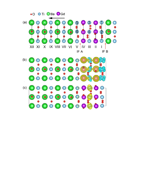
The optimized structure of (BTO)4/(GTO)2 is shown in Fig. 1(a). The optimized lattice constants are Å and Å for (BTO)4/(GTO)2, meaning a compressive strain of 1.23% in the axis for the BTO layer and a tensile strain of 3.77% for the GTO layer. There is a zero strain in the axis for the BTO layer and a tensile strain of 0.87% for the GTO layer. The calculated band gap of bulk GTO is 2.27 eV, consistent with previous calculation values1 and slightly greater than that of 2.02 eV calculated by a hybrid functional.24 The optimized result for the (BTO)2/(GTO)2 superlattice turns out to be very similar to that of the (BTO)4/(GTO)2 superlattice and hence we shall not present its detail. The magnetic moment value of each atom in the (BTO)4/(GTO)2 is visualized in Fig. 1(b). It can be seen that each Gd atom has the large positive magnetic moment value of 7.03 , but the magnetic moments of Ti atoms at sites 3 and 4 in the III monolayer are close to zero because of the mutual cancellation of contributions from different occupied states. We show in Fig. 1(c) the charge density distribution from the energy window between -0.5 and 0 eV. It is clear that the major part comes from the Ti-O monolayer labelled with ’III’ in the GTO layer.
| layer | monolayer | ||||
|---|---|---|---|---|---|
| GTO | I | -0.12 | -0.14 | ||
| II | -0.14 | -0.17 | |||
| III | -0.07 | -0.09 | |||
| IV | -0.07 | -0.08 | |||
| BTO | V | -0.11, 0.40 | -0.12, 0.38 | ||
| VI | 0.18 | 0.16 | |||
| VII | 0.05, 0.18 | 0.06, 0.13 | |||
| VIII | 0.10 | 0.10 | |||
| IX | 0.09, 0.11 | - | |||
| X | 0.09 | - | |||
| XI | 0.06, 0.14 | - | |||
| XII | 0.07 | - |
Table I gives the Ba-O and Ti-O polar displacements along the axis. The black arrow in Fig. 1 indicates that the net polarization of the BTO layer points leftward. The largest polar displacement per monolayer, (-0.11 and 0.40 Å), occurs at the interfacial Ti-O monolayer labelled with ’V’ in Fig. 1, the next largest one (0.18 Å) at the adjacent Ba-O layer labelled with ’VI’, and the polar displacements of other Ti-O and Ba-O monolayers are near 0.10 Å, which can weaken the polar discontinuity at the interfaces (IFA and IFB). Besides, we also found the polar displacement along the axis of Ti, Gd, and O in the GTO layer. In each monolayer, the Ti and Gd ions move rightward with respect to the neighboring O ions, which can reduce the diverging electrostatic potential in the GTO layer. The averaged displacements in each monolayer of the GTO layer are given in Table I. Because the ferroelectricity in BTO is originated from ionic displacements, these polar displacements, with the latest experimental results in high-quality ultra-thin BTO layers30a , make us believe that the ferroelectricity truly exists in the BTO layer, and coexists with the conducting layers in these BTO/GTO superlattices. The ferroelectric polarization in the BTO layer can produce an electric field in the GTO layer, hindering the electronic reconstruction like that in LTO/STO and STO/GTO. Therefore, in the (BTO)4/(GTO)2 superlattice, there is only small amount of electrons per Ti atom in the interfacial Ti-O monolayer labelled with ’V’ (including the Ti atoms labelled with ’5’ and ’6’) in Fig. 1(c), and these electrons populate the majority-spin dxy states, resulting in the dxy states splitting off the dzx and dyz states, as shown in Fig. 2, and a small magnetic moments of per Ti atom in this monolayer.
III.2 Monolayer-resolved electronic structures
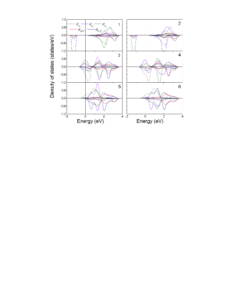
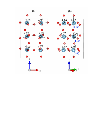
In Fig. 2 we also present the orbital-resolved density of states (DOS) of Ti atoms in the Ti-O monolayers labelled with ’I’ and ’III’ in (BTO)4/(GTO)2 superlattice. It is clear that in the two monolayers, the dyz and dzx orbitals appear alternately at every second Ti atom in each of the Ti-O monolayers. This type of orbital ordering was observed experimentally in the ferromagnetic YTiO3 through NMR 25 ; 26 , polarized neutron diffraction27 , and resonant x-ray scattering28 . In Fig. 3, we present the O-O distances over the bridging Ti atom for the three Ti-O monolayers. The O-O distance of 3.95 Å (near the Ti atom labelled with ’5’) along the axis, shorter than those of 4.09 and 4.07 Å along the and axes, causes the dxy orbital to have the lowest energy level for these two Ti atoms. The TiO6 octahedron in the GTO layer is elongated along the direction at sites 1 and 3, while they are elongated along the direction at sites 2 and 4, which can be seen by comparing Fig. 3(a) and 3(b). At sites 1 and 2, the occupied minority-spin states are mainly dyz or dxz orbital because the much longer O-O distances of 4.26 and 4.32 Å along the (or ) and direction than the O-O distance of 4.01 Å along the (or ) reduces the repulsive potential from the surrounding O ions in these two directions. These two Ti atoms contribute -0.88 and -0.89 to the magnetic moment, respectively, and there is an energy gap of 2.0 eV across the Fermi level. These magnetic moment values are consistent with the bulk value of -0.89 . The occupation of the majority-spin dxz, dxy, and dyz and the minority-spin dxy and d result in the net magnetic moments of 0.01 and -0.03 for the Ti atoms at sites 3 and 4, respectively. From Fig. 3(b), it can be seen that the O-O distances in the (or ) and (or ) directions are 4.27 and 4.22 Å, respectively, and the distance difference between the two directions is 0.05 Å. It should be pointed out that in this Ti centered octahedron, the O-O distance in the direction is shortened by 0.25 and 0.20 Å compared to those in the (or ) and (or ) directions. As a result, there are no occupied d states for these two Ti atoms because of their high energy levels.
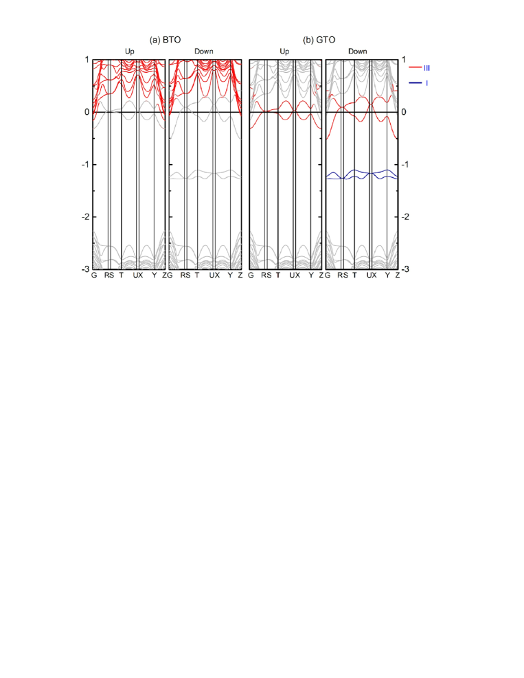
Fig. 4 displays the spin-resolved band structure of the (BTO)4/(GTO)2 superlattice. It can be seen that the system shows metallic property. The filled parts of the red bands in Fig. 4(a) are mainly originated from the Ti atoms in the V monolayer (near one interface), and the red and royal bands in Fig. 4(b) mainly from the Ti atoms of the III monolayer and the I monolayer (near the other interface). It is clear that the bands at the Fermi level are mainly from the Ti atoms at sites 3 and 4 in the III Ti-O monolayer, and a little part of the bands from the Ti atoms in the V monolayer. Therefore, the metallic feature of this system is mainly from the conductive Ti-O monolayer within the GTO layer, plus a little from one of the interfacial Ti-O monolayers, which is visually shown in Fig. 1(c). This phenomenon is interesting for spintronics applications because of the special 2DEG in the GTO layer. Our calculated results show that these 2DEG systems are almost the same for = 4 and 2. It can be reasonably believed that the main 2DEG feature should remain the same when the parameter becomes larger than 4.
III.3 Further insight
In bulk GTO, the FM Ti array is antiparallel to the FM Gd array and the AFM Gd-Ti interactions were reported to be weaker than the FM Ti-Ti interactions.3 ; 4 The spin-exchange along the axis in the perovskite Ti oxide TiO3 (where represents the trivalent rare-earth ions) changes from AFM to FM with increasing GdFeO3-type distortion, with the transition occurring at GTO.29 For sites 1 and 2 in the ’I’ monolayer, the orbitals of neighboring Ti atoms in the -plane are approximately orthogonal to each other. Hence, the FM spin configuration is favored through the Hund’s-rule coupling. The various GdFeO3-type distortions for Ti centered octahedral leads to the FM or AFM spin arrangement along the axis for Ti atoms. In Table II, we present the Ti-O bond lengthes and Ti-O-Ti bond angles in the I, III, and V monolayers. For the I monolayer, the Ti-O bond lengthes are so anisotropic that the oxygen octahedron is substantially distorted, causing the dxz or dyz split from the other d orbitals. For the III and V monolayers, the distorted oxygen octahedra are also consistent with the electronic structure feature. The Ti-O-Ti bond angle of 144.1∘, across the I, II, and III monolayers, is larger than that of bulk value of 139.5∘. This means the magnitude of the GdFeO3-type distortion of the GTO layer is weaker than that in bulk GTO due to the tensile strain of 3.77% in the axis for the GTO layer and the rearrangement of ionic positions, resulting in spin exchange along the axis being AFM. For Ti atoms in the Ti-O monolayer labelled with ’III’ in the GTO layer, the coordination number of Ti with d1 reduces by half, but that of Gd in the adjacent Gd-O monolayers is not changed. Therefore, for these Ti atoms, the co-existing antiparallel Gd-Ti and Ti-Ti couplings lead to the occupation of different orbitals in different spin channels in the same energy range near the fermi level.
| GTO bulk | superlattice | |||
| - | I | III | V | |
| 2.14, 2.06 | 2.09, 2.18 | 2.13, 2.14 | 2.03, 2.06 | |
| 1.96, 2.06 | 2.11, 2.12 | 1.92, 2.18 | ||
| 2.08 | 2.22 | 1.98 | 2.02 | |
| 2.13 | 2.05 | 1.96 | ||
| 143.3 | 151.5, 155.4 | 143.0, 143.1 | 162.2, 158.1 | |
| 139.5 | 172.9, 144.1 | 144.1, 147.1 | 147.1, 171.5 |
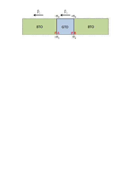
It can be seen from the band structure and the density of states that the two interfacial Ti-O monolayers are very different from each other. The I monolayer has one d electron per Ti atom and thus its Ti atom assumes +4 valence, but The Ti atom in the V monolayer approximately has +3 valence. This implies that there is no electron reconstruction between the interfaces in this case. It is in contrast to the STO/LTO and STO/GTO interfaces where an electron reconstruction happens, meaning that 1/2 electron per Ti atom is transferred from one interfacial Ti-O monolayer to the other.8 ; 9 ; 10 ; 11 ; 12 ; 13 ; 14 Without electron reconstruction, the LTO and GTO layers are polar in the z axis, and after the electron reconstruction, they become non-polar in the z axis. In our case, the GTO layer remains polar because there is no electron reconstruction! This result can be explained in terms of our calculated results by using Fig. 5. The polar GTO layer has a polarization vector and it induces virtual interfacial charges at the two interfaces (IFA and IFB). The ferroelectric BTO layer has a polarization vector which is parallel to . induces the two interfacial charges, and , at the two interfaces, but and are opposite to the interfacial charges from . Therefore, the interfacial charges and the intrinsic electric field in the GTO layer are substantially weakened due to the ferroelectric polarization, which avoids electron reconstruction between the two interfacial Ti-O monolayers and thus makes the asymmetrical 2DEG and should achieve interesting Rashba spin-orbit effects.
IV Conclusion
In summary, we have studied crystal structures, electronic states, and magnetism of short-period superlattices consisting of ferroelectric BTO and ferrimagnetic insulating polar GTO in terms of first-principles calculations. We have optimized all the cell volumes and atomic positions of (BTO)m/(GTO)2 (=2 and 4) with GGA+U method. Our investigation shows that the ferroelectricity in the insulating BTO layer induces an inhomogeneous electric field against the polarity-produced electric field in the GTO layer and thus differentially changes the d energy levels of the three Ti-O monolayers related with the GTO layer. Consequently, these make the middle Ti-O monolayer in the GTO layer become conductive. Through avoiding electron reconstruction between the two interfacial Ti-O monolayers, the ferroelectric polarization also makes the electronic states and magnetism of interfacial Ti-O monolayers become substantially different from those in the GTO/STO superlattices without ferroelectricity. These results make us believe that these main electronic properties related with the GTO layer should be almost the same for larger . Therefore, these 2DEG systems are interesting for potential spintronics applications because of their unique asymmetrical two-dimensional properties and possible useful spin-orbit effects.
Acknowledgements.
This work is supported by the Nature Science Foundation of China (Grant No. 11174359 and No. 11574366), by the Department of Science and Technology of China (Grant No. 2016YFA0300701 and No. 2012CB932302), and by the Strategic Priority Research Program of the Chinese Academy of Sciences (Grant No.XDB07000000).References
- (1) A. Ohtomo, H. Y. Hwang, Nature 427, 423 (2004).
- (2) S. Thiel, G. Hammerl, A. Schmehl, C. W. Schneider, and J. Mannhart, Science 313, 1942 (2006).
- (3) A. Brinkman, M. Huijben, M. van Zalk, J. Huijben, U. Zeitler, J. C. Maan, W. G. van der Wiel, G. Rijnders, D. H. A. Blank, H. Hilgenkamp, Nat. Mater. 6, 493 (2007).
- (4) N. Reynen, S. Thiel, A. D. Caviglia, L. Fitting Kourkoutis, G. Hammerl, C. Richter, C. W. Schneider, T. Kopp, A.-S. Ruetschi, D. Jaccard, M. Gabay, D. A. Muller, J.-M. Triscone, and J.Mannhart, Science 317, 1196 (2007).
- (5) F.P. Netzer and A. Fortunelli (eds.), Oxide Materials at the Two-Dimensional Limit, Springer Series in Materials Science 234, Springer International Publishing Switzerland 2016.
- (6) L. Bjaalie, A. Verma, B. Himmetoglu, A. Janotti, S. Raghavan, V. Protasenko, E. H. Steenbergen, D. Jena, S. Stemmer, and C. G. Van de Walle, Phys. Rev. B 92, 085111 (2015).
- (7) A. C. Komarek, H. Roth, M. Cwik, W. D. Stein, J. Baier, M. Kriener, F. Bouree, T. Lorenz, and M. Braden, Phys. Rev. B 75, 224402 (2007).
- (8) H. D. Zhou and J. B. Goodenough, J. Phys.: Condens. Matter 17, 7395 (2005).
- (9) C. W. Turner and J. E. Greedan, J. Solid State Chem. 34, 207 (1980).
- (10) L. Yang, Y. Weng, H. Zhang, and S. Dong, J. Phys.: Condens. Matter 26, 476001 (2014).
- (11) S. S. A. Seo, W. S. Choi, H. N. Lee, L. Yu, K. W. Kim, C. Bernhard, and T. W. Noh, Phys. Rev. Lett. 99, 266801 (2007).
- (12) J. S. Kim, S. S. A. Seo, M. F. Chisholm, R. K. Kremer, H. U. Habermeier, B. Keimer, and H. N. Lee, Phys. Rev. B 82, 201407(R) (2010).
- (13) P. Moetakef, T. A. Cain, D. G. Ouellette, J. Y. Zhang, D. O. Klenov, A. Janotti, C. G. Van de Walle, S. Rajan, S. J. Allen, and S. Stemmer, Appl. Phys. Lett. 99, 232116 (2011).
- (14) S. Nemsak, G. Conti, A. X. Gray, G. K. Palsson, C. Conlon, D. Eiteneer, A. Keqi, A. Rattanachata, A. Y. Saw, A. Bostwick, L. Moreschini, E. Rotenberg, V. N. Strocov, M. Kobayashi, T. Schmitt, W. Stolte, S. Ueda, K. Kobayashi, A. Gloskovskii, W. Drube, C. A. Jackson, P. Moetakef, A. Janotti, L. Bjaalie, B. Himmetoglu, C. G. Van de Walle, S. Borek, J. Minar, J. Braun, H. Ebert, L. Plucinski, J. B. Kortright, C. M. Schneider, L. Balents, F. M. F. de Groot, S. Stemmer, and C. S. Fadley, Phys. Rev. B 93, 245103 (2016)
- (15) H. Ishida and A. Liebsch, Phys. Rev. B 77, 115350 (2008).
- (16) V. R. Cooper, Phys. Rev. B 85, 235109 (2012).
- (17) J. H. You and J. H. Lee, Phys. Rev. B 88, 155111 (2013).
- (18) M. Boucherit, O. F. Shoron, T. A. Cain, C. A. Jackon, S. Stemmer, and S. Rajan, Appl. Phys. Lett. 102, 242909 (2013).
- (19) M. Boucherit, O. Shoron, C. A. Jackon, T. A. Cain, M. L. C. Buffon, C. Polchinski, S. Stemmer, and S. Rajan, Appl. Phys. Lett. 104, 182904 (2014).
- (20) M. E. Lines and A. M. Glass, Principles and Applications of Ferroelectrics and Related Materials (Clarendon, Oxford, 1977).
- (21) S. H. Wemple, Phys. Rev. B 2, 2679 (1970).
- (22) S. Raghavan, J. Y. Zhang, O. F. Shoron, and S. Stemmer, Phys. Rev. Lett. 117, 037602 (2016).
- (23) P. Hohenberg and W. Kohn, Phys. Rev. B 136, 864 (1964).
- (24) W. Kohn and L. J. Sham, Phys. Rev. A 140, 1133 (1965).
- (25) G. Kresse and D. Joubert, Phys. Rev. B 59, 1758 (1999).
- (26) P. E. Blochl, Phys. Rev. B 50, 17953 (1994).
- (27) J. P. Perdew, K. Burke, and M. Ernzerhof, Phys. Rev. Lett. 77, 3865 (1996).
- (28) S. Okamoto, A. J. Millis, and N. A. Spaldin, Phys. Rev. Lett. 97, 056802 (2006).
- (29) S. Abdelouahed, N. Baadji, and M. Alouani, Phys. Rev. B 75, 094428 (2007).
- (30) S. Aoyagi, Y. Kuroiwa, A. Sawada, I. Yamashita, and T. Atake, J. Phys. Soc. Jpn. 71, 1218 (2002).
- (31) D. A. Maclean, H. N. Ng, and J. E. Greedan, J. Solid State Chem. 30, 35 (1979).
- (32) L. Bjaalie, A. Janotti, K. Krishnaswamy, and C. G. Van de Walle, Phys. Rev. B 93, 115316 (2016).
- (33) M. Itoh, H. Tanaka, and K. Motoya, Physica B 19, 237 (1997).
- (34) M. Itoh, M. Tsuchiya, H. Tanaka, and K. Motoya, J. Phys. Soc. Japan 68, 2783 (1999).
- (35) H. Ichikawa, J. Akimitsu, M. Nishi, and K. Kakurai, Physica B 281-282, 482 (2000).
- (36) H. Nakao, Y. Wakabayashi, T. Kiyama, Y. Murakami, M. v. Zimmermann, J. P. Hill, D. Gibbs, S. Ishihara, Y. Taguchi, and Y. Tokura, Phys. Rev. B 66, 184419 (2002).
- (37) M. Mochizuki, and M. Imada, New Journal of Physics 6, 154 (2004).