Compiled \ociscodes(040.1345) Avalanche photodiodes (APDs); (040.5570) Quantum detectors; (270.5568) Quantum cryptography
Design considerations of high-performance InGaAs/InP single-photon avalanche diodes for quantum key distribution
Abstract
InGaAs/InP single-photon avalanche diodes (SPADs) are widely used in practical applications requiring near-infrared photon counting such as quantum key distribution (QKD). Photon detection efficiency and dark count rate are the intrinsic parameters of InGaAs/InP SPADs, due to the fact that their performances cannot be improved using different quenching electronics given the same operation conditions. After modeling these parameters and developing a simulation platform for InGaAs/InP SPADs, we investigate the semiconductor structure design and optimization. The parameters of photon detection efficiency and dark count rate highly depend on the variables of absorption layer thickness, multiplication layer thickness, excess bias voltage and temperature. By evaluating the decoy-state QKD performance, the variables for SPAD design and operation can be globally optimized. Such optimization from the perspective of specific applications can provide an effective approach to design high-performance InGaAs/InP SPADs.
1 Introduction
Single-photon detection [1, 2] in the near-infrared range is a key technique for many areas such as quantum key distribution (QKD) and Lidar. For practical applications, using III-V compound semiconductor devices, e.g., InGaAs/InP single-photon avalanche diodes (SPADs), is a currently mainstreaming solution due to the advantages of low cost and small size [3, 4]. The key parts of an InGaAs/InP single-photon detector include a SPAD device [5] and quenching electronics [6]. In the early stage, commercial avalanche photodiodes for fiber-optic communication were often exploited to be operated in Geiger mode [7, 8, 9]. However, since such devices were initially designed for linear mode operations, their performance for Geiger mode operations was poor. Therefore, designing optimized devices dedicated to near-infrared single-photon detection is crucial, and so far various groups have been working in this direction [5, 10, 11, 12, 13, 14].
For InGaAs/InP SPADs, there are diverse parameters to characterize its performance including photon detection efficiency (PDE), dark count rate (DCR), afterpulse probability, timing jitter, maximum count rate [4]. Normally, InGaAs/InP SPADs are designed for general purposes, and thus all the SPAD parameters have to be compromised during the design process. With the considerations from the perspective of applications, one may focus on the key parameters to further optimize the design of SPADs, which helps to fabricate application-specific devices and brings performance improvements for applications.
For instance, among the above parameters of InGaAs/InP SPADs, using the technique of high-frequency gating [15, 16, 17, 18, 19, 20] afterpulse probability can be significantly suppressed and thus maximum count rate can be greatly increased, which is well suited for QKD applications [4]. Therefore, the most concerning and intrinsic parameters when designing InGaAs/InP SPADs for QKD are PDE and DCR, which are independent from quenching electronics [4]. This means that the performance of PDE and DCR cannot be improved using different quenching electronics under the same operation conditions.
In this paper, after modeling PDE and DCR for InGaAs/InP SPADs, we develop a simulator for SPAD design and focus on the device structure optimization to obtain better performance for QKD applications. This application-driven optimization provides a new approach for SPAD structure design, and the simulation result could be an important reference for the SPAD fabrication in practice.
2 Device structure and modeling
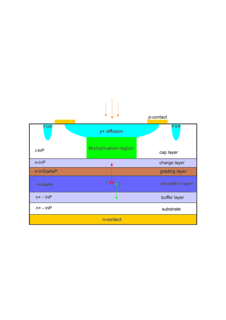
The typical heterojunction of InGaAs/InP SPADs are based on separate absorption, grading, charge, and multiplication (SAGCM) structure [5], as shown as Fig 1. With reverse bias, such structure can guarantee high electric field in the multiplication layer to enhance the avalanche probability while relatively low electric field in the absorption layer to reduce dark current due to tunneling effects [5]. Meanwhile, the grading layer is inserted between the absorption and multiplication layers to avoid the accumulation of trapped carriers during avalanche process so that the afterpulsing effect can be reduced, and the charge layer between the absorption and multiplication layers is to tailor the internal electric field profile [5].
Given an InGaAs/InP SPAD operated in Geiger mode, the reverse bias is above the breakdown voltage. In the absorption layer, an incoming photon may generate an electron-hole pair. Due to the electric field, the hole passes across the InGaAsP grading layer and the InP charge layer, and is finally drifted to the multiplication layer, in which a self-sustaining avalanche may be created. The avalanche is then sensed by a discriminator and quenched with a readout circuit by lowering the bias below the breakdown voltage.
The parameter of PDE [21] is defined as the probability of producing a correct output signal in response to an incident photon. Therefore, PDE of InGaAs/InP SPADs can be expressed by [4]
| (1) |
where is the coupling efficiency, is the absorption efficiency in the absorption layer, is the efficiency of photo-generated carriers injected from the absorption layer to the multiplication layer, and is the avalanche efficiency in the multiplication layer. For normal pigtailed SPAD devices, is a fixed value. Meanwhile, for SAGCM SPADs after an electron-hole pair is generated the effects of both the recombination in the absorption layer and the accumulation in the grading layer are negligible. In the simulation, and are supposed to be 1 for simplicity. can be calculated by
| (2) |
where is the absorption coefficient of In0.53Ga0.47As and is the absorption layer thickness.
is defined as the probability of creating a self-sustaining avalanche due to a hole entering into the multiplication layer, which highly depends on the electronic field or excess bias and temperature. In the model, the ionization coefficients of electron and hole are taken from the reference by Zappa et al. [22], which have been used to fit experimental results previously [12]. The electric field and temperature dependence of is then calculated using the model proposed by Oldham et al. [23], in which the dead space effect [24] have not been considered. As discussed in the references [25, 26], for SPADs with thick multiplication layers the dead space effect on carrier multiplication is negligible. Since the multiplication layer thickness of designed SPAD is normally larger than 1 m, using the model of Oldham et al. [23] to calculate is appropriate.
For the parameter of DCR [27], three generation mechanisms are considered [12], i.e., the thermal generation in the absorption layer, direct band-to-band tunneling and trap assisted tunneling (TAT) in the multiplication layer. The thermal generation induced DCR is primarily due to the Shockley-Read-Hall process and can be calculated as
| (3) |
where is the intrinsic carrier concentration and is effective lifetime of free carriers in the In0.53Ga0.47As layer. In the simulations, is assumed to be 50 s.
The direct band-to-band tunneling induced dark current density can be calculated as [12]
| (4) |
where is the bandgap of the multiplication layer, , and is the electric field. is the electric charge and is the reduced Planck constant. , where and are the effective masses of electrons and light holes, respectively.
During the process of TAT, a carrier is tunneled from the valence band to midgap between the conduction band and the valence band due to a defect, and the trapped carrier is then tunneled to the conduction band. TAT depends on the electric field, temperature, defect density and the activation energy of trapped state. The current density contribution of TAT can be calculated as [12]
| (5) |
where and are the densities of states in the valence and conduction bands, is the defect density in the multiplication layer, , , and and represent the energy barriers tunneling from the valence band to trap and tunneling from trap to the conduction band, respectively. and , in which is a fitting parameter [12]. In the model, and are assumed to be fixed as 0.75 and , respectively, for simplicity of simulations.
In the above model, the electric field distribution is a crucial parameter, which can be calculated using Gauss’s law given a reverse bias value. The SPAD parameters of breakdown voltage, and DCR highly depend on . Our simulation model is one-dimensional, and pre-mature edge-breakdown effect at the curved interface of the diffusion region has not been considered due to the fact that such effect can be well avoided by double diffusion process or float guard ring process [28]. Since our model is the same as that in Ref. [12], in which simulation results and experimental data agree with each other very well, we compare our simulation results of avalanche probability distribution with those in Ref. [12] given the same parameters. The exactly same results in two cases can well validate our simulation model.
3 Simulation results and discussion
In this section, we study the tradeoff between DCR and PDE under different conditions using the simulator, and then evaluate the performance in QKD applications. DCR and PDE are highly related to two structure variables, i.e., absorption layer thickness () and multiplication layer thickness (), and two operation variables as well, i.e., excess bias voltage () and temperature ().
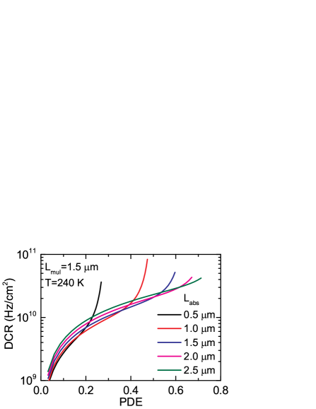
First, the variables of and are fixed whilst the variables of and vary, and the results are shown in Fig. 2. Linearly increasing corresponds to roughly linear increase of PDE and exponential increase of normalized DCR, so that DCR is an exponential function of PDE. When is low, the slope of exponential increase is moderate but becomes pretty steep in the region of high , as shown in Fig. 2. is chosen from 0.5 m to 2.5 m with a step of 0.5 m, and the maximum achievable PDE increases with an increase of .
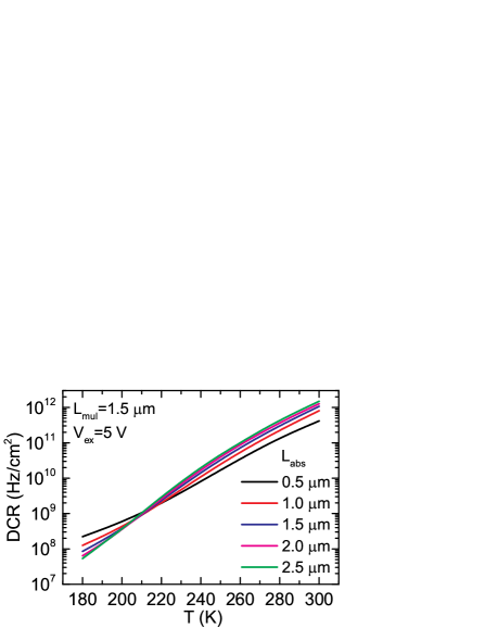
Second, we simulate the characteristic of temperature dependence. Fig. 3 shows DCR as a function of temperature in the cases of different absorption layer thicknesses, given fixed of 1.5 m and of 5 V. With a decrease of temperature, DCR decreases exponentially, and from Fig. 3 one can observe DCR reduction with 45 orders of magnitude when the temperature is cooled down from 300 K to 180 K. Such reduction is primarily due to the contribution of thermal generation, since thermal generation depends on from Eq. 3 and further decreases drastically with a decrease of temperature [29]. Moreover, one may find out an interesting phenomenon in Fig. 3, i.e., at temperatures higher than around 210 K larger induces higher DCR but this trend is reverse at temperatures below 210 K. This is probably due to the fact that thermal generation and TAT dominate DCR at high and low temperatures, respectively [5]. Under the conditions as shown in Fig. 3, 210 K may be the temperature turning point between the two DCR generation mechanisms.
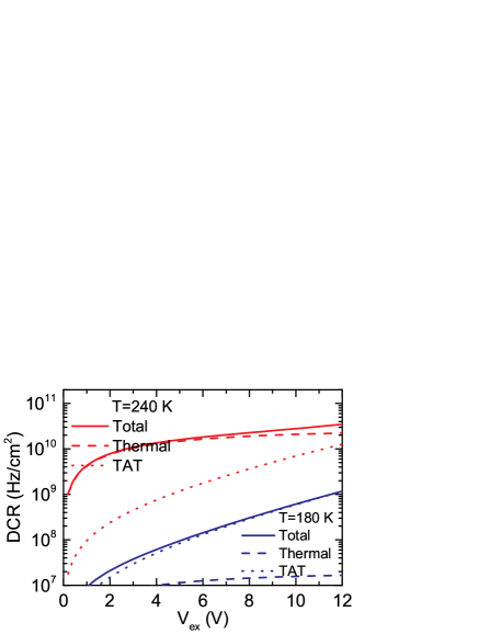
Third, to verify the contribution difference between the two DCR mechanisms, DCRs as a function of at two typical temperatures, i.e., 240 K in the high temperature region and 180 K in the low temperature region, are compared as shown in Fig. 4. Clearly, at 240 K thermal generation dominates DCR and the increase slope of DCR is flat particularly in the region of large . Similarly, at 180 K TAT dominates DCR and the increase slope of DCR becomes much steeper than that at 240 K.
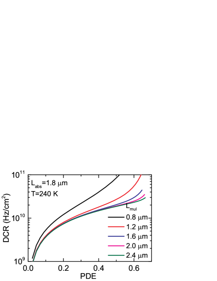
Finally, the variables of and are fixed whilst the variables of and vary. Fig. 5 exhibits DCR as a function of PDE with ranging from 0.8 m to 2.4 m. Given a PDE value, larger results in lower DCR performance. However, larger also induces worse timing jitter and higher afterpulse probability [3].
Therefore, to obtain good DCR and PDE performances the four variables have to be optimized. We propose an approach by evaluating the QKD performance to optimize SPAD parameters. In fiber-based QKD applications, the most important parameters are fiber distance and secure bit rate. Through QKD performance evaluation, one may globally optimize the structure and operation variables for SPADs. In the QKD simulations, decoy-state BB84 protocol [30, 31, 32, 33] using polarization encoding is used. The parameters and the corresponding values are listed in Table 1, some of which are taken from the reference [34]. Since the afterpulse probability () of SPAD is highly related with the quenching electronics [4], for simplicity it is assumed that the values of are fixed at 0.01 and 0.03 in the regions of low and high . For the SPADs used in the QKD simulations, the diameter of active area is set as 25 m, and the parameters of and are fixed at 1.8 m and 1.6 m, respectively.
| Parameter | Value |
|---|---|
| mean photon number of signal states () | 0.6 |
| mean photon number of decoy states () | 0.2 |
| probability ratio of the 3 intensities | 6:1:1 |
| repetition frequency () | 1 GHz |
| error correction factor () | 1.2 |
| optical fiber attenuation () | 0.2 dB/km |
| insertion loss in receiver () | 3 dB |
| error rate due to optical imperfections () | 0.01 |
| afterpulse probability of SPAD () | 0.01 (); |
| 0.03 () |
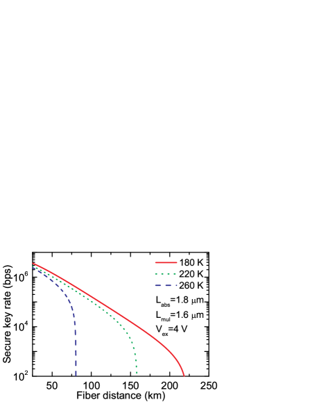
Given a fixed , the simulation results at different temperatures are shown in Fig. 6. In the region of short distances, the secure key rates are pretty high, and the key rate differences in three cases are small. Moreover, as temperatures decrease the maximum distances significantly increase. In the region of long distances, due to the low photon flux, DCR may dominate the quantum bit error rate so that DCR has to be greatly reduced in order to increase the secure key rate and distance. This also indicates that cooling down the SPAD temperature can be an effective method in order to further boost the maximum QKD distance, which has been experimentally demonstrated to achieve a record QKD distance of 307 km using an ultra-low noise InGaAs/InP SPAD [35].
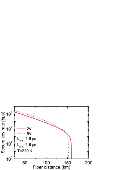
Similarly, Fig. 7 shows the simulations with different at the same temperature. Larger , corresponding to higher PDE, DCR and , has higher secure key rate and shorter maximum distance. Combining the results in Fig. 6 and Fig. 7, one can conclude that and temperature are the variables to be considered in prior for the aims of high key rate and long distance, respectively. Given a fixed QKD distance, through the optimization of and temperature the secure key rate can be maximized. Further, the variables of and can be optimized using better QKD performance as a reference, i.e., higher key rate and longer distance, under the conditions of the same and temperature.
4 CONCLUSIONS
In summary, we have modeled and developed an integrated simulation platform for InGaAs/InP SPADs. We focus on the intrinsic parameters of PDE and DCR, whose performance dependence on , , and temperature has been evaluated. To globally optimize the four variables for SPAD design and operations, the parameters of PDE and DCR are applied in the decoy-state QKD simulations, and the QKD performance is an important reference to determine the values of variables. This approach could be effective for designing high-performance InGaAs/InP SPADs in practice.
Acknowledgments
This work has been financially supported by the National Basic Research Program of China Grant No. 2013CB336800, the National Natural Science Foundation of China Grant No. 61275121, and the Chinese Academy of Sciences.
References
- [1] R. H. Hadfield, “Single-photon detectors for optical quantum information applications,” Nat. Photonics 3, 696 (2009).
- [2] M. D. Eisaman, J. Fan, A. Migdall, and S. V. Polyakov, “Invited review article: Single-photon sources and detectors,” Rev. Sci. Instrum. 82, 071101 (2011).
- [3] M. A. Itzler, X. Jiang, M. Entwistle, K. Slomkowski, A. Tosi, F. Acerbi, F. Zappa, and S. Cova, “Advances in InGaAsP-based avalanche diode single photon detectors,” J. Mod. Opt. 58, 174 (2011).
- [4] J. Zhang, M. A. Itzler, H. Zbinden, and J. W. Pan, “Advances in InGaAs/InP single-photon detector systems for quantum communication,” Light Sci. Appl. 4, e286 (2015).
- [5] M. A. Itzler, R. Ben-Michael, C.-F. Hsu, K. Slomkowski, A. Tosi, S. Cova, F. Zappa, and R. Ispasoiu, “Single photon avalanche diodes (SPADs) for 1.5 mm photon counting applications,” J. Mod. Opt. 54, 283 (2007).
- [6] S. Cova, M. Ghioni, A. Lacaita, C. Samori, and F. Zappa, “Avalanche photodiodes and quenching circuits for single-photon detection,” Appl. Opt. 35, 1956 (1996).
- [7] A. Lacaita, F. Zappa, S. Cova, and P. Lovati, “Single-photon detection beyond 1 m: performance of commercially available InGaAs/InP detectors,” Appl. Opt. 35, 2986 (1996).
- [8] G. Ribordy, J. Gautier, H. Zbinden, and N. Gisin, “Performance of InGaAs/InP avalanche photodiodes as gated-mode photon counters,” Appl. Opt. 37, 2272 (1998).
- [9] J. Rarity, T. Wall, K. Ridley, P. Owens, and P. Tapster, “Single-photon counting for the 1300-1600-nm range by use of Peltier-cooled and passively quenched InGaAs avalanche photodiodes,” Appl. Opt. 39, 6746 (2000).
- [10] P. Hiskett, G. Buller, A. Loudon, J. Smith, I. Gontijo, A. Walker, P. Townsend, and M. Robertson, “Performance and design of InGaAs/InP photodiodes for single-photon counting at 1.55 m,” Appl. Opt. 39, 6818 (2000).
- [11] S. Pellegrini, R. E. Warburton, L. J. Tan, J. S. Ng, A. B. Krysa, K. Groom, J. P. David, S. Cova, M. J. Robertson, and G. S. Buller, “Design and performance of an InGaAs/InP single-photon avalanche diode detector,” IEEE J. Quantum Electron. 42, 397 (2006).
- [12] J. P. Donnelly, E. K. Duerr, K. A. McIntosh, E. A. Dauler, D. C. Oakley, S. H. Groves, C. J. Vineis, L. J. Mahoney, K. M. Molvar, P. I. Hopman, K. E. Jensen, G. M. Smith, S. Verghese, and D. C. Shaver, “Design considerations for 1.06-m InGaAsP-InP Geiger-mode avalanche photodiodes,” IEEE J. Quantum Electron. 42, 797 (2006).
- [13] F. Acerbi, M. Anti, A. Tosi, and F. Zappa, “Design criteria for InGaAs/InP single-photon avalanche diode,” IEEE Photonics J. 5, 6800209 (2013).
- [14] X. Meng, C. Tan, S. Dimler, J. David, and J. Ng, “1550 nm InGaAs/InAlAs single photon avalanche diode at room temperature,” Opt. Express 22, 22608 (2014).
- [15] N. Namekata, S. Sasamori, and S. Inoue, “800 MHz Single-photon detection at 1550-nm using an InGaAs/InP avalanche photodiode operated with a sine wave gating,” Opt. Express 14, 10043 (2006).
- [16] Z. L. Yuan, B. E. Kardynal, A. W. Sharpe, and A. J. Shields, “High Speed Single Photon Detection in the Near Infrared,” Appl. Phys. Lett. 91, 041114 (2007).
- [17] J. Zhang, R. Thew, C. Barreiro, and H. Zbinden, “Practical fast gate rate InGaAs/InP single-photon avalanche photodiodes,” Appl. Phys. Lett. 95, 091103 (2009).
- [18] Y. Nambu, S. Takahashi, K. Yoshino, A. Tanaka, M. Fujiwara, M. Sasaki, A. Tajima, S. Yorozu, and A. Tomita, “Efficient and low-noise single-photon avalanche photodiode for 1.244-GHz clocked quantum key distribution,” Opt. Express 19, 20531 (2011).
- [19] X. L. Liang, J. H. Liu, Q. Wang, D. B. Du, J. Ma, G. Jin, Z. B. Chen, J. Zhang, and J. W. Pan, “Fully integrated InGaAs/InP single-photon detector module with gigahertz sine wave gating,” Rev. Sci. Instrum. 83, 083111 (2012).
- [20] A. Restelli, J. C. Bienfang, and A. L. Migdall, “Single-photon detection efficiency up to 50% at 1310 nm with an InGaAs/InP avalanche diode gated at 1.25 GHz,” Appl. Phys. Lett. 102, 141104 (2013).
- [21] D. A. Ramirez, M. M. Hayat, G. Karve, J. C. Campbell, S. N. Torres, B. E. A. Saleh, and M. C. Teich, “Detection efficiencies and generalized breakdown probabilities for nanosecond-gated near infrared single-photon avalanche photodiodes,” IEEE J. Quantum Electron. 42, 137 (2006).
- [22] F. Zappa, P. Lovati, and A. Lacaita, “Temperature dependence of electron and hole ionization coefficients in InP,” in Proc. IPRM 628 (1996).
- [23] W. G. Oldham, R. R. Samuelson, and P. Antognetti, “Triggering phenomena in avalanche diodes,” IEEE Trans. Electr. Dev. 19, 1056 (1972).
- [24] Y. Okuto and C. Crowell, “Energy-conservation considerations in the characterization of impact ionization in semiconductors,” Phys. Rev. B 6, 3076 (1972).
- [25] M. M. Hayat, B. E. A. Saleh, and M. C. Teich, “Effect of dead space on gain and noise of double-carrier-multiplication avalanche photodiodes,” IEEE Trans. Electr. Dev. 39, 546 (1992).
- [26] R. McIntyre, “A new look at impact ionization-part i: A theory of gain, noise, breakdown probability, and frequency response,” IEEE Trans. Electr. Dev. 46, 1623 (1999).
- [27] G. Karve, S. Wang, F. Ma, X. Li, J. C. Campbell, R. G. Ispasoiu, D. S. Bethune, W. P. Risk, G. S. Kinsey, J. C. Boisvert, T. D. Isshiki, and R. Sudharsanan, “Origin of dark counts in In0.53Ga0.47As/In0.52Al0.48As avalanche photodiodes operated in Geiger mode,” Appl. Phys. Lett. 86, 063505 (2005).
- [28] Y. Liu, S. R. Forrest, J. Hladky, M. J. Lange, G. H. Olsen, and D. E. Ackley, “A planar InP/InGaAs avalanche photodiode with floating guard ring and double diffused junction,” J. Lightw. Technol. 10, 182 (1992).
- [29] S. Paul, J. Roy, and P. Basu, “Empirical expressions for the alloy composition and temperature dependence of the band gap and intrinsic carrier density in GaxIn1-xAs,” J. Appl. Phys. 69, 827 (1991).
- [30] X.-B. Wang, “Beating the photon-number-splitting attack in practical quantum cryptography,” Phys. Rev. Lett. 94, 230503 (2005).
- [31] H.-K. Lo, X. Ma, and K. Chen, “Decoy state quantum key distribution,” Phys. Rev. Lett. 94, 230504 (2005).
- [32] X.-B. Wang, “Decoy-state protocol for quantum cryptography with four different intensities of coherent light,” Phys. Rev. A 72, 012322 (2005).
- [33] X. Ma, B. Qi, Y. Zhao, and H.-K. Lo, “Practical decoy state for quantum key distribution,” Phys. Rev. A 72, 012326 (2005).
- [34] Y. Liu, T.-Y. Chen, J. Wang, W.-Q. Cai, X. Wan, L.-K. Chen, J.-H. Wang, S.-B. Liu, H. Liang, L. Yang, C.-Z. Peng, K. Chen, Z.-B. Chen, and J.-W. Pan, “Decoy-state quantum key distribution with polarized photons over 200 km,” Opt. Express 18, 8587 (2010).
- [35] B. Korzh, C. C. W. Lim, R. Houlmann, N. Gisin, M. J. Li, D. Nolan, B. Sanguinetti, R. Thew, and H. Zbinden, “Provably secure and practical quantum key distribution over 307 km of optical fibre,” Nat. Photonics 9, 163 (2015).