Mapping the orbital structure of impurity bound states in a superconductor
Abstract
A magnetic atomic impurity inside a superconductor locally distorts superconductivity. They scatter Cooper pairs as a potential with broken time-reversal symmetry, what leads to localized bound states with subgap excitation energies, named hereon Shiba states. Most conventional approaches to study Shiba states treat magnetic impurities as point scatterers with an isotropic exchange interaction, while the complex internal structure of magnetic impurities is usually neglected. Here, we show that the number and the shape of Shiba states are correlated to the spin-polarized atomic orbitals of the impurity, hybridized with the superconducting host, as supported by Density Functional Theory simulations. Using high-resolution scanning tunneling spectroscopy, we spatially map the five Shiba excitations found on sub-surface chromium atoms in Pb(111), resolving both their particle and hole components. While the maps of particle components resemble the d orbitals of embedded Cr atoms, the hole components differ strongly from them. The orbital fingerprints of Shiba states thus unveil the magnetic ground state of the impurity, and identify scattering channels and interactions, all valuable tools for designing atomic-scale superconducting devices.
Yu-Shiba-Rusinov (Shiba) states Yu (1965); Shiba (1968); Rusinov (1969) are identified in scanning tunneling spectra as pairs of intra-gap resonances symmetrically positioned around zero-bias Yazdani et al. (1997); Hudson et al. (2001); Ji et al. (2008); Franke et al. (2011); Ruby et al. (2015a); Ménard et al. (2015). Each resonance is the excitation of an electron or hole into the bound state Ruby et al. (2015a), thus representing the particle or hole components of the quasiparticle wavefunction. Since Shiba excitations lie inside the superconducting gap, their lifetime considerably exceed that of other quasiparticles (QPs). This anticipates that Shiba peaks behave as a robust probe of scattering phenomena in superconductors, revealing intrinsic properties such as the distribution of the order parameter Hudson et al. (2001), the QP band structure McElroy et al. (2003), the effect of dimensionality Ménard et al. (2015), or Andreev tunneling processes Ruby et al. (2015a). Owing to their long lifetime, Shiba excitations exhibit narrow lineshapes, which enables the study of magnetic phenomena in impurities with high energy resolution, such as magnetic anisotropy Žitko et al. (2011); Hatter et al. (2015) and magnetic coupling Ji et al. (2008); Yao et al. (2014).

Theoretical models using classical spins with isotropic exchange fields have predicted multiple Shiba bound states associated to angular momentum quantum numbers Rusinov (1969). However, magnetic transition metal (TM) atoms in a superconductor show a varying number of Shiba bound states, that depends on the nature of both the element and the superconductor Pan et al. (2000); Hudson et al. (2001); Ji et al. (2008); Ruby et al. (2015a); Ménard et al. (2015). Due to the orbital character of the scattering channels of TM impurities, it is expected that Shiba multiplets reflect the occupation level of the atomic shell Moca et al. (2008), what would render them as the ideal probe for identifying the magnetic ground state of a single impurity in a superconductor. However, the orbital character of Shiba states remains elusive in the scarce previous attempts to experimentally map them Hudson et al. (2001); Ji et al. (2008); Ménard et al. (2015); Randeria et al. (2016), while their spatial extension has been mostly associated with the properties of the superconducting host.
Here we explore possible orbital components in Shiba states by comparing the QP local density of states (LDOS) of chromium atoms deposited on Pb(111), measured with a low temperature scanning tunneling microscope (STM), with atomistic simulations based on Density Functional Theory (DFT). We deposited Cr atoms on a Pb(111) film grown on SiC(0001) (thickness 100 nm) at 15 K. The atoms appear in STM images (measured at T = 1.2 K) as protrusions with a small apparent height of pm (Fig. 1 a) Ruby et al. (2015b), suggesting a subsurface atomic configuration of the Cr atoms. This is further supported by our DFT calculations (see Methods section and Supplementary Information (SI) for details), which reveal that the most stable configuration corresponds to the Cr atom underneath the uppermost Pb layer, as sketched in Figs. 1b and 1c.
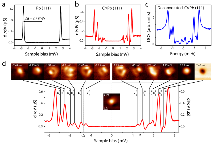
The quasiparticle LDOS associated to subsurface Cr impurities was obtained from differential tunneling conductance (dI/dV) spectra using superconducting Pb-terminated tips to increase the energy resolution beyond the thermal limit Franke et al. (2011). Figure 2a shows a typical dI/dV spectrum acquired on bare Pb(111) that exhibits a doubled SC gap of Pb with sharp coherence peaks at 2 meV not . The dI/dV curve taken on a Cr atom in Fig. 2b reveals a rich spectral structure inside the superconducting gap, with six intra-gap peaks at each polarity (i.e. six peak pairs), in addition to the original Pb coherence peaks. To obtain the quasiparticle LDOS, we deconvoluted the experimental dI/dV spectrum on chromium (Fig. 2b) using the superconducting DOS of a Pb-tip, estimated from Fig. 2a (details in SI SOM ). The deconvoluted spectrum, shown in Fig. 2c, shows just five energy-symmetric pairs of peaks, labeled as (n=1, 2, 3, 4, 5) in Fig. 2d. We attribute these pairs of peaks to five Shiba states with excitation energies meV, meV, meV, meV and meV. An additional pair of peaks, closest to zero bias in the dI/dV spectrum of Fig. 2b, denoted V and V, appear at bias voltages and, thus, corresponds to a thermal replica of the Shiba pair / Ruby et al. (2015a). Shiba multiplets arise naturally as different angular momentum components in isotropic exchange fields. However, the resolution of a five-fold Shiba multiplet achieved here enables us to reinterpret their origin in terms of atomic properties of the impurity Moca et al. (2008); Žitko et al. (2011).
To probe the orbital origin of the Shiba bound states, we map their intensity in a small region around the Cr impurity. Figure 2d shows dI/dV maps obtained for the same Cr atom at the voltages of all twelve peaks found inside the SC gap (See Methods). In contrast to the featureless protrusion in topography (inset of Fig. 2d), the conductance maps reveal various features around the Cr impurity. Each Shiba state appears with a different shape within the same polarity, as well as at the corresponding opposite polarity. For example, the shape of the QP states and , and are markedly different from their corresponding hole states, which reveals a particle-hole asymmetry in the wavefunction of the corresponding Shiba states. Such spatial asymmetry is also observed in the thermal replicas at and , which show the shapes of their mirror states and , respectively. The different shape of particle and hole components of every state explains their different peak amplitude in point spectra like in Fig. 2b. In fact, dI/dV spectra averaged over the whole extension around the Cr impurity levels their intensity at both polarities (see SI SOM ).
To find out the origin of the number and shape of the Shiba states, we simulated with DFT (see methods) the scattering channels of the embedded Cr impurity and modeled their effect in producing Shiba bound states. The channels are very sensitive to atomic-scale details of the Cr atom and its environment. We employed the most stable Cr site in the subsurface plane described in Figure 1b (see SI SOM ), and found that this site produced results compatible with the experiment.
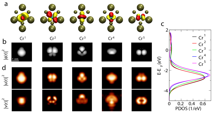
The identification of Cr-derived scattering channels is difficult; the embedded atom does not lie in a fully symmetric position inside the Pb FCC crystal, while it induces a significant displacement on its first Pb neighbors. Consequently, the Cr orbitals are strongly hybridized and mixed with Pb bands. To facilitate their identification in the band’s continuum, we calculated first the single-electron energy levels of the cluster formed by the Cr atom and the 7 first neighbours with apparent interaction (shown in Fig. 1c). We found that, at least in this reduced ensemble, there are five singly-occupied states with clear character centered in the Cr atom. Figure 3a plots isosurfaces of wavefunction amplitude for the five eigenstates inside the atomic cluster. Their shape partly resembles the original symmetry of orbitals. In the full Pb system, these states appear as broad resonances around -2.6 eV (Fig. 3c shows the DOS of the Pb slab projected on the five cluster states of Fig. 3a) due to the mixture with bands of the lead film, but their spin polarization remains very strong. We deem that these five one-electron states host the five spin-polarized scattering channels, through which the intra-gap bound states are created.
The spatial shapes of the five Cr-states of the cluster, projected on the surface (Fig. 3b), show already some level of agreement with the experimental Shiba maps. For example, the maps of peaks , , or resemble the shapes of states Cr3, Cr2, or Cr4, respectively. To correlate orbital states with subgap impurity bound states, we computed the corresponding Shiba states by considering that the effect of an impurity on the total Hamiltonian can be divided in potential (no spin degrees of freedom) and in spin contributions Rusinov (1969), such that
| (1) |
In a first approximation, the five scattering channels pictured in Fig. 3a diagonalizes these contributions. They are then responsible for the appearance of five positive-energy (particle) and five negative-energy (hole) Shiba states in the QP LDOS, symmetrically aligned with respect to the Fermi energy Moca et al. (2008). The DFT results indicate that for this system the potential scattering term in Eq. (1) is very small. In the absence of a potential scattering term, a large degree of particle-hole symmetry in the weight and amplitude of the Shiba states is expected Hudson et al. (2001); Flatté (2000). This is indeed the case after adding up all differential conductance spectra measured over the surface region around the Cr impurity, as commented above and shown in Fig. S3 in the SI SOM .
The spatial distribution of Shiba amplitudes can be depicted by the squared modulus of the Bogoliubov quasiparticle coefficients, and , representing the LDOS of their particle and hole components, respectively Fujita et al. (2008). Figure 3d plots the quantities and over the embedded Cr impurity, obtained as described in the SI SOM . The results reproduce the different shape of particle and hole states from the experiments: the particle component resembles the shape of Cr states in Fig. 3c, while deviates strongly. This is due to the dominating spin contribution to the potential: QP scattering with hole components produces a phase reversal for wavevectors of the Fermi surfaces of lead, resulting in a clear distortion of the shape of scattering channels SOM .
We can recognize several features from the experimental conductance maps of Shiba states (Fig. 2d) in the simulated particle and hole components of Bogoliubov quasiparticles (Fig. 3d). In particular, the particle components of orbitals Cr2 and Cr4 resemble the shape of positive bias Shiba maps and , respectively, whereas their fits well with the corresponding negative-bias maps, and . However, the opposite behaviour is found for the Shiba bound state : the shape of the particle component matches with the negative bias map. The reversal of bias polarity of particle and hole components is a fingerprint of a quantum phase transition driving a spin channel from a doublet into a Shiba singlet state. This occurs when the exchange coupling constant is large to induce the breaking of a Cooper pair Salkola et al. (1997); Franke et al. (2011); Hatter et al. (2015). In our case, this reveals that the given scattering channel is fully screened into a singlet state due to a larger exchange potential and, thus, does not contribute to the total atomic spin.
The sharp maps of Shiba states change shape rapidly between peaks, in barely less than 200 eV, a much greater accuracy than any other method of orbital imaging one-electron states, and in spite of the large degree of hybridization of the buried atom. This is ensured by the superconducting gap in the QP spectrum, which keeps Shiba states with long excitation lifetimes and decoupled from other QPs (except indirectly via thermal effects and/or via Andreev processes Ruby et al. (2015a)). Moreover, Shiba states are fairly unperturbed by the presence of close impurities. Our measurements, shown in the SI SOM , reveal that two impurities separated by only 4 surface lattice parameters (1.4 nm) display largely undisturbed Shiba conductance maps, what is attributed to the short localization length scale of Shiba states in three dimensions Rusinov (1969); Ménard et al. (2015). This suggests that coupling impurity-induced bound states together into extended magnetic structures Ji et al. (2008); Nadj-Perge et al. (2014); Ruby et al. (2015c) requires impurity separations well in the sub-nm range. In these structures, identification of the characteristic orbital symmetries of impurity bound states is thus a unique fingerprint to unveil their (channel-specific) magnetic ground state, their magnetic coupling to other nearby impurities, and to follow the formation of extended Shiba bands.
I Methods
I.1 STM measurements
The experiments were conducted in a commercial SPECS GmbH Low-Temperature (1.2 K) STM, under Ultra-High Vaccum conditions. Pb(111) films (thickness 100 nm) on SiC(0001) substrates show crystalline grains with diameters larger than 300 nm. To increase the energy resolution, the STM tip was repeatedly embedded in the Pb film until a superconducting tip was obtained. The full superconducting state of the tip was proved by performing STS spectra on bare Pb regions and showing that the two sharp coherence peaks appear at a distance close to 4, where =1.35 meV, as in Fig. 2a. Contrary to single-crystal measurements Ruby et al. (2015b) the spectra on bare Pb films never showed the characteristic double gap structure, probably due to the small film thickness compared to the Pb coherence length-scale. Cr atoms were deposited on the Pb(111) surface at a surface temperature of 15K. The spectra shown were obtained using a lock-in amplifier, with modulation =10 V at 938.5 Hz. The Shiba conductance maps were obtained from a matrix of 5252 dI/dV(V) spectra measured in a region of 4.8 nm2 over the Cr impurity. The corresponding topography images do not show any of the features observed in the Shiba maps (see inset of Fig. 2d). Analysis of STM and STS data was performed with the WsXm Horcas et al. (2007) and SpectraFox Rub software packages.
I.2 Theoretical details
Standard calculations using DFT were performed to reproduce the total energy and the electronic structure of different configurations of a Cr atom on Pb (111) (see SI SOM ). The calculations unequivocally predict a subsurface configuration under the surface bridge site, with considerably distortion of the surface Pb layer. A minimal Pb-Cr cluster is used to determine the local electronic structure near the Cr atom. Using the wavefunctions of this cluster, the Bogoliubov-de Gennes equations are approximated, in the presence of an exchange field, obtaining the equivalent of Rusinov’s equations using generalized scattering channels and a non-free-electron normal metal. The equations are further approximated to yield the spatial distribution of the Shiba states, as detailed in SI SOM .
Acknowledgements
We acknowledge fruitful discussions with Sebastian Bergeret, Katharina Franke, and Benjamin Heinrich. DJC acknowledges the European Union for support under the H2020-MSCA-IF-2014 Marie-Curie Individual Fellowship programme proposal number 654469. We acknowledge financial support from Spanish MINECO (Grants No. MAT2015-66888-C3-2-R and MAT2013-46593-C6-1-P) and Diputacion Foral de Gipuzkoa for grant N∘ 64/15.
References
- Yu (1965) L. Yu, Acta Physica Sinica 21, 75 (1965).
- Shiba (1968) H. Shiba, Progress of Theoretical Physics 40, 435 (1968).
- Rusinov (1969) A. I. Rusinov, Soviet Journal of Experimental and Theoretical Physics 29, 1101 (1969).
- Yazdani et al. (1997) A. Yazdani, B. A. Jones, C. P. Lutz, M. F. Crommie, and D. M. Eigler, Science 275, 1767 (1997).
- Hudson et al. (2001) E. W. Hudson, K. M. Lang, V. Madhavan, S. H. Pan, H. Eisaki, S. Uchida, and J. C. Davis, Nature 411, 920 (2001).
- Ji et al. (2008) S.-H. Ji, T. Zhang, Y.-S. Fu, X. Chen, X.-C. Ma, J. Li, W.-H. Duan, J.-F. Jia, and Q.-K. Xue, Phys. Rev. Lett. 100, 226801 (2008).
- Franke et al. (2011) K. J. Franke, G. Schulze, and J. I. Pascual, Science 332, 940 (2011).
- Ruby et al. (2015a) M. Ruby, F. Pientka, Y. Peng, F. von Oppen, B. W. Heinrich, and K. J. Franke, Phys. Rev. Lett. 115, 087001 (2015a).
- Ménard et al. (2015) G. C. Ménard, S. Guissart, C. Brun, S. Pons, V. S. Stolyarov, F. Debontridder, M. V. Leclerc, E. Janod, L. Cario, D. Roditchev, et al., Nature Physics pp. 1013–1016 (2015).
- McElroy et al. (2003) K. McElroy, R. W. Simmonds, J. E. Hoffman, D.-H. Lee, J. Orenstein, H. Eisaki, S. Uchida, and J. C. Davis, Nature 422, 592 (2003).
- Žitko et al. (2011) R. Žitko, O. Bodensiek, and T. Pruschke, Physical Review B 83, 30 (2011).
- Hatter et al. (2015) N. Hatter, B. W. Heinrich, M. Ruby, J. I. Pascual, and K. J. Franke, Nat. Commun. 6 (2015).
- Yao et al. (2014) N. Y. Yao, C. P. Moca, I. Weymann, J. D. Sau, M. D. Lukin, E. A. Demler, and G. Zaránd, Physical Review B 90, 1 (2014).
- Ruby et al. (2015b) M. Ruby, B. W. Heinrich, J. I. Pascual, and K. J. Franke, Phys. Rev. Lett. 114, 157001 (2015b).
- (15) See the Supplementary Online Information for details.
- Pan et al. (2000) S. Pan, E. Hudson, K. Lang, H. Eisaki, S. Uchida, and J. Davis, Nature 403, 746 (2000), ISSN 1476-4687.
- Moca et al. (2008) C. Moca, E. Demler, B. Jankó, and G. Zaránd, Physical Review B 77, 1 (2008).
- Randeria et al. (2016) M. T. Randeria, B. E. Feldman, I. K. Drozdov, and A. Yazdani, Physical Review B 93, 1 (2016).
- (19) Note that the spectrum does not show the double superconducting gap characteristic of Pb(111) Ruby et al. (2015b). The origin of this probably lies with the use of a Pb film rather than a single crystal, as in Ref. Ruby et al. (2015b).
- Flatté (2000) M. E. Flatté, Phys. Rev. B 61, R14920 (2000).
- Fujita et al. (2008) K. Fujita, I. Grigorenko, J. Lee, W. Wang, J. X. Zhu, J. C. Davis, H. Eisaki, S. Uchida, and A. V. Balatsky, Phys. Rev. B 78, 054510 (2008).
- Salkola et al. (1997) M. I. Salkola, A. V. Balatsky, and J. R. Schrieffer, Phys. Rev. B 55, 12648 (1997).
- Nadj-Perge et al. (2014) S. Nadj-Perge, I. K. Drozdov, J. Li, H. Chen, S. Jeon, J. Seo, A. H. MacDonald, B. A. Bernevig, and A. Yazdani, Science 346, 602 (2014).
- Ruby et al. (2015c) M. Ruby, F. Pientka, Y. Peng, F. von Oppen, B. W. Heinrich, and K. J. Franke, Phys. Rev. Lett. 115, 197204 (2015c).
- Horcas et al. (2007) I. Horcas et al., Rev. Sci. Instrum. 78, 013705 (2007).
- (26) Spectrafox, by M. Ruby, http://www.spectrafox.com/.