Theory of substrate-directed heat dissipation for single-layer graphene and other two-dimensional crystals
Abstract
We present a theory of the phononic thermal (Kapitza) resistance at the interface between graphene or another single-layer two-dimensional (2D) crystal (e.g. MoS2) and a flat substrate, based on a modified version of the cross-plane heat transfer model by Persson, Volokitin and Ueba [J. Phys.: Condens. Matter 23, 045009 (2011)]. We show how intrinsic flexural phonon damping is necessary for obtaining a finite Kapitza resistance and also generalize the theory to encased single-layer 2D crystals with a superstrate. We illustrate our model by computing the thermal boundary conductance (TBC) for bare and SiO2-encased single-layer graphene and MoS2 on a SiO2 substrate, using input parameters from first-principles calculation. The estimated room temperature TBC for bare (encased) graphene and MoS2 on SiO2 are () and () MWK-1m-2, respectively. The theory predicts the existence of a phonon frequency crossover point, below which the low-frequency flexural phonons in the bare 2D crystal do not dissipate energy efficiently to the substrate. We explain within the framework of our theory how the encasement of graphene with a top SiO2 layer introduces new low-frequency transmission channels which significantly reduce the graphene-substrate Kapitza resistance. We emphasize that the distinction between bare and encased 2D crystals must be made in the analysis of cross-plane heat dissipation to the substrate.
I Introduction
Single-layer two-dimensional (2D) crystals such as graphene and molybdenum disulphide (MoS2) have drawn much interest on account of their potential for applications in nanoelectronic, optoelectronic and thermoelectric technology Schwierz (2010); Wang et al. (2012); Ferrari et al. (2015). However, the integration of such materials into realistic device configurations requires them to be in physical contact with other commonly used CMOS (complementary metal-oxide-semiconductor) technology-compatible materials such as silicon dioxide (SiO2). Although the subnanometer thickness of such 2D crystals offers considerable advantage in electrostatic channel scaling in nanoelectronics Schwierz (2010); Liu et al. (2012); Lembke et al. (2015), the limited bulk volume is associated with high power densities and substantial waste Joule heat at high fields Meric et al. (2008); Serov et al. (2014), which, if not properly dissipated, increases operating temperatures and has a deleterious effect on device performance and lifetime Pop (2010). The waste heat can diffuse laterally within the 2D crystal and/or directly into the substrate on which the 2D crystal is supported Bae et al. (2010). In larger devices, heat dissipation to the substrate is the primary mechanism via which this waste heat is removed. The rate of heat dissipation depends on the intrinsic voluminal thermal resistance of the substrate material and the thermal (Kapitza) resistance of the interface between the 2D crystal and the substrate. Therefore, understanding the physical mechanism by which the 2D crystal thermally couples to the substrate is important for the technological development of 2D materials like graphene and semiconducting transition metal dichalcogenides. However, we lack a useful theoretical model of heat transfer between 2D crystals and the three-dimensional (3D) substrate because of their mismatch in dimensionality. In addition, there are several heat transfer processes (near-field radiative Volokitin and Persson (2011); Peng et al. (2015), electron-phonon Ong et al. (2013) and phononic Persson et al. (2011)) between the 2D crystal and the substrate which have been modeled analytically and numerically. The close agreement between experiments Chen et al. (2009); Mak et al. (2010) and molecular dynamics (MD) simulations of the thermal boundary conductance between graphene and different substrates suggests that heat is dissipated primarily through phonons (lattice vibrations) Ong and Pop (2011).
In spite of the considerable insight into the interfacial heat transfer process obtained from MD simulations, we still do not have a direct physical description of the phononic processes mediating heat dissipation from a single-layer 2D crystal to the substrate. For example, it is unclear what role the low-frequency phonons play in cross-plane heat dissipation. Furthermore, MD simulations are inherently classical in nature and cannot be related unambiguously to analysis involving quantum-mechanical phononic processes. Existing theories such as the acoustic mismatch model (AMM) and the diffuse mismatch model (DMM) employ analogies to acoustic scattering, specular or diffuse, to describe phonon transmission at the interface Swartz and Pohl (1989). However, the AMM and the DMM fundamentally assume that bulk incident phonons are transmitted across or reflected by the interface like acoustic or electromagnetic waves, a scenario that is not compatible with the geometrical configuration of supported single or few-layer 2D crystals where there is no extended volume in the direction normal to the interface. Therefore, it is necessary to formulate a fresh theory that takes into account the mismatch in dimensionality between the 2D crystal and its 3D substrate, and explicitly describes the phononic and vibrational character of such structures.
In our theory, we do not assume that the 2D crystal has any extended volume in the out-of-plane direction like in conventional mismatch models. Indeed, this approach offers us the unique advantage of directly linking the flexural nature of the 2D crystal to phonon transmission to the substrate. Moreover, this allows us to incorporate the effects of a superstrate, such as a top gate oxide layer, on heat dissipation to the substrate, and enables us to understand the difference in heat dissipation to the substrate by a bare 2D crystal and that by its encased counterpart. Our theory predicts that encased 2D crystals have a significantly higher thermal boundary conductance (or lower Kapitza resistance), consistent with empirical trends observed across different experiments. In spite of the simplicity of the model, its numerical predictions of the TBC are in very good agreement with published experimental data for graphene and MoS2, using numerical parameters obtained from first-principles calculations and published elasticity parameters.
The organization of our paper is as follows. We begin with the derivation of our theory of flexural phonon-mediated interfacial heat transfer for bare and encased graphene, and show how our theory is obtained by modifying the model by Persson, Volokitin and Ueba Persson et al. (2011). We then discuss how the damping function for flexural phonons, a key element of our theory, can be approximated and how the interfacial spring constant can be estimated in density functional theory (DFT) calculations. We apply the theory to estimate the TBC values for bare and SiO2-encased graphene and MoS2, and compare them with published experimental Freitag et al. (2009); Chen et al. (2009); Mak et al. (2010); Taube et al. (2015) and simulation Ni et al. (2013) data. Excellent agreement is obtained between our predicted TBC values and the various experimental and simulation data. We also discuss the physics underlying the higher TBC of SiO2-encased graphene and MoS2, and interpret it in terms of the additional low-frequency transmission channels due to coupling to the superstrate. Finally, we give an overall picture of the heat dissipation pathways in supported 2D crystals and discuss how the TBC may change when the different components are modified.
II Theory of heat transfer
II.1 Bare single-layer 2D crystal and solid substrate
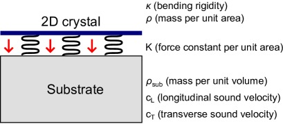
The point of departure in the formulation of our theory is Ref. Persson et al. (2011) by Persson, Volokitin and Ueba. We begin with a self-contained introduction to the essential elements of Ref. Persson et al. (2011), following closely the treatment in Ref. Persson et al. (2011). Suppose we have a single-layer 2D crystal supported by a flat substrate as shown in Fig. 1, with the -axis perpendicular to the substrate surface. The normal stress acting on the 2D crystal at position and time is
where and are respectively the out-of-plane displacement of the 2D crystal and the substrate surface, and is the spring constant per unit area characterizing the interaction, typically van der Waals, at the interface. If we take the Fourier transform of , i.e., where and are respectively the crystal momentum and frequency, then we have
| (1) |
The equation of motion for the 2D crystal is
| (2) |
where and are the mass density per unit area and the bending stiffness of the uncoupled 2D crystal, respectively and is the damping coefficient representing the intrinsic damping of the flexural motion. On the RHS of Eq. (2), represents the stochastic force from thermal fluctuation within the 2D crystal, in addition to the interface force from the substrate. The Fourier transform of Eq. (2) yields the algebraic expression
| (3) |
or
| (4) |
where
| (5) |
is the retarded Green’s function Amorim and Guinea (2013) for the flexural motion of the 2D crystal at the interface, and is the stochastic component of the flexural motion due to thermal fluctuation. Equation (4) describes the flexural response of the 2D crystal to a periodic harmonic stress exerted at the interface and the stochastic force. We modify Eq. (5) to take into account frequency-dependent damping by setting as a function of , i.e. . The key difference between our model and the one in Ref. Persson et al. (2011) is our inclusion of the damping process represented by the second term on the right hand side of Eq. (5). As we will show later, it allows us to avoid the weak coupling approximation in Ref. Persson et al. (2011) which can result in numerically inaccurate estimates of the Kapitza resistance. This damping term represents phenomenologically the coupling and exchange of energy between the flexural phonons with the other intrinsic degrees of freedom (e.g. electrons and in-plane acoustic phonons) in the 2D crystal. Physically, this means that a time-dependent applied force at the interface results in the excitation of flexural modes but the energy of these flexural phonons eventually dissipates to and is adsorbed by the other intrinsic degrees of freedom to which the flexural phonons are coupled. In the language of many-body physics, the damping term corresponds to the self-energy from the interaction of the flexural phonons with other intrinsic degrees of freedom.
The response of the substrate surface to the interfacial stress is similarly expressed as
| (6) |
where is the retarded Green’s function for the free surface displacement of the isotropic solid substrate. Within the elastic continuum model, for an elastic solid with isotropic elastic properties, we have Persson (2001); Persson et al. (2011)
| (7) |
where
| (8a) | |||
| (8b) | |||
| (8c) |
and , and are the longitudinal and transverse velocities, and the mass density per unit volume, respectively. Given the stochastic thermal fluctuation in the 2D crystal, the resultant motion of the 2D crystal and the substrate can be obtained by combining Eqs. (4) and (6) to yield:
| (9a) | |||
| (9b) |
Given the thermal fluctuation in the flexural motion of the 2D crystal, this stochastic motion also causes the interfacial stress on the substrate surface to fluctuate and transmit energy back and forth between the 2D crystal and the substrate. The associated thermal energy transfer from the 2D crystal to the substrate over the time period is
where the spatial integration is over the entire plane of the interface. One can also write
| (10) |
Substituting Eqs. (1) and (9b) in Eq. (10), we have the expression for the average thermal energy transfer, i.e.,
| (11) |
where denotes the thermal average. We can write as the Fourier transform of the autocorrelation function of the displacement , i.e.,
| (12) |
where
and is the area of the interface. The fluctuation-dissipation theorem Persson et al. (2011) implies that
| (13) |
where is the Bose-Einstein occupation function for frequency at temperature . The heat current from the 2D crystal to the substrate due to the thermal fluctuations in the 2D crystal is . Thus, Eq. (11) gives us the expression for the average power dissipated from the 2D crystal to the substrate:
Using the same procedure, a similar expression can be obtained for the average power dissipated from the substrate to 2D crystal, . Therefore, the thermal boundary conductance for the interface Persson et al. (2011) is , giving us
| (14) |
We can express Eq. (14) in the more familiar Landauer form
| (15) |
where
| (16) |
is the transmission function at . If we assume that and , we can show in Appendix A that which is exactly the property needed for a transmission coefficient.
Here, we comment on the weak coupling approximation originally used in Ref. Persson et al. (2011) for evaluating Eq. (14). It is claimed Persson et al. (2011) that the denominator in Eq. (16) can be ignored when the coupling between the two solids is weak (i.e., is so small that ) and that the numerator in Eq. (16) is thus dominated by the pole contribution from at the -point where the dispersion curves for the substrate Rayleigh modes and the bending modes of the 2D crystal intersect. However, this argument does not hold because the denominator diverges along the poles of and and there are actually no singularities in which is strictly less than or equal to unity (see Appendix A for the proof). Therefore, the weak-coupling approximation is incorrect and the denominator in Eqs. (16) and (14) must be retained to avoid spurious singularities. Our calculations of the integral [Eq. (14)] without the weak-coupling approximation indicate that the integral in Eq. (14) converges numerically to zero if there is no damping. This is because is only nonzero when along the poles of and when there is no damping, i.e. . Elsewhere, the numerator in the RHS of Eq. (16) and hence, are zero. Physically, this means that a dissipative mechanism must be present for net heat transfer to take place. This invalid approximation also explains why the numerical estimate Persson et al. (2011) of the TBC for the graphene/SiO2 interface is an order of magnitude too large.
II.2 Single-layer 2D crystal with superstrate and solid substrate
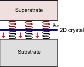
In more practical device designs, the perpendicular electrostatic field is applied through a top gate which consists of a metal insulated from the channel by a layer of oxide such as SiO2 or HfO2. Top-gated graphene and MoS2 field-effect transistors are known to have superior carrier density modulation and higher mobilities Fallahazad et al. (2010, 2012); Ong and Fischetti (2012, 2013a); Radisavljevic and Kis (2013); Ong and Fischetti (2013b) because of better charge screening. However, the effect of the top oxide layer, the superstrate, on heat dissipation from the encased 2D crystal to the substrate has not been systematically studied or even considered.
Given the theory of heat transfer between the bare 2D crystal and the substrate surface, it is possible incorporate the effects of a superstrate, as shown in Fig. 2, on the 2D crystal by modifying the equation of motion in Eq. (3). Let be the out-of-plane displacement of the bottom surface of the superstrate and , where is the spring constant per unit area characterizing the coupling to the superstrate, be the force per unit area exerted by the superstrate on the 2D crystal. Therefore, the equation of motion for the 2D crystal is
| (17) |
Like in Eq. (6), we define the surface response of the superstrate as
| (18) |
where is the retarded Green’s function for the free surface displacement of the superstrate. We combine Eqs. (17) and (18) to obtain the effective equation of motion for the 2D crystal analogous to Eq. (3)
| (19) |
where is the ‘self-energy’ contribution from coupling to the superstrate. Therefore, we define the effective retarded Green’s function for the flexural motion of the covered 2D crystal as
| (20) |
In the case of a top oxide layer, may have the same functional form as Eq. (7). In fact, if the superstrate is of the same material as the substrate, we can set and . For a thin film of adsorbates on the 2D crystal, we can write where is mass density of the adsorbates. In our simulations, we assume that the superstrate material is SiO2 like the substrate and the interfacial spring constant per unit area for the top and bottom interfaces of the 2D crystal are equal. Hence, like Eq. (14), the expression for the thermal boundary conductance is
| (21) |
III Additional details on numerical calculations
Although the details of our theory of heat transfer are described in Section II, there are two other important elements that are needed for the calculation of the thermal boundary conductance and warrant a more in-depth discussion before the theory can be made useful for numerical calculations. The first is the function form of the damping function for the flexural phonons while the second is the spring constant at the interface. The other material parameters such as the bending rigidity () and the 2D crystal mass density () can be obtained from literature.
III.1 Damping function for flexural phonons
A key element of our theory is the form of the damping function that determines the rate at which the flexural (ZA) phonon dissipates energy internally to other intrinsic degrees of freedom and is necessary to produce a finite Kapitza resistance. First principles calculations of the room-temperature anharmonic phonon-phonon scattering rate for long-wavelength flexural phonons in single-layer graphene by Bonini et al. Bonini et al. (2012) suggest that , i.e., the flexural phonon lifetime is proportional to its period. The same linear relationship between the scattering rate and the frequency of the long-wavelength flexural phonons is also observed in Ref. Lindsay et al. (2014). In this work, we ignore the effects of direct electron-phonon coupling on flexural phonon scattering since the interaction is a second-order effect Viljas and Heikkilä (2010); Castro et al. (2010); Mariani and von Oppen (2008) and the flexural phonon lifetimes in graphene can be satisfactorily explained Lindsay et al. (2010, 2014) without including the effects of flexural phonon scattering with electrons. Moreover, there is close agreement for the thermal conductivity in graphene between experimental data and theoretical estimates Lindsay et al. (2010, 2014) that are calculated using only anharmonic phonon coupling and without any electron-phonon interactions. Thus, the electron-phonon contribution to flexural phonon damping is small and can be neglected. Likewise, the thermal conductivity of MoS2 can also be modeled without needing to consider the effects of electron-phonon scattering on the acoustic phonon lifetimes Li et al. (2013); Wei et al. (2014).
Given that for a damped harmonic oscillator, we estimate from Ref. Bonini et al. (2012) that in graphene at room temperature ( K) although the ratio is slightly lower at in Ref. Lindsay et al. (2014). The quality factor in graphene nanoresonators has also been estimated to be around and to scale as in molecular dynamics simulations Jiang et al. (2014). Therefore, we propose a phenomenological expression for the temperature-dependent in graphene:
| (22) |
where is equal to the ratio of the phonon lifetime to its period at room temperature. In our simulations, we set to for single-layer graphene and MoS2. In the case of MoS2, there is less certainty over the value of as there is no readily available data on the relationship between flexural phonon lifetime and frequency although molecular dynamics simulations in Ref. Jiang et al. (2014) show that the quality factor for MoS2 is about three times that for graphene, suggesting that can be as high as . We note that in spite of the high flexural phonon lifetimes in MoS2, its thermal conductivity is much lower than that of graphene because of the low phonon group velocities in MoS2 and the stronger anharmonicity for the in-plane longitudinal and transverse acoustic phonons Li et al. (2013); Wei et al. (2014).
The functional form of Eq. (22) also means that flexural phonon damping increases linearly with temperature Klemens (1958). We stress that the functional form of Eq. (22) is approximate and that its frequency and temperature dependence can be in principle more precisely evaluated through DFT calculations and more sophisticated many-body techniques although this is beyond the scope of our current work. The damping is also expected to be higher when the graphene or MoS2 has intrinsic defects such as grain boundaries or vacancies that can reduce the flexural phonon lifetimes through elastic scattering.
III.2 Density functional theory calculation-based estimate of spring constant at interface
Another important parameter needed for our numerical calculation is , the spring constant per unit area for the interface. The numerical value of depends on the 2D crystal, the substrate and the surface atomistic structure of the substrate. We estimate the numerical values of from first principles calculations by computing the energy change when the 2D crystal is displaced from its equilibrium distance to the substrate surface. The change in energy per unit area for small displacements is thus
where is the energy change for the interface, is the area of the interface and is the distance between the 2D crystal and the substrate surface.
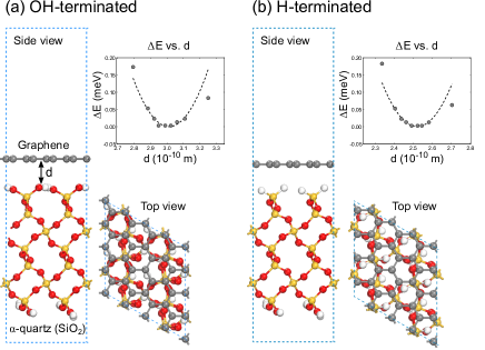
We estimate for graphene and MoS2 on H- and OH-terminated SiO2 from density functional theory (DFT) calculations. The interlayer spacing-energy () profiles for the various heterostructures (graphene/SiO2 and MoS2/SiO2) are calculated with the first-principles method within the framework of density functional theory by using the software package VASP Kresse and Furthmüller (1996). The DFT-D2 method is adopted to simulate the van der Waals interactions across the interface. The Perdew-Burke-Ernzerhof functional is used as the exchange-correlation functional together with a cutoff energy of 400 eV. The slab models are constructed with the vacuum layer thicker than 10 Å. For graphene/SiO2 (MoS2/SiO2), the heterostructures are constructed based on a () supercell for the graphene (MoS2) and a supercell for the SiO2 (001) surface for better lattice match with lattice strains smaller than 2 percent. For simulating the SiO2 (001) surface, a slab model with including seven Si layers is used and the atoms in the bottom O-Si-O atomic layers are saturated with hydrogen atoms and fixed during the structural optimization. Two types of surface of SiO2 with OH-rich and H-rich chemical conditions are considered for both graphene/SiO2 and MoS2/SiO2 heterostructures. We adopt a Monkhorst-Pack (MP) grid for k-point sampling for the graphene/SiO2 and graphene/MoS2 structures. All the atomic models are fully relaxed until the forces are smaller than 0.005 eV/Å.
Figure 3 shows the supercell of the graphene/SiO2 heterostructures used in our DFT calculations. The values for the graphene/SiO2 interface can be estimated by fitting the parabola around the minimum of the curve. We also estimate the values for the MoS2/SiO2 interface using the same procedure. The extracted values ( and ) are given in Table 1. We remark that the DFT-based estimated values of for the graphene/SiO2 interface are an order of magnitude than the value estimated by Cullen et al. Cullen et al. (2010) from graphene adhesion to SiO2 ( Nm-3). Given the sensitivity of the TBC to the numerical value of , the close agreement between our estimates of the graphene/SiO2 TBC and experimental data (see Table 2) suggests that the value of estimated in Ref. Cullen et al. (2010) is much too low.
| Graphene | MoS2 | |
|---|---|---|
| ( Nm-3) | ||
| ( Nm-3) | ||
| (eV) | Persson et al. (2011) | Jiang et al. (2013) |
| ( kgm-2) | ||
| (kgm-3) | Persson et al. (2011) | |
| (ms-1) | Persson et al. (2011) | |
| (ms-1) | Persson et al. (2011) | |
IV Results and discussion
We use our theory to calculate the Kapitza resistance for single-layer graphene and MoS2 on solid SiO2. The parameters in our simulations are given in Table 1. We evaluate the two-dimensional integral in Eq. (16) numerically with a rectangular grid in and . We set a frequency cutoff of meV which approximates the maximum flexural phonon energy at the Brillouin zone edge in most 2D materials. At low and room temperature, the numerical value of is relatively insensitive to the cutoff.
We note here that the following simulated TBC values are for an idealized flat interface at which the 2D crystal has full adhesion to the substrate or the superstrate in the case of the encased 2D crystal. The effective TBC values may be lower under most experimental conditions where some surface roughness is present, resulting in the reduction of the effective adhesion and contact area between the 2D crystal and the substrate Persson (2001); Persson et al. (2010); Persson and Ueba (2010); Persson et al. (2011). Thus, the simulated TBC values can be interpreted as the upper bounds for the TBC of real interfaces.
IV.1 Sensitivity of numerical results to damping friction
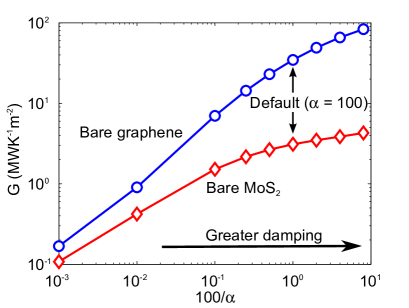
We calculate the room temperature ( K) thermal boundary conductance for bare graphene and MoS2 on OH-terminated SiO2 at different values of using Eq. (14) and the parameters from Table 1 except . Figure 4 shows the TBC as a function of . We find that as increases and the flexural phonon damping weakens, the TBC decreases and converges numerically to zero. The effect is more pronounced for graphene. This indicates that without any damping friction, the use of Eq. (14) yields an infinite Kapitza resistance. Physically, this means that damping friction in single-layer 2D crystals is necessary to produce a reasonable finite Kapitza resistance. It also confirms our earlier analysis of the weak-coupling approximation in Ref. Persson et al. (2011) which gives a TBC of MWK-1m-2, an order of magnitude larger than experimental data. In contrast, our default value of gives us a room-temperature TBC of MWK-1m-2 which is in very good agreement with published experimental data of bare single-layer graphene Mak et al. (2010); Freitag et al. (2009) ( MWK-1m-2) considering the uncertainty in the input parameters. We also observe that the TBC for MoS2 is considerably less sensitive to the numerical value of compared to graphene. When is quadrupled from to , the TBC decreases from MWK-1m-2 to MWK-1m-2. This considerably weaker -dependence in MoS2 implies that our choice of will not affect our TBC estimates for MoS2 significantly.
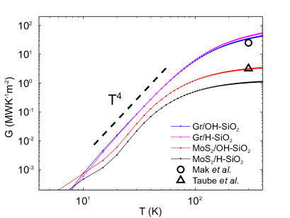
IV.2 Bare single-layer graphene and MoS2
We calculate the TBC for bare single-layer graphene and MoS2 on OH- and H-terminated SiO2 surface in the temperature range of 5-400 K using Eq. (14) and the parameters from Table 1. The computed results are shown in Fig. 5 along with the room-temperature experimental data for bare graphene and MoS2 from Refs. Mak et al. (2010) and Taube et al. (2015). At room temperature, the TBC values for graphene are relatively close regardless of the surface termination type (H or OH) although the H-terminated surface gives slightly higher TBC values. In contrast, the TBC values for MoS2 vary significantly at all temperature. At 300 K, we have and MWK-1m-2 for H- and OH-terminated SiO2 surfaces, respectively, indicating that bare MoS2 dissipates heat much more efficiently to the OH-terminated SiO2 surface than to the H-terminated surface. This is not surprising considering that is significantly higher than for MoS2 (see Table 1) because of the stronger coupling between MoS2 and OH-terminated SiO2. The simulated room-temperature TBC values are summarized in Table 2. At temperatures below 100 K, the TBC scales approximately as , assuming the temperature dependence of given in Eq. (22).
We compare our simulated TBC values with those measured from experiments on bare graphene or MoS2 on SiO2 at room temperature. By using an ultrafast optical pump pulse and monitoring the transient reflectivity on the picosecond time scale, Mak et al. Mak et al. (2010) obtained MWK-1m-2 for the room-temperature TBC of bare graphene on SiO2. A similar value is estimated by Freitag et al. in Ref. Freitag et al. (2009). Ni et al. Ni et al. (2013) obtained a value of MWK-1m-2 from their molecular dynamics (MD) simulations of single-layer graphene on amorphous SiO2 while Ong and Pop Ong and Pop (2010) obtained MWK-1m-2 from the MD simulation of a single-walled carbon nanotube on SiO2. These experimental and MD simulation values compare favorably with our estimate of 34.6 MWK-1m-2 for graphene on OH-terminated SiO2. For bare MoS2 on SiO2, a TBC value of MWK-1m-2 is estimated from Ref. Taube et al. (2015) using , where m2KW-1 is the thermal resistance of 275 nm of amorphous SiO2, with a thermal conductivity Regner et al. (2013) of MWK-1m-1, and m2KW-1 is the total interfacial thermal resistance measured using an optothermal method based on Raman spectroscopy Taube et al. (2015). This estimate is remarkably close to our calculated value of MWK-1m-2 for bare MoS2 on OH-terminated SiO2. For both graphene and MoS2 , given the good agreement between the simulated TBC values for OH-terminated SiO2 and experimental TBC data, this indirectly suggests that the spring constant per unit area for the OH-terminated surface is more representative of real SiO2 surface in experimental systems.
IV.3 Effect of top SiO2 layer on thermal boundary conductance
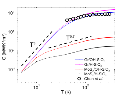
We calculate the TBC for SiO2-encased single-layer graphene and MoS2 on OH- and H-terminated SiO2 surface in the temperature range of 5-400 K using Eq. (21) and the parameters from Table 1. The computed results are shown in Fig. 6 along with the temperature-dependent experimental data for encased graphene from Refs. Chen et al. (2009) and the simulated room-temperature TBC values are given in Table 2. The TBC values are significantly higher for encased graphene and MoS2 than for the bare 2D crystals at all temperatures. In particular, the room-temperature TBC calculated for graphene on OH-terminated SiO2 is MWK-1m-2, in good agreement with the experimental values of MWK-1m-2 in Ref. Chen et al. (2009), and much larger than the corresponding TBC value for bare graphene. Like with our simulated TBC values for bare graphene, the computed values for the OH-terminated SiO2 interface is closer to experimental values. However, the TBC data from Ref. Chen et al. (2009) does not decrease as much with temperature as does our simulated data. This weaker temperature dependence may be due to the functional form of we assumed in Eq. (22). It is possible that a more accurate calculation of the temperature-dependent flexural phonon lifetime similar to what is done in DFT-based calculations of the thermal conductivity Bonini et al. (2012); Lindsay et al. (2014) will yield a TBC temperature dependence closer to experiments. In addition, the scaling may not hold at lower temperatures where defect scattering of the flexural phonons may be the limiting factor instead of anharmonic phonon interaction in real graphene. We also find that the TBC values for MoS2 vary significantly at all temperature with the surface termination type. At 300 K, we have and MWK-1m-2 for H- and OH-terminated SiO2 surfaces, respectively, indicating that encased MoS2 dissipates heat much more efficiently to the OH-terminated SiO2 surface than to the H-terminated surface like in bare MoS2. The temperature dependence of the TBC also varies with the 2D crystal. At temperatures below 100 K, the TBC scales approximately as for graphene and for MoS2.
| OH-SiO2 | H-SiO2 | Experimental | |
|---|---|---|---|
| Bare Graphene | Freitag et al. (2009); Mak et al. (2010) | ||
| Encased Graphene | Chen et al. (2009) | ||
| Bare MoS2 | Taube et al. (2015) | ||
| Encased MoS2 | – |
IV.4 Transmission analysis of bare and encased graphene
The question the arises as to why the thermal boundary conductance is much higher for encased 2D crystals than for their bare counterparts. The transmission function in Eqs. (14) and (21) is given by
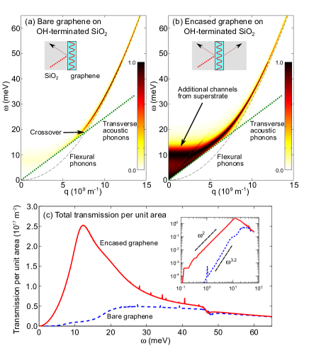
and its spectrum helps us to identify the dominant channels in heat dissipation. For an encased 2D crystal, we use instead of in . To illustrate the effect of the superstrate on heat dissipation, we plot the transmission spectra for bare and encased graphene on OH-terminated SiO2 in Fig. 7. Given that , the transmission spectrum for bare graphene [see Fig. 7(a)] is zero almost everywhere although the transmission peak is close to unity along the dispersion curve for the flexural phonons for meV, indicating the greater contribution from high-frequency modes. At lower frequencies ( meV), the transmission of individual low-frequency modes becomes rapidly more smeared out. In addition, the transmission is zero for since there are no substrate bulk acoustic phonon modes satisfying this condition, i.e., for . Physically, this means that heat dissipation can only take place when there is coupling to the substrate bulk acoustic phonons. Remarkably, the contribution of the low-frequency modes to interfacial heat transfer is relatively small for bare graphene. The crossover at meV is determined by the point where the graphene flexural phonon dispersion curve intersects the substrate transverse acoustic phonon dispersion curve, as can be seen in Fig. 7, and is given by . Below the crossover frequency, the substrate transverse acoustic phonons with the same wave vector have higher energy than the corresponding graphene flexural phonons. This reduces the probability of the flexural mode coupling with the continuum of substrate bulk phonons, which acts as a dissipative bath, and transferring energy into the substrate Amorim and Guinea (2013). Another way to understand this cutoff is that the region corresponds to substrate phonons with a transverse momentum component of and a frequency of , and these phonons scatter with graphene flexural phonons with the same and . We can also associate a characteristic length scale with the crossover point, given by nm where . This suggests that the TBC becomes strongly size-dependent when its interfacial area is comparable to or smaller than .
In contrast, Fig. 7(b) shows a very substantial low-frequency contribution in the transmissions spectrum of encased graphene, which also can be seen in Fig. 7(c) where we plot the total transmission per unit area . This is because the coupling of the 2D crystal to the superstrate results in the hybridization of the 2D crystal flexural modes with the superstrate Rayleigh modes Amorim and Guinea (2013); Ong and Pop (2011) and these superstrate/graphene hybrid modes can be scattered more easily into the substrate. The enhanced transmission of these low-frequency hybrid modes results in a significantly higher TBC for encased graphene. This difference in the low-frequency phonon contribution in the TBC of encased graphene also explains why the low-temperature scaling of is different in Figs. 5 and 6. At low frequencies, the total transmission per unit area scales as and in bare and encased graphene, respectively. The considerably weaker contribution of the low-frequency modes in bare graphene means that at lower temperatures, the higher-frequency modes do not contribute to interfacial heat transfer and the TBC decreases more rapidly as the temperature is reduced.
Physically, heat is exchanged between the SiO2 substrate and bare graphene when an incoming substrate bulk phonon scatters inelastically off the graphene/SiO2 interface and dissipates part of its energy within the graphene through the intrinsic flexural phonon damping, as represented schematically in the inset of Fig. 7(a). This scattering process efficiently dissipates energy from the substrate to the graphene when the substrate bulk phonon has a frequency (and hence energy) approximately equal to the corresponding graphene flexural phonon for the same . On the other hand, in encased graphene, the incoming substrate bulk phonon also scatters inelastically off the graphene/SiO2 interface and the energy is dissipated into the graphene. Part of the energy is absorbed by the intrinsic flexural phonon damping while part of it is absorbed by the flexural damping component from coupling to the superstrate. The latter can be interpreted as the partial transmission of energy into the bulk of the superstrate, as schematically represented in the inset of Fig. 7(b).
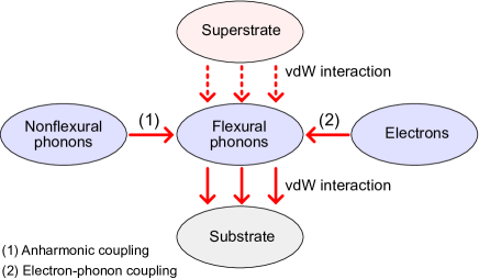
IV.5 Heat dissipation pathways
Our calculations of the thermal boundary conductance for bare and encased single-layer 2D crystals show that the presence of a superstrate on the 2D crystals can substantially increase the TBC between the 2D crystal and its substrate. In the bare 2D crystal, the energy from the intrinsic degrees of freedom (nonflexural phonons and electrons) are dissipated to the substrate via anharmonic or electron-phonon coupling to the flexural phonons. When a superstrate is placed on the 2D crystal, the flexural phonons are also mechanically coupled to the Rayleigh phonon modes from the superstrate. This mechanical coupling allows energy from the superstrate phonon modes, which we can consider as extrinsic degrees of freedom, to be dissipated to the substrate. Figure 8 shows a schematic representation of the different energy transfer pathways involved in heat dissipation to the substrate. In our simulations of bare and encased graphene and MoS2, we have used a phenomenological approach to describe the intrinsic anharmonic coupling to nonflexural phonons. In our study, we ignore dissipation via electron-phonon coupling because it is a second-order effect that involves two flexural phonons and two electrons Viljas and Heikkilä (2010); Castro et al. (2010); Mariani and von Oppen (2008) and is expected to be small although it may be significant at high electron temperatures and densities Song et al. (2012). Nevertheless, our estimates of the TBC with only dissipation from anharmonic phonon coupling are in excellent agreement with published experimental data, suggesting that the electron-phonon contribution is minor. Even so, it will be an interesting exercise to determine the TBC contribution from electron-phonon coupling at different electron temperatures and densities.
A slightly less intuitive consequence of our proposed theoretical framework for heat dissipation is that defect scattering of flexural phonons in the 2D crystal may increase the TBC. Here, we invoke the idea suggested by Song and Levitov Song et al. (2012) that a random distribution of short-range disorder can enlarge the scattering phase space for electron-phonon interactions by essentially lifting the momentum conservation restriction. Similarly, a random distribution of defects in graphene or MoS2 may enhance the effective anharmonic scattering rate of flexural phonons and increase the TBC. However, this method of enhancing the TBC may be counterproductive, especially in graphene, from the overall heat dissipation point of view since the flexural phonons are the dominant thermal transport carriers in graphene Seol et al. (2010); Lindsay et al. (2010) and the decrease of the flexural phonon lifetime will lower the thermal conductivity and reduce lateral heat dissipation.
V Summary and conclusions
We have modified the theory by Persson, Volokitin and Ueba Persson et al. (2011) and recast it in the Landauer form to study the Kapitza resistance of graphene and other single-layer 2D crystals on a solid substrate. We have shown that the weak-coupling approximation is not numerically valid and that the inclusion of a damping function for the flexural phonons is necessary to produce dissipation within the graphene and yield a finite Kapitza resistance. The phenomenological form of the damping function is deduced from published first-principles results. We have also shown how our theory can be modified to accommodate the effects of a superstrate. We have used DFT calculations to estimate the spring constant per unit area for the different interfaces. Our computed thermal boundary conductance values for bare single-layer graphene and MoS2 are in good agreement with published experimental data. The theory also suggests that there is no significant contribution to interfacial heat transfer by low-frequency phonon modes in bare single-layer 2D crystals.
We also find that the encasement of the 2D crystal by a SiO2 superstrate results in a increase in the thermal boundary conductance for graphene. This explains why the Kapitza resistance measured in experiments for SiO2-encased graphene is substantially lower than for bare graphene. This resistance reduction is also predicted to be true for single-layer MoS2. Our analysis shows that the increase in the thermal boundary conductance is due to the additional low-frequency transmission channels from coupling with the superstrate. We also find in bare 2D crystals that there is a crossover frequency below which phonons do not contribute significantly to cross-plane heat dissipation to the substrate. Our calculations suggest that the termination of the SiO2 surface has a much stronger influence on the Kapitza resistance for MoS2 than for graphene. The theoretical framework described in this work provides the basis for understanding how the modification of interfaces and 2D crystals at the nanoscale can be utilized to reduce the Kapitza resistance to improve interfacial heat dissipation, an important issue in the thermal management of nanoscale devices using 2D materials.
Acknowledgements.
This work was supported in part by a grant from the Science and Engineering Research Council (152-70-00017). We gratefully acknowledge the financial support from the Agency for Science, Technology and Research (A*STAR), Singapore and the use of computing resources at the A*STAR Computational Resource Centre, Singapore. We also acknowledge discussions with Eric Pop (Stanford University) and Justin Song (Institute of High Performance Computing).Appendix A Numerical bounds for transmission function
Let us write and where and are real numbers for . Thus, the transmission function in Eq. (16) can be written as
Given that , this means that
and therefore, we have .
References
- Schwierz (2010) F. Schwierz, Nature Nanotechnology 5, 487 (2010).
- Wang et al. (2012) Q. H. Wang, K. Kalantar-Zadeh, A. Kis, J. N. Coleman, and M. S. Strano, Nature Nanotechnology 7, 699 (2012).
- Ferrari et al. (2015) A. C. Ferrari, F. Bonaccorso, V. Fal’Ko, K. S. Novoselov, S. Roche, P. Bøggild, S. Borini, F. H. Koppens, V. Palermo, N. Pugno, et al., Nanoscale 7, 4598 (2015).
- Liu et al. (2012) H. Liu, A. T. Neal, and P. D. Ye, ACS Nano 6, 8563 (2012).
- Lembke et al. (2015) D. Lembke, S. Bertolazzi, and A. Kis, Accounts of Chemical Research 48, 100 (2015).
- Meric et al. (2008) I. Meric, M. Y. Han, A. F. Young, B. Ozyilmaz, P. Kim, and K. L. Shepard, Nature Nanotechnology 3, 654 (2008).
- Serov et al. (2014) A. Y. Serov, Z.-Y. Ong, M. V. Fischetti, and E. Pop, J. Appl. Phys. 116, 034507 (2014).
- Pop (2010) E. Pop, Nano Research 3, 147 (2010).
- Bae et al. (2010) M.-H. Bae, Z.-Y. Ong, D. Estrada, and E. Pop, Nano Lett. 10, 4787 (2010).
- Volokitin and Persson (2011) A. Volokitin and B. Persson, Phys. Rev. B 83, 241407 (2011).
- Peng et al. (2015) J. Peng, G. Zhang, and B. Li, Appl. Phys. Lett. 107, 133108 (2015).
- Ong et al. (2013) Z.-Y. Ong, M. V. Fischetti, A. Y. Serov, and E. Pop, Phys. Rev. B 87, 195404 (2013).
- Persson et al. (2011) B. N. J. Persson, A. I. Volokitin, and H. Ueba, J. Phys.: Condens. Matter 23, 045009 (2011).
- Chen et al. (2009) Z. Chen, W. Jang, W. Bao, C. N. Lau, and C. Dames, Appl. Phys. Lett. 95, 161910 (2009).
- Mak et al. (2010) K. F. Mak, C. H. Lui, and T. F. Heinz, Appl. Phys. Lett. 97, 221904 (2010).
- Ong and Pop (2011) Z.-Y. Ong and E. Pop, Phys. Rev. B 84, 075471 (2011).
- Swartz and Pohl (1989) E. T. Swartz and R. O. Pohl, Rev. Mod. Phys. 61, 605 (1989).
- Freitag et al. (2009) M. Freitag, M. Steiner, Y. Martin, V. Perebeinos, Z. Chen, J. C. Tsang, and P. Avouris, Nano Lett. 9, 1883 (2009).
- Taube et al. (2015) A. Taube, J. Judek, A. Lapinska, and M. Zdrojek, Appl. Mater. Interfaces 7, 5061 (2015).
- Ni et al. (2013) Y. Ni, Y. Chalopin, and S. Volz, Appl. Phys. Lett. 103, 141905 (2013).
- Amorim and Guinea (2013) B. Amorim and F. Guinea, Phys. Rev. B 88, 115418 (2013).
- Persson (2001) B. N. J. Persson, J. Chem. Phys. 115, 3840 (2001).
- Fallahazad et al. (2010) B. Fallahazad, S. Kim, L. Colombo, and E. Tutuc, Appl. Phys. Lett. 97, 123105 (2010).
- Fallahazad et al. (2012) B. Fallahazad, K. Lee, G. Lian, S. Kim, C. Corbet, D. Ferrer, L. Colombo, and E. Tutuc, Appl. Phys. Lett. 100, 093112 (2012).
- Ong and Fischetti (2012) Z.-Y. Ong and M. V. Fischetti, Phys. Rev. B 86, 121409 (2012).
- Ong and Fischetti (2013a) Z.-Y. Ong and M. V. Fischetti, Appl. Phys. Lett. 102, 183506 (2013a).
- Radisavljevic and Kis (2013) B. Radisavljevic and A. Kis, Nature Materials 12, 815 (2013).
- Ong and Fischetti (2013b) Z.-Y. Ong and M. V. Fischetti, Phys. Rev. B 88, 165316 (2013b).
- Bonini et al. (2012) N. Bonini, J. Garg, and N. Marzari, Nano Lett. 12, 2673 (2012).
- Lindsay et al. (2014) L. Lindsay, W. Li, J. Carrete, N. Mingo, D. A. Broido, and T. L. Reinecke, Phys. Rev. B 89, 155426 (2014).
- Viljas and Heikkilä (2010) J. K. Viljas and T. T. Heikkilä, Phys. Rev. B 81, 245404 (2010).
- Castro et al. (2010) E. V. Castro, H. Ochoa, M. I. Katsnelson, R. V. Gorbachev, D. C. Elias, K. S. Novoselov, A. K. Geim, and F. Guinea, Phys. Rev. Lett. 105, 266601 (2010).
- Mariani and von Oppen (2008) E. Mariani and F. von Oppen, Phys. Rev. Lett. 100, 076801 (2008).
- Lindsay et al. (2010) L. Lindsay, D. A. Broido, and N. Mingo, Phys. Rev. B 82, 115427 (2010).
- Li et al. (2013) W. Li, J. Carrete, and N. Mingo, Appl. Phys. Lett. 103, 253103 (2013).
- Wei et al. (2014) X. Wei, Y. Wang, Y. Shen, G. Xie, H. Xiao, J. Zhong, and G. Zhang, Appl. Phys. Lett. 105, 103902 (2014).
- Jiang et al. (2014) J.-W. Jiang, H. S. Park, and T. Rabczuk, Nanoscale 6, 3618 (2014).
- Klemens (1958) P. G. Klemens, in Solid State Physics, Vol. 7, edited by F. Seitz and D. Turnbull (Academic Press, 1958) pp. 1–98.
- Kresse and Furthmüller (1996) G. Kresse and J. Furthmüller, Phys. Rev. B 54, 11169 (1996).
- Cullen et al. (2010) W. G. Cullen, M. Yamamoto, K. M. Burson, J. H. Chen, C. Jang, L. Li, M. S. Fuhrer, and E. D. Williams, Phys. Rev. Lett. 105, 215504 (2010).
- Jiang et al. (2013) J.-W. Jiang, Z. Qi, H. S. Park, and T. Rabczuk, Nanotechnology 24, 435705 (2013).
- Persson et al. (2010) B. Persson, B. Lorenz, and A. Volokitin, Eur. Phys. J. E 31, 3 (2010).
- Persson and Ueba (2010) B. Persson and H. Ueba, J. Phys.: Condens. Matter 22, 462201 (2010).
- Ong and Pop (2010) Z.-Y. Ong and E. Pop, Phys. Rev. B 81, 155408 (2010).
- Regner et al. (2013) K. T. Regner, D. P. Sellan, Z. Su, C. H. Amon, A. J. H. McGaughey, and J. A. Malen, Nature Commun. 4, 1640 (2013).
- Song et al. (2012) J. C. W. Song, M. Y. Reizer, and L. S. Levitov, Phys. Rev. Lett. 109, 106602 (2012).
- Seol et al. (2010) J. H. Seol, I. Jo, A. L. Moore, L. Lindsay, Z. H. Aitken, M. T. Pettes, X. Li, Z. Yao, R. Huang, D. Broido, et al., Science 328, 213 (2010).