Microwave Admittance of Gold-Palladium Nanowires with Proximity-Induced Superconductivity
Abstract
We report quantitative electrical admittance measurements of diffusive superconductor–normal-metal–superconductor (SNS) junctions at gigahertz frequencies and millikelvin temperatures. The gold-palladium-based SNS junctions are arranged into a chain of superconducting quantum interference devices. The chain is coupled strongly to a multimode microwave resonator with a mode spacing of approximately . By measuring the resonance frequencies and quality factors of the resonator modes, we extract the dissipative and reactive parts of the admittance of the chain. We compare the phase and temperature dependence of the admittance near to theory based on the time-dependent Usadel equations. This comparison allows us to identify important discrepancies between theory and experiment that are not resolved by including inelastic scattering or elastic spin-flip scattering in the theory.
I Introduction
The transport of direct current (dc) between two superconductors (S) separated by a diffusive normal-metal (N) link is in general well understood both theoretically and experimentally.Clarke (1968); Usadel (1970); Likharev (1979); Dubos et al. (2001a); Heikkilä et al. (2002); Courtois et al. (2008) At low temperatures and currents, Andreev reflection Andreev (1965) leads to the formation of a gap in the density of quasiparticle states in N and allows a dissipationless supercurrent to flow. This gap has been directly observed in tunnel spectroscopy measurements.Guéron et al. (1996); le Sueur et al. (2008) Shapiro steps, supercurrent enhancement, and other non-equilibrium effects under intense microwave irradiation have also been extensively studied.Clarke (1968); Notarys et al. (1973); Warlaumont et al. (1979); Lehnert et al. (1999); Dubos et al. (2001b); Fuechsle et al. (2009); Chiodi et al. (2009); Virtanen et al. (2010)
In contrast, the near-equilibrium response of superconductor–normal-metal–superconductor (SNS) junctions to weak microwave radiation has become an active area of investigation only recently.Galaktionov and Zaikin (2010); Virtanen et al. (2011); Kos et al. (2013); Ferrier et al. (2013); Tikhonov and Feigel’man (2015) While the adiabatic contribution to the kinetic inductance can be calculated from the dc current–phase relation, at high frequencies both reactive and dissipative contributions also arise from other mechanisms, such as driven transitions between quasiparticle states and oscillation of the Andreev level populations.Virtanen et al. (2011) Surprisingly however, little experimental data has been published on the topic thus far.Chiodi et al. (2011); Dassonneville et al. (2013) The parameter regimes and materials studied in the published experiments are very sparse, hence limiting the extent to which theoretical predictionsGalaktionov and Zaikin (2010); Virtanen et al. (2011); Kos et al. (2013); Ferrier et al. (2013); Tikhonov and Feigel’man (2015) can be tested. In practice, data on the effective inductance and losses also expedites the process of designing high-frequency SNS-junction-based circuits, such as the SNS nanobolometer.Govenius et al. (2014, 2016)
Previous experimental studiesChiodi et al. (2011); Dassonneville et al. (2013) have probed flux- and temperature-dependent changes in the linear microwave response of a superconducting ring with a gold normal-metal inclusion. The superconducting ring consisted of ion-beam-deposited tungsten in the first experiments,Chiodi et al. (2011) and sputter-deposited Nb with a thin Pd layer at the SN interface in the later experiments.Dassonneville et al. (2013) A single SNS ring was biased with a dc magnetic flux and coupled weakly to a multi-mode microwave resonator. By measuring flux-dependent shifts in the quality factors and resonance frequencies, the authors determined how the complex-valued electrical susceptibility changes.Chiodi et al. (2011); Dassonneville et al. (2013) The change in , as a function of flux and temperature, was reported to be in excellent agreement with theoretical predictions based on Usadel equations and numerical simulations. However, the implicit offsets in both the real and imaginary parts of the reported susceptibility prevent a comparison to the theoretically predicted absolute values of and . They also prevent the accurate prediction of the effective inductance () and the loss tangent (), which are the key quantities for any practical high-frequency application of SNS junctions.
In this article, we present measurements of the SNS junction admittance for gold-palladium based junctions at angular frequencies of order . We use a chain of SNS superconducting quantum interference devices (SQUIDs) with a strong capacitive coupling to a multimode microwave resonator with a typical mode spacing of . Each chain consists of 20 SNS SQUIDs in series. The strong coupling and the large number of SQUIDs lead to significant changes in the frequencies and quality factors of the resonator modes, which allow determining without an offset. The absence of an offset enables us to show that the Usadel-equation-based theory we consider cannot simultaneously explain the observed real and imaginary parts of .
II Samples
We study the linear electrical response of SNS junctions at millikelvin temperatures in two samples: Sample 1 and 2. The gold-palladium nanowires used as the normal-metal are deposited simultaneously in the same fabrication steps as for our recent nanobolometer circuits.Govenius et al. (2016) We determine the Au:Pd atomic ratio of the alloy to be approximately 3:2 using energy-dispersive X-ray spectroscopy (see Section VII.1.3). The nominal junction length is and the nominal cross-sectional area is . The normal-state resistance of a single junction is estimated based on four-wire dc measurements of reference samples. From the reference measurements, we also estimate the upper bound for the contact resistance to be approximately . We only give an upper bound for the contact resistance because of the uncertainties introduced by the crossed-wire geometryPomeroy and Grube (2009) of the reference samples. Reference samples are similar to those in Figure 1b in Reference 25.
The key parameter determining the strength of the proximity-induced superconductivity is the Thouless energy , where is the diffusion constant. In our samples, the Thouless energy is , where and is the Boltzmann constant. The superconducting sections are 100-nm thick aluminum, which implies that the energy gap in the superconductors is much larger than the Thouless energy (). Both S and N parts are fabricated using electron beam lithography and evaporation. Further fabrication details are reported in the Experimental Section VII.1.
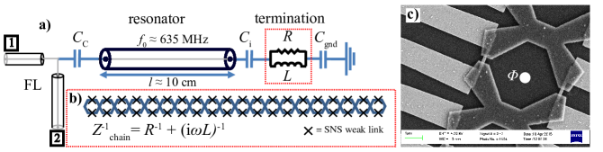
The SNS junctions are arranged into a chain of SQUIDs, as shown in Figure 1. Each SQUID loop has a relatively small area of in order to minimize sensitivity to external magnetic field noise. In addition, we measured Sample 2 in a double layer magnetic shield. The geometric inductance of each loop is small ( pH) compared to the effective inductance of the SQUID, as verified by the results below. A dc magnetic flux bias is applied by an external coil that provides a uniform flux bias for each SQUID in the 100 m long chain. Assuming identical junctions, this phase biases each SNS junction to at dc, where is the magnetic flux quantum and is the integer that minimizes . We note that the flux bias we label as may be offset from the true zero flux condition by an integer multiple of .
The SQUID chains in the two samples are nominally identical, except for the addition of heat sinks to Sample 2 (see Figure 1c). The heat sinks are designed to reduce the hot-electron effect,Wellstood et al. (1994) i.e., the increase of the quasiparticle temperature above the phonon bath temperature that we measure. For each SNS junction, the heat sink consist of two large () reservoirs of gold-palladium that are thermally strongly coupled to the junction.
In addition to the SQUID chain, the chip contains a transmission line resonator (see Figure 1a and Table 1). We characterize it by measuring control samples with an open termination, i.e., samples without the SQUID chain. From the control measurements, we extract the fundamental frequency of the transmission line resonator , and confirm that the internal quality factor for the resonances we consider (). The latter implies that we can neglect the losses in the transmission line part of the resonator, and in the Al2O3 used as the dielectric material in the lumped element capacitors (). This is valid because introducing the SQUID chain lowers to the order of , as observed below. We also deduce the characteristic impedance of the transmission line from the measured , the length of the resonator, and the design value for the inductance per unit length.
| Sample | (pF) | (pF) | (mm) | (MHz) | () | Heat sinks | |
|---|---|---|---|---|---|---|---|
| 1 | 0.15 | 14.5 | 97.2 | 637 | 39 | No | |
| 2 | 0.44 | 15.2 | 96.5 | 633 | 39 | Yes |
III Measurement scheme and sample characterization
We determine the admittance of the SQUID chain by embedding it as the termination of a long (10 cm) transmission line microwave resonator, as illustrated in Figure 1a. We first determine the resonance frequency and the internal quality factor of each mode by measuring the frequency-dependent transmission coefficient through the feedline. By comparing and to values measured in control samples, we can determine the admittance of the SQUID chain at multiple frequencies. Specifically, we use a circuit model (Figure 1a) that allows extracting the admittance of the SQUID chain from the response of the combined resonator/SQUID-chain system. The admittance of each individual SNS junction is then given by , assuming that the junctions are identical and that geometric inductance is negligible.
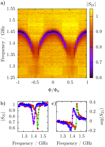
Figure 2 shows the normalized transmission through the feedline at frequencies near , probing the third () mode in Sample 2. The normalization (defined precisely in Section VII.3) removes all spurious features in the transmission data that do not depend on flux. What remains is the oscillatory flux dependence of the resonance frequency with a period we identify as . As the flux bias is increased away from integer multiples of , we measure a decrease in both the resonance frequency and the loaded quality factor . This behavior is more clearly visible in Figure 2b,c with individual slices of transmission data for and . These changes in the resonance indicate that both the inductance and the losses increase in the SQUID chain near half-integer values of .
To extract and quantitatively, we fit the measured normalized transmission for the mode to the model
| (1) |
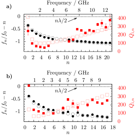
where is a fit parameter that characterizes asymmetry, and the external quality factor is governed by the coupling () to the feedline.Geerlings et al. (2012); Khalil et al. (2012) From the obtained fit parameters and , we compute the contribution of losses due to the SQUID chain as . Figure 3 shows the extracted values of and for frequencies up to ().
In the low-frequency and low-temperature regime, the SQUID chain behaves like an inductor, i.e., most of the admittance is reactive () and varies slowly as a function of the angular frequency . Consequently, we parametrize the admittance as a parallel combination of a resistor and an inductor, such that . Figure 3 demonstrates that this is a good parametrization by showing qualitative agreement between the experimental data and predictions for the mode shifts and quality factors using a simplified model where and are constant.
Let us now discuss the extraction of the admittance from the measured and values. For an ideal transmission line resonator with open-circuit conditions at both ends (), the mode is located at frequency . In contrast, for the samples with the SQUID chains, the frequency-dependent reactive, i.e., imaginary parts of the termination admittances and lead to the non-zero modeshift of Figure 3, that we use to determine . Similarly, the measured gives information about the dissipative, i.e., real part of .
Quantitatively, we determine the SQUID chain admittance from and by numerically solving the trancendental equation
| (2) |
using the parameters given in Table 1. We derive this equation from the circuit model shown in Figure 1, assuming that is dominated by losses in the SQUID chain.
Table 2 shows the and extracted for two examples resonances near 1 GHz. The reported values provide an important reference for designing high-frequency devices based on gold-palladium SNS junctions. That is, they imply that an effective inductance of a few hundred picohenries per junction and a loss tangent of a few percent can be expected around 1 GHz at millikelvin temperatures.
| Sample | (GHz) | () | (nH) | |||
|---|---|---|---|---|---|---|
| 1 | 0.914 | |||||
| 2 | 1.452 |
IV Theory
In the next section, we compare the experimental results to theoretical predictions Virtanen et al. (2011) based on the time-dependent Usadel equation.Usadel (1970) In the low-frequency and low-temperature regime considered below, the imaginary part of the admittance of the junction is expected to be mostly determined by the adiabatic Josephson inductance associated with the supercurrent, i.e., the derivative of the dc supercurrent. The real part, on the other hand, mainly arises from driven quasiparticle transitions in the junction. The availability of such transitions is sensitive to the density of quasiparticle states. In particular, the presence of a proximity-induced energy gap in the density of states should lead to an exponential increase in the resistance as decreases below .
However, the low-temperature values of and we measure (Table 2) are dramatically larger than those predicted using the parameters considered in Reference 18. This is evident from a cursory comparison of Figure 1 in Reference 18 to our and . The inductance per junction is also an order of magnitude higher than the expected adiabatic Josephson inductance , where we approximate the dc supercurrent as and the critical current as the ideal value for . Dubos et al. (2001a) Moreover—in the results below—we observe a weak temperature dependence of measured near 1 GHz, which is in stark contrast to the theoretically predicted exponential dependence.
The observed values of and imply that the the proximity-induced superconductivity is significantly weaker than expected. We consider two distinct scattering mechanisms as potential explanations for this. First, we include dephasing due to inelastic scattering by choosing a phenomenological relaxation rate .Virtanen et al. (2011) Second, we include a spin-flip scattering rate , which could arise from dilute magnetic impurities in the weak link.Abrikosov and Gor’kov (1960) Specifically, we include the spin-flip scattering as an additional self-energy in the equations defined in Reference 18. Although quantitative details differ, both of the scattering mechanisms generally lead to increased dissipation and increased inductance. Increased dissipation occurs mainly due to the suppression of , while increased inductance occurs mainly due to the increase in .
Theoretical work on the microscopic origin of the scattering rates in disordered metals is reviewed in References 31 and 32. Experiments have also been performed with high-purity metal wires. Pierre et al. (2003); Huard et al. (2004) However, we are not aware of measurements on the gold-palladium alloy used here, which prevents direct comparison to existing literature. Instead, our goal is to estimate the scattering rates required for a qualitative match to the experimental results. We find that in order to reproduce the experimentally observed or , the phenomenological rates and must be large, i.e., comparable to and .
Inelastic scattering and spin-flip scattering are not the only possible explanations for observing proximity-induced superconductivity that is weaker than what is predicted by the ideal Usadel-equation-based theory. While we do not attempt to exhaustively cover all candidates, we note that the SN contact resistance in our samples is much smaller () than the normal-state resistance (). While the smallness of the ratio does not conclusively exclude explanations based on imperfect interfaces, it limits them significantly. Heikkilä et al. (2002); Hammer et al. (2007)
V Temperature and flux dependence near 1 GHz
Below, we compare the predicted and observed dependences of on the bath temperature and magnetic flux. We choose to analyze two low- resonances near 1 GHz, mainly because the values we extract for them suffer the least from the uncertainty in .
Figure 4 shows the measured flux dependence of and for the third () resonance in Sample 2. The bath temperature is mK, which should be high enough for neglecting the hot-electron effect, i.e., for assuming that . As expected, we observe that and are periodic in flux, and that the inductance and the loss tangent are minimized (maximized) at integer (half-integer) values of .
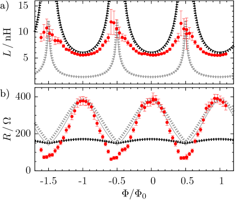
Figure 4 also includes theoretical predictions for two different rates of inelastic scattering. The weaker of the two rates () reproduces well and gives a reasonable prediction for its flux-dependent oscillations. Furthermore, if we could only measure changes in , we might conclude that the predicted flux modulation of is in fair agreement with the experimental data for this moderate value of . However, the absolute value of the prediction for is several times smaller than the observed value at nearly all flux values. This highlights the importance of measuring and without offsets if theories are to be rigorously tested. Note that we can improve the agreement between the predicted and measured , especially around integer values of , by using a very strong inelastic scattering rate of in the theoretical calculation. However, this value of leads to a clear disagreement in the amplitude of the oscillations in as shown in Figure 4b.
Figure 4 also shows the theoretical predictions that include strong spin-flip scattering. By choosing appropriately, the predictions become nearly identical to the case of strong inelastic scattering. Therefore, the conclusions of the previous paragraph also apply to predictions where scattering is spin-flip dominated. Furthermore, the similarity of the predictions shows that, in this parameter regime, the source of additional dephasing is unimportant.
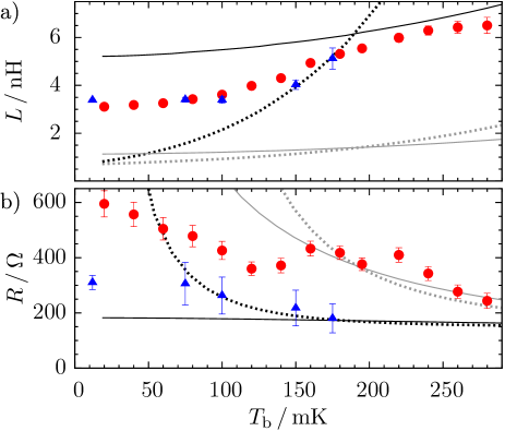
To gain further insight, we study the temperature dependence of and for one resonance from each sample near 1 GHz (see Figure 5). In addition to the measured data points, Figure 5 shows theoretical predictions with scattering parameters that—at 195 mK—are identical to those in Figure 4. However, we note that considerable freedom remains in choosing the temperature dependence of the scattering rates. Rigorously justifying a particular temperature scaling would require knowledge of the specific microscopic mechanism responsible for the scattering. However, as the theoretical predictions already disagree with the measured results at the phenomenological level at a fixed temperature (Figure 4), identifying any specific microscopic mechanism seems implausible. As instructive examples, we choose and a constant in Figure 5. Unsurprisingly, none of the predictions simultaneously matches the observed temperature dependence of and . Nevertheless, the experimental data in Figure 5 may serve an important role in testing alternative theories in the future.
VI Conclusions
The main discrepancy between theory and experiment can be summarized as follows. The proximity effect at and is weaker than what is predicted by theory based on the Usadel equation.Virtanen et al. (2011) This disagreement manifests itself experimentally as measured values that fall below theoretical predictions and measured values that exceed theoretical predictions. As potential candidates for such loss of coherence, we considered inelastic scattering and spin-flip scattering in the weak link. However, we did not find choices of or that would provide simultaneous agreement in and , neither in terms of flux dependence at a fixed bath temperature, nor in terms of temperature-dependence at zero flux bias. Furthermore, the scattering rates required for a match in either or are larger than expected for, e.g., electron–electron scattering in disordered systems.Rammer and Smith (1986)
We note that the discrepancies shown here are not in direct contradiction with the previous experimentsChiodi et al. (2011); Dassonneville et al. (2013) and that both the SNS junctions and the measurement scheme presented here are very different from these preceding studies. Firstly, the weak link material is different than in the previous experiments. We cannot rule out the possibility of effects specific to gold-palladium McGinnis and Chaikin (1985) that reduce coherence in the weak link. Secondly, we measure both the reactive and dissipative components of the electrical admittance without arbitrary offsets. In contrast, only changes in the admittance have been previously reported. Thus, our experimental technique provides a more stringent test of the accuracy of the theory and reveals quantitative disagreements more easily.
In conclusion, we reported measurements of microwave frequency admittance for gold-palladium SNS junctions, together with a comparison to quasiclassical theory for diffusive SNS weak links. These discrepancies between measurement results and theoretical predictions suggest that dephasing caused by inelastic scattering, or elastic spin-flip scattering, is probably not the correct mechanism for explaining why the proximity-induced superconductivity is weaker than expected in our gold-palladium SNS junctions. Further theoretical work is required for reaching simultaneous agreement for the magnitude, temperature dependence, and flux dependence of both the dissipative and reactive parts of the admittance. Mechanisms that may need to be taken into account include imperfect interfaces Heikkilä et al. (2002); Hammer et al. (2007), electron–electron and fluctuation effects in low-dimensional superconducting structures, Narozhny et al. (1999); Semenov et al. (2012) and paramagnon interaction. Kontos et al. (2004) Magnetic effects could be particularly important in SNS junctions that include palladium, which is paramagnetic in bulk and can even become ferromagnetic in nanoscale particles. Shinohara et al. (2003); Sampedro et al. (2003) In general, the relationship between microscopic materials properties and coherence at microwave frequency in normal-metal Josephson junctions should be clarified, both experimentally and theoretically. A productive experimental approach may be to first investigate systems such as Nb/Cu weak links that, based on previous dc experiments,Dubos et al. (2001a); Jabdaraghi et al. (2016) are expected to behave in an ideal fashion at dc.
VII Experimental Section
VII.1 Device fabrication
VII.1.1 Resonators
The substrates are 4” (0.5-mm thick) high-resistivity () Si wafers with 300 nm of thermal oxide. First, a niobium thin film (thickness 200 nm) is sputter deposited on the entire wafer. Next, the coplanar waveguide (CPW) structures are defined with AZ5214E positive photoresist that is reflowed at for 1 min to ensure a positive etch profile of the resulting Nb features. Then CPWs are etched with an rf-generated plasma under a constant flow of SF6(40 sccm)/O2(20 sccm) gases at constant power.Curtis and Mantle (1993) The remaining resist is removed with solvents and an additional O2-plasma cleaning step. The 4” wafer is then coated with a protective layer of resist and pre-diced with partial cuts along device pixel outlines on the back of the wafer.
VII.1.2 Capacitor dielectric
The Al2O3 dielectric for the on-chip Nb-Al2O3-Al capacitors , , and is formed by atomic layer deposition with 455 cycles in a H2O/TMA process at 200 ∘C resulting in a thickness of 42 nm. The thickness was verified in ellipsometry using an index of refraction . Measurements of reference Nb-Al2O3-Al capacitors yield a capacitance per unit area of .
VII.1.3 Nanostructures
The gold-palladium nanowires and aluminum superconducting leads are fabricated by electron beam lithography in two separate evaporation/liftoff steps. In the first step, gold and palladium pellets are evaporated from the same crucible with an electron beam heater. Afterward, unwanted Au-Pd is lifted off with organic solvents. Prior to the evaporation of the Al leads, samples are cleaned in situ with an Ar sputter gun. Finally, after liftoff of the Al film, individual resonator pixels are snapped along the pre-diced lines and packaged for measurement.
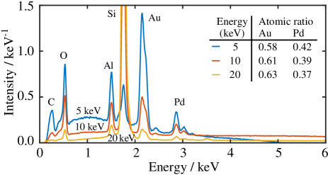
The chemical composition of the gold-palladium material is determined with energy-dispersive X-ray spectroscopy for incident electron beam energies 5 keV, 10 keV, and 20 keV (Figure 6). The average Au:Pd atomic ratio (weight ratio) is approximately 3:2 (3:1)
VII.2 Cryogenic measurements
Measurements are carried out in a commercial cryostat with the base temperature of 10 mK. The transmission coefficient was probed with a vector network analyzer. The device input line had 100 dB fixed attenuation. For all measurements, the output signal is amplified by a broadband low-noise cryogenic amplifier and by additional room temperature amplifiers. For some measurements (e.g. Sample 2, ) two cryogenic isolators are placed on the base cooling stage between the low-noise cryogenic amplifier and the sample. Each sample was placed in a custom printed circuit board and sealed within a metal enclosure. The external flux coil consists of a superconducting solenoid with 100 turns that is fixed outside the metal enclosure. One period in Figure 4 and 5 corresponds to a current change of mA through the coil. Magnetic shielding surrounds both the enclosure and flux-coil in the case of Sample 2.
The measurement power incident at the transmission line input is approximately -128 dBm for the data shown in Figure 4 and 5. This drives a current of roughly 5 nA through the SQUID chain at for of Sample 2. This is far below the estimated critical current of the SQUID chain. Furthermore, experimentally we ensure that we measure the linear response by making sure that the measured is not sensitive to factor-of-two changes in the measurement power.
VII.3 Normalized transmission coefficient
We define the normalized transmission coefficient as , where is the full transmission coefficient, including contributions from the cabling and other external circuitry, and is its best fit to Equation 1. Dividing by removes all flux-independent features introduced external circuitry and unintentional reflections. Multiplying by removes the systematic contribution of the reference, which would otherwise appear at all values of as a static vertically inverted mirror image () of the reference resonance.
The scan used as the reference alternates between and , changing from one to the other whenever crosses , where . This keeps the resonance in the reference far from the resonance frequency at the value being analyzed. These changes in cause the apparent discontinuities in the background color in Figure 2.
Acknowledgements
We thank Leif Grönberg for depositing the Nb used in this work. We acknowledge the provision of facilities and technical support by Aalto University at OtaNano - Micronova Nanofabrication Centre as well as financial support from the Emil Aaltonen Foundation, the European Research Council under Grant 278117 (SINGLEOUT), the Academy of Finland under The COMP Centre of Excellence (251748, 284621) and grants 257088, 265675, 276528, 286215 and the European Metrology Research Programme (EMRP EXL03 MICROPHOTON). The EMRP is jointly funded by the EMRP participating countries within EURAMET and the European Union. We also acknowldege support from Aalto Centre for Quantum Engineering.
References
- Clarke (1968) J. Clarke, Phys. Rev. Lett. 21, 1566 (1968).
- Usadel (1970) K. D. Usadel, Phys. Rev. Lett. 25, 507 (1970).
- Likharev (1979) K. K. Likharev, Rev. Mod. Phys. 51, 101 (1979).
- Dubos et al. (2001a) P. Dubos, H. Courtois, B. Pannetier, F. K. Wilhelm, A. D. Zaikin, and G. Schön, Phys. Rev. B 63, 064502 (2001a).
- Heikkilä et al. (2002) T. T. Heikkilä, J. Särkkä, and F. K. Wilhelm, Phys. Rev. B 66, 184513 (2002).
- Courtois et al. (2008) H. Courtois, M. Meschke, J. T. Peltonen, and J. P. Pekola, Phys. Rev. Lett. 101, 067002 (2008).
- Andreev (1965) A. F. Andreev, Sov. J. Exp. Theor. Phys. 22, 455 (1965).
- Guéron et al. (1996) S. Guéron, H. Pothier, N. O. Birge, D. Esteve, and M. H. Devoret, Phys. Rev. Lett. 77, 3025 (1996).
- le Sueur et al. (2008) H. le Sueur, P. Joyez, H. Pothier, C. Urbina, and D. Esteve, Phys. Rev. Lett. 100, 197002 (2008).
- Notarys et al. (1973) H. A. Notarys, M. L. Yu, and J. E. Mercereau, Phys. Rev. Lett. 30, 743 (1973).
- Warlaumont et al. (1979) J. M. Warlaumont, J. C. Brown, T. Foxe, and R. A. Buhrman, Phys. Rev. Lett. 43, 169 (1979).
- Lehnert et al. (1999) K. W. Lehnert, N. Argaman, H. R. Blank, K. C. Wong, S. J. Allen, E. L. Hu, and H. Kroemer, Phys. Rev. Lett. 82, 1265 (1999).
- Dubos et al. (2001b) P. Dubos, H. Courtois, O. Buisson, and B. Pannetier, Phys. Rev. Lett. 87, 206801 (2001b).
- Fuechsle et al. (2009) M. Fuechsle, J. Bentner, D. A. Ryndyk, M. Reinwald, W. Wegscheider, and C. Strunk, Phys. Rev. Lett. 102, 127001 (2009).
- Chiodi et al. (2009) F. Chiodi, M. Aprili, and B. Reulet, Phys. Rev. Lett. 103, 177002 (2009).
- Virtanen et al. (2010) P. Virtanen, T. T. Heikkilä, F. S. Bergeret, and J. C. Cuevas, Phys. Rev. Lett. 104, 247003 (2010).
- Galaktionov and Zaikin (2010) A. V. Galaktionov and A. D. Zaikin, Phys. Rev. B 82, 184520 (2010).
- Virtanen et al. (2011) P. Virtanen, F. S. Bergeret, J. C. Cuevas, and T. T. Heikkilä, Phys. Rev. B 83, 144514 (2011).
- Kos et al. (2013) F. Kos, S. E. Nigg, and L. I. Glazman, Phys. Rev. B 87, 174521 (2013).
- Ferrier et al. (2013) M. Ferrier, B. Dassonneville, S. Guéron, and H. Bouchiat, Phys. Rev. B 88, 174505 (2013).
- Tikhonov and Feigel’man (2015) K. S. Tikhonov and M. V. Feigel’man, Phys. Rev. B 91, 054519 (2015).
- Chiodi et al. (2011) F. Chiodi, M. Ferrier, K. Tikhonov, P. Virtanen, T. T. Heikkilä, M. Feigelman, S. Guèron, and H. Bouchiat, Sci. Rep. 1, 3 (2011).
- Dassonneville et al. (2013) B. Dassonneville, M. Ferrier, S. Guéron, and H. Bouchiat, Phys. Rev. Lett. 110, 217001 (2013).
- Govenius et al. (2014) J. Govenius, R. E. Lake, K. Y. Tan, V. Pietilä, J. K. Julin, I. J. Maasilta, P. Virtanen, and M. Möttönen, Phys. Rev. B 90, 064505 (2014).
- Govenius et al. (2016) J. Govenius, R. E. Lake, K. Y. Tan, and M. Möttönen, Phys. Rev. Lett. 117, 030802 (2016).
- Pomeroy and Grube (2009) J. M. Pomeroy and H. Grube, J. Appl. Phys. 105, 094503 (2009).
- Wellstood et al. (1994) F. C. Wellstood, C. Urbina, and J. Clarke, Phys. Rev. B 49, 5942 (1994).
- Geerlings et al. (2012) K. Geerlings, S. Shankar, E. Edwards, L. Frunzio, R. J. Schoelkopf, and M. H. Devoret, Appl. Phys. Lett. 100, 192601 (2012).
- Khalil et al. (2012) M. S. Khalil, M. J. A. Stoutimore, F. C. Wellstood, and K. D. Osborn, J. Appl. Phys. 111, 054510 (2012).
- Abrikosov and Gor’kov (1960) A. A. Abrikosov and L. P. Gor’kov, Zh. Eksp. Teor. Fiz. 39, 1781 (1960), [Sov. Phys. JETP, 12, 1243 (1961)].
- Giazotto et al. (2006) F. Giazotto, T. T. Heikkilä, A. Luukanen, A. M. Savin, and J. P. Pekola, Rev. Mod. Phys. 78, 217 (2006).
- Rammer and Smith (1986) J. Rammer and H. Smith, Rev. Mod. Phys. 58, 323 (1986).
- Pierre et al. (2003) F. Pierre, A. B. Gougam, A. Anthore, H. Pothier, D. Esteve, and N. O. Birge, Phys. Rev. B 68, 085413 (2003).
- Huard et al. (2004) B. Huard, A. Anthore, F. Pierre, H. Pothier, N. O. Birge, and D. Esteve, Solid State Commun. 131, 599 (2004).
- Hammer et al. (2007) J. C. Hammer, J. C. Cuevas, F. S. Bergeret, and W. Belzig, Phys. Rev. B 76, 064514 (2007).
- McGinnis and Chaikin (1985) W. C. McGinnis and P. M. Chaikin, Phys. Rev. B 32, 6319 (1985).
- Narozhny et al. (1999) B. N. Narozhny, I. L. Aleiner, and B. L. Altshuler, Phys. Rev. B 60, 7213 (1999).
- Semenov et al. (2012) A. G. Semenov, A. D. Zaikin, and L. S. Kuzmin, Phys. Rev. B 86, 144529 (2012).
- Kontos et al. (2004) T. Kontos, M. Aprili, J. Lesueur, X. Grison, and L. Dumoulin, Phys. Rev. Lett. 93, 137001 (2004).
- Shinohara et al. (2003) T. Shinohara, T. Sato, and T. Taniyama, Phys. Rev. Lett. 91, 197201 (2003).
- Sampedro et al. (2003) B. Sampedro, P. Crespo, A. Hernando, R. Litrán, J. C. S. López, C. L. Cartes, A. Fernandez, J. Ramírez, J. G. Calbet, and M. Vallet, Phys. Rev. Lett. 91, 237203 (2003).
- Jabdaraghi et al. (2016) R. N. Jabdaraghi, J. T. Peltonen, O.-P. Saira, and J. P. Pekola, Appl. Phys. Lett. 108, 042604 (2016).
- Curtis and Mantle (1993) B. J. Curtis and H. Mantle, J. Vac. Sci. Technol. A 11, 2846 (1993).