A Modified and Calibrated Drift-Diffusion-Reaction Model for Time-Domain Analysis of Charging Phenomena in Electron-Beam Irradiated Insulators
Abstract
This paper presents an improved version of the previously proposed self-consistent drift-diffusion-reaction model correcting for non-physical behavior at longer time scales. To this end a novel boundary condition is employed that takes into account the effect of tertiary electrons and a fully dynamic trap-assisted generation-recombination mechanism is implemented. Sensitivity of the model with respect to material parameters is investigated and a calibration procedure is developed that reproduces experimental yield-energy curves for uncharged insulators. Long-time charging and yield variations are analyzed for stationary defocused and focused beams as well as moving beams dynamically scanning composite insulators.
pacs:
77.84.Bw, 79.20.Ap, 79.20.Hx, 72.20.Jv, 02.60.Cb, 02.70.DhI Introduction
Charging phenomena in insulators have long been studied due to their importance in such areas as scanning electron microscopy (SEM), memory-based technologies, particle detectors, ceramic surfaces, industrial cables, and the safety of spacecraft lee2007layer ; vdGraaf2017 ; kulwicki1970diffusion ; bass1998measurements ; vampola1985aerospacer . Probably, the earliest systematic studies of electron-irradiation effects in solids and charging phenomena in insulators, as parts of research on electrets, were carried out by B. Gross who has had a great impact on this research field. In his seminal works on irradiation phenomena gross1957irradiation ; gross1958irradiation Gross investigated the electron trapping and charge buildup in high-resistivity solid insulators bombarded with energetic electrons. Further studies by Gross and coworkers produced new experimental techniques and mathematical models gross1967high ; gross1973charge ; gross1974charge ; gross1974transport .
These and more recent liebl1980sims ; le1989study ; meyza2003secondary ; touzin2006electron ; li2011self ; li2010surface ; walker2016simulations studies have not yet been able to provide a complete and coherent account of all observed phenomena. This could be due to the prevailing emphasis on static (stationary) modelsdionne1975origin ; barut1954mechanism ; henke1979soft rather than time-domain analysis. Studying the dynamics of charging in time domain is especially important in the analysis of response times in particle detectorsvdGraaf2017 and in designing novel scanning strategies for SEMwalker2016simulations . The existing dynamic models are either one-dimensional meyza2003secondary ; touzin2006electron or do not include some of the essential physical processes, e.g., dynamic recombination, trapping, etcli2011self ; li2010surface .
While the prevailing semi-classical Monte-Carlo (MC) method kieft2008refinement makes very few assumptions about the complicated electron-sample interaction process, realizing its full theoretical potential is technically very challenging. First of all, MC simulations are slowed down by the need to continuously update the long-rage electrostatic potential. Secondly, it is computationally difficult to keep track of all the trapped and de-trapped electrons. Finally, achieving acceptable variance not only in particle numbers, but also in the times of events (e.g. emission times), may require a prohibitive number of statistical realizations.
Instead of sampling the probability space, the drift-diffusion-reaction (DDR) approach, mainly used to model low-energy transport in semiconductors entner2007modeling ; markowichsemiconductor , directly describes the space-time evolution of a continuous probability density function. The pertaining partial differential equations are obtained from the semi-classical Boltzmann equation applying the method of moments and a few assumptions about the distribution of particles over the momentum space. From the mathematical point of view the DDR approach assumes that the symmetric part of the secondary electrons (SE) probability density function is isotropic about the origin of the momentum space and is well-described by a shifted Maxwellian distribution.
In our previous publication raftari2015self we argued that the DDR approach can be applied to electron-beam irradiated insulators if the initial high-energy transport stage is approximated by an empirical source function. We showed that this pulsed source function allows modeling both the short-time processes immediately following the primary electron (PE) impact and the long-time charge evolution due to sustained bombardment. Importantly, we demonstrated that the sustained irradiation can also be modeled by a continuous current source, which gives practically the same secondary electron (SE) emission current as the time-averaged SE emission produced by many single-impact pulsed sources.
However, the original DDR model raftari2015self had serious shortcomings as well. First of all, it was not calibrated against experimental data. Although we were able to reproduce any SE yield at a chosen PE energy by tuning a single parameter – the electron emission velocity (surface recombination velocity) at the sample-vacuum interface, it was not clear which yield should be taken as a reference, since yields tend to change over time and depend on beam currents. Secondly, using the same SE emission velocity for all PE energies resulted in curves not fully compatible with published SE yield data over the whole range of PE energies. And more seriously, the model produced nonphysical results in the case of prolonged irradiation. Namely, the surface potential at low PE energies could reach very large positive values, which is not possible, since positive potential attracts secondary electrons back to the sample leading to the neutralization of any potentials exceeding V.
We have identified the main reasons behind the bad long-time behavior of the original DDR approachraftari2015self . These were the employed steady-state generation-recombination model, which is not really suitable for the analysis of transient effects, and the neglected tertiary electron current. Incorporating fully dynamic generation and recombination processes is relatively easy. Here we employ the so-called trap-assisted generation-recombination model, which also reduces the number of equations to be solved and charge species to be tracked.
In hybrid MC-DDR methods li2011self ; li2010surface tertiary currents are estimated with direct MC simulations of particle trajectories. Here we propose an alternative approach that keeps intact the self-consistent nature of the DDR model. Namely, we introduce a novel boundary condition at the sample-vacuum interface that accounts not only for the total number of electrons returning to the sample, but also for the spatial distribution of this tertiary current along the sample interface.
We have also developed and implemented a clear calibration procedure for our DDR model. It uses the fact that certain types of yield measurements – the so-called standard-yield measurements – correspond to the situation where single PE impacts happen sufficiently far enough from each other across the sample surface for their mutual interaction to be neglected. As our code is able to simulate single impacts, its calibration can be performed in this single-impact mode.
In Section II we outline the mathematical details of the modified DDR model. Its physical applicability is further discussed in Section III, where we also investigate the sensitivity of the model, explain our parameter choices, develop a calibration procedure against published experimental data, and compare our results for defocused beams with an alternative one-dimensional approach. Section IV presents further quantitative analysis of more realistic scenarios with focused stationary and moving beams, including a dynamic line-scan of a laterally inhomogeneous target.
II Modified DDR model
In this section we recall the main features of the DDR modelraftari2015self and describe several significant modifications that have been implemented since its introduction.
II.1 Basic equations
The continuum approximation of the equilibrium transport of charged particles in insulators consists of both partial (PDE) and ordinary (ODE) differential equations augmented with a semi-empirical source function accounting for the initial ballistic transport stage. The PDE’s are the Poisson equation for the potential and the transport equations for the free charge density:
| (1) |
| (2) |
| (3) |
with the constitutive relations for the current densities given by
| (4) |
| (5) |
where is the elementary charge, is the electrostatic potential, is the density of free electrons, is the density of trapped electrons, is the density of free holes, is the density of empty traps, the constant is the dielectric constant of vacuum, the function is the (static) relative permittivity of the sample, and are the electron and hole mobilities and and are the diffusion coefficients.
II.2 Generation, recombination, trapping, and de-trapping
In the present modification of the DDR approach the dynamic trap-assisted Shockley-Read-Hall (SRH) generation/recombination model is implemented. Here we explain it along the lines of the PhD study by Robert Entner conducted at TU Wien entner2007modeling . An attractive feature of this model is that there is no need to keep the track of trapped holes as all the relevant physics is already contained in the single equation for the rate of electron trapping:
| (6) |
This process is coupled to the basic equations (1)–(5) and can be divided into four subprocesses illustrated in Fig. 1.
(a) Electron capture: An electron from the conduction band gets trapped at the band-gap of the insulator and the surplus energy of is transmitted to the phonon emission. The average rate of this process is
| (7) |
(b) Hole capture: A trapped electron moves to the valence band and neutralizes a hole (i.e. the hole is captured by the occupied trap), producing a phonon with the energy . The corresponding rate is
| (8) |
(c) Hole emission: An electron leaves a hole in the valence band and is trapped (i.e. the hole is emitted from the empty trap to the valence band). The energy is needed for this process, and the corresponding rate is
| (9) |
(d) Electron emission: A trapped electron moves to the conduction band. The required energy is , and the rate is
| (10) |
In the above equations: and are the electron and hole mean trapping cross sections, is the total density of traps, is the density of trapped electrons, is the thermal velocity, and is the intrinsic carrier density. The spatial variable indicates the possibility of spatial inhomogeneity, i.e., the presence of different adjacent materials.
The initial conditions on and at are set as the corresponding intrinsic carrier densities of the materials under consideration, whereas the initial condition for has been derived based on the assumption of the initial steady state for the density of trapped electrons prior to the start of irradiation (i.e. ) and is set to
| (11) |
II.3 Charge injection
As has been discussed in our earlier work raftari2015self , there are two possibilities within the DDR approach to model charge injection by a low- to moderate-energy electron beam via the source terms and . The first fine-scale model captures the discrete nature of the electron beam. The rate of particle production resolved at the level of pulses produced by individual PE impacts is given by:
| (12) |
where is the logistic function, is the number of the particular individual PE, is the -th PE impact time, and is the generation time of the electron-hole pairs, whose choice is discussed in the next section. With single-impact events, due to a relatively small number of produced pairs, the continuous results of the DDR model should be interpreted as probability densities rather than particle densities, especially at lower PE energies.
The second model is designed for studying the sustained bombardment of the sample and is based on the temporal average of the above pulsed source function:
| (13) |
where is the average electron beam current.
Both source functions contain the semi-empirical distribution function of the charge pairs at the end of the initial generation stage:
| (14) | ||||
where and are the beam energy and the effective landing energy of PE’s, is the surface potential at the point of PE impact, is the pair creation energy, is the maximum PE penetration depth (discussed further in detail), is the center of the Gaussian distribution with the distance of from the sample-vacuum interface, and is the constant corresponding to the backscattering rate. In the hole distribution function the constant is zero, however, it is different from zero in the electron distribution function accounting for the remaining PE’s.
In the continuous irradiation mode we consider two additional modifications of the source functions. One pertains to a defocused beam such that the computational domain is smaller than the beam radius. In this case we use the following distribution function derived from (14) by integrating over horizontal coordinates and enforcing the conservation of the amount of generated charge pairs:
| (15) |
where
| (16) |
| (17) |
and is the radius of the irradiated area (computational domain) at the surface. Accordingly, the beam current can be calculated as
| (18) |
where is the current density. The formula (18) adjusts the beam current to achieve results independent of .
If, on the other hand, the radius of a partially focused beam is smaller than the radius of the computational domain we resort to the following distribution:
| (19) | ||||
Here denotes the beam radius rather than the radius of the computational domain.
II.4 Sample-vacuum interface and tertiary electrons
The boundary conditions on , , at the interfaces of the sample with its holder and at the walls of the vacuum chamber are standard: Dirichlet at ohmic contacts and Neumann to simulate isolation and prevent any currents from flowing through the corresponding interface.
The sample-vacuum interface, however, is not common in DDR-type simulations. Previously raftari2015self we have used a Robin-type boundary condition for at this interface, which sets the SE current density at the level proportional to the charge density at the boundary with the emission velocity controlling the magnitude of the current ( is the outward normal vector at the surface). As mentioned in the Introduction this model does not account for the electrons that are being pulled back to the sample by a positive surface potential – the so-called tertiary electrons (TE’s). This leads to nonphysical results – very strong positive charging of samples under prolonged irradiation with low-energy beams.
Experiments show seiler1983secondary that the energy of secondary electrons, although greater than the electron affinity of the material, rarely exceeds eV. Therefore, even a relatively weak positive potential at the surface will pull back some of the emitted secondary electrons. To account for this tertiary electron current we propose the following modified version of the Robin-type boundary condition at the sample-vacuum interface:
| (20) | ||||
| (21) |
where
| (22) |
| (23) | ||||
| (24) |
| (25) |
and
| (26) |
where is the applied potential at the upper boundary, which in the present study is set to zero (. The term in (20) represents the tertiary electrons current density. The function controls the total magnitude of this current and the factor determines its spatial distribution. We assume that tertiary electrons will re-enter the sample only through regions where the normal component of the electric field is negative. The stronger is the local attractive electric field, the higher is the density of tertiary current at that location.
The function is chosen here in such a way, see (23)–(26), that the magnitude of the total tertiary current varies linearly from zero, when the maximum surface potential is below a certain value , to the value of the total outward SE current, when reaches . This means that the net current through the sample-vacuum interface will be zero if as all SE’s leaving the sample will re-enter the sample as tertiary electrons. Typically this leads to the surface potential never raising above (or ). This choice of is not unique and could be further refined to take the energy spectrum of the SE’s into account. One should also mention that, from the computational point of view, the mesh along the sample-vacuum interface should be fine enough in order to capture the gradient of the potential at the surface.
II.5 Numerical solution
The first step toward obtaining a numerical solution of an equation or a system of equations is to investigate the existence and uniqueness of the solution. With regards to the present model, the consistency analysis relies on previously published results. A detailed investigation concerning the existence and uniqueness of stationary drift-diffusion equations can be found in markowichsemiconductor . In a study conducted by Jerome jerome1985consistency a mathematical analysis of a system solution map for the weak form of the DDR model, which forms a basis for the numerical solution of the model, has been provided. Also, in a follow-up study by Busenberg et al. busenberg1993modeling the wellposedness of a DDR model similar to the present one (with different source/sink terms) has been demonstrated.
The multiscale nature of the problem calls for the same strategy as was used in raftari2015self regarding the scaling of variables. We apply the finite element method (FEM) for the numerical solution of the model equations and implement it as a solver within the COMSOL Multiphysics package. To balance the accuracy and the computational costs a careful strategy is needed. Our investigations show that the best (i.e., most reliable) results are obtained when we use adaptive (or local) mesh refinement, Lagrange shape functions, the fully coupled approach with the Newton-Raphson solver, and an adaptive time-stepping algorithm. The use of the adaptive grid refinement, although costly, alleviates the need for more sophisticated approaches, such as the traditional exponential fitting applied in semiconductor studies polak1987semiconductor ; ten1993exponential . To reduce the computational cost of the adaptive mesh refinement, a simple strategy has been followed by using a combination of both adaptive and local refinement methods. Namely, the adaptive refinement was applied only in the initial simulations to identify the regions where a fine mesh is needed and then the local refinement is used in the follow-up simulations.
In some cases, we reduce the original 3D problem to a 2D problem in the -plane of the cylindrical coordinate system as the geometry, boundary conditions, and the source are all axially symmetric. In the simulations of beam scanning over laterally inhomogeneous samples a fully three-dimensional implementation was used.
III Calibration and comparison
In this section we provide a detailed account of the calibration procedure for alumina and silica, which employs experimental data from the studies by Dawson dawson1966secondary and Young et alyong1998determination , simultaneously explaining the underlying approximations of the DDR approach. We also compare our time-domain simulations with the results of an alternative one-dimensional approach.
III.1 Reproducing the standard yield of insulators
There are two main kinds of yield measurements from insulators: dedicated measurements with homogeneous pure samples dawson1966secondary ; yong1998determination and SEM scans of insulator-containing targets kim2010charging . In the former case often a great care is taken to avoid the charging effects. Typically, a defocused beam, a weak beam current, and a pulse of short duration are used. We define the SE yield free of charging effects as the standard yield and calibrate our code to reproduce such data as close as possible.
Parameters of standard-yield experimentsdawson1966secondary ; yong1998determination (current, pulse duration, irradiation area) imply that the probability for the primary electrons to land anywhere close to each other on the surface is very small. In fact, with defocused beams and low, short-duration currents the expected distance between PE’s is large enough to permit neglecting mutual interaction between any two impact zones. This is the main reason why standard-yield measurement are free of charging effects. The single-impact source function (12) with allows to compute directly the expected number of emitted SE’s per single (isolated) PE impact and is, therefore, applicable for modeling the standard yield. The cross-section of the axially-symmetric configuration used for calibrating the code is shown in Fig. 2. With sufficiently large computational domain the boundary conditions at the sides of the sample have no influence on the SE yield from a single PE impact and were set to Neumann (zero current).
There are two classes of parameters that may be tuned within their physically admissible ranges: those that determine the shape of the source function approximating the initial pair generation and the short-time high-energy transport stage, and the material (bulk) parameters that determine the transport and trapping/de-trapping at much longer time scales. While these time scales may seem well-separated, in the DDR model material parameters, especially the emission velocity , have some influence on the initial transport stage as well.
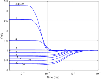
The pair generation time , defined as the time when all pairs have already been generated, determines the time width of the pulsed source functions and of the resulting SE emission current pulse. According to theoretical and experimental investigations by D.I. Vaisburd et al vaisburd2008poole , between and s after impact the generated secondary pairs have already lost their ability to ionize the medium and their energy spectrum begins to evolve away from the spectrum of the primary beam as the result of collisions. However, up to s most of the generated pairs still have energies above 20 eV. Since “true” SE’s dominating the emission spectrum have energies below eV, most of them must be emitted after s. It has also been found that s after impact all generated pairs are already thermalized with their energy spectra tightly localized around the edges of conduction and valence bands and trapping becomes more pronounced. Hence, the SE emission current pulse following a single PE impact should start after s and be almost finished by s. Moreover, if one aims at modeling “true” SE’s, then the relative contribution to the total emission between and s should be small, compared to the contribution between and s. The DDR method produces exactly this type of pulses for set between and s, see Fig. 3. Notably, other parameters influence only the magnitude, not the duration of the emission current pulse.
We emphasize that the curves of Fig. 3 should be interpreted in the probabilistic sense. Namely, the integral of this curve between any two time instants is the number of particles expected to be emitted from the sample surface during the corresponding time interval. Thus, the expected yield at a given PE energy can be computed by numerically integrating the emission current between and some sufficiently large .
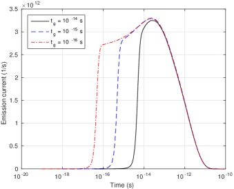
Among the material parameters the carrier mobilities have been determined with the highest precision and are simply assumed here to have the same values as in raftari2015self ; hughes1979generation ; hughes1975hot ; renoud2004secondary . Strictly speaking, these are the so-called low-energy mobilities and a more rigorous approach would be to use femtosecond and picosecond mobilities to model the transport of particles during the corresponding time intervals after the impact vaisburd2008poole . However, mainly due to the absence of data about these high-energy mobilities, here we use the same low-energy mobility values at all times. Nevertheless, the extremely short duration s of the high-energy regime allows us to expect the approximations made in the DDR approach concerning the mobility values during this stage to be appropriate at least in the numerical sense. Notice that the changes in the yield do not exceed when we vary the generation time between and s in Fig. 3. Thus, to have any significant impact on the yield the mobility would have to vary dramatically during this interval of time.
Parameters and related to trapping weakly influence the magnitude of the emission current pulse and have, generally, large uncertainties. For example, in a study set out to investigate electron trapping in alumina pickard1970analysis a relatively large variation of to was reported for the electron capture cross section in polycrystalline alumina. The same study also revealed that polycrystalline metal oxide materials like sapphire (-alumina) generally have trap site densities in the order of . Insulating solids are often grouped into three types: crystals, polycrystalline and amorphouscazaux1996electron . The trap site density has been estimated to be around for an alumina crystal, from to for polycrystals, and around for an amorphous sample.
Probably one of the most comprehensive and systematic studies on charge transport and trapping in silica has been done by DiMaria and co-workers dimaria1979radiation ; dimaria1989trap ; buchanan1989coulombic ; dimaria1991trapping , where a strong link has been identified between the capture cross sections and the nature of traps and the capture cross sections have been estimated to range from to . Confusingly, the values and ranges for these parameters are not limited to the above mentioned estimates ning1976capture ; ning1976high ; williams1965photoemission .
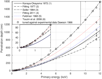
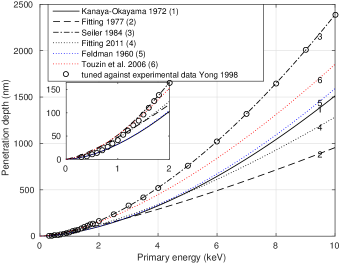
Another parameter that strongly influences the magnitude of the emission current pulse is the maximum PE penetration depth . It determines the spatial shape of the source functions and, therefore, the expected number of particles in the neighborhood of the sample-vacuum interface – the main contributors to the emission current. Many semi-empirical expressions have been proposed for with the following general form , where the values for and vary from study to studyfitting2011secondary ; fitting1977electron . The constant depends on the material and the exponent has been mostly assumed to have a certain material-independent value, although, in some studies has also been considered material-dependentfeldman1960range .
The exponential expression for emanates from Bethe’s theory for the stopping power of charged particles in matter. Bethe’s formula involves the density, atomic number, and atomic weight of the material. However, with the exception of studies by Kanaya and Okayama kanaya1972penetration and by Feldman feldman1960range , the density of the material is considered to be the only parameter influencing the electron penetration depth. As of now the estimation of is far from being certain as can be seen from large discrepancies in the penetration depth estimates employed by different authors, see Fig. 4 (left) and Fig. 5 (left). Apparently, similar disagreement concerning the penetration depth exists for metals as wellcosslett1964multiple .
Having identified , , , and as the most uncertain of the model parameters influencing the magnitude of the emission current pulse we have performed a series of numerical experiments to determine the sensitivity of the DDR model output (SE yield) with respect to changes in these parameters. During these simulations some of the factors would be held fixed while other were varied with the goal to achieve the best possible fit between the computed SE yields and the experimental data. Three key points emerged from this analysis:
-
•
The shape of the yield-energy curve is influenced by the capture cross section and the density of traps. Namely, the larger are the trap density and the capture cross section, the lower is the high-energy tail of the curve.
-
•
The emission velocity affects the height not the shape of the yield-energy curve.
-
•
Following any one of the published penetration depth formulas together with adjusting the values of material parameters within their permitted ranges does not produce yield-energy curves fully compatible with the experimental data over the whole range of PE energies.
In view of these facts and the aforementioned uncertainty about the energy dependence of the penetration depth, fine-tuning for each PE energy against the available experimental data was deemed by us as not only admissible, but also necessary. While tuning other parameters have been fixed at the best found fitting values within their reported ranges. In particular, the electron and hole capture cross-sections were set at the frequently used values of and , respectively. The trap site density turned out to be slightly higher than the reported upper bound , namely, , leading to the initial (equilibrium) density of trapped electrons of , close to what was used by us previouslyraftari2015self .
For PE energies higher than keV the tuned penetration depths for sapphire and silica presented in Fig. 4 (left) and Fig. 5 (left), perfectly match those of Lane and Zaffarano lane1954transmission and are well-described by the formula of Young young1956penetration :
| (27) |
However, according to Young young1956penetration the exponent of is , while the present results agree with the earlier reported lane1954transmission value of . There is some argument about this exponent in the literature. For instance, the study about Kapton and Teflon yang1987electron supports the idea of . Yet, the investigation of Salehi and Flinn salehi1980experimental with materials shows that, although at low energies the exponent is close to , neither nor provide good matches with higher-energy experimental data. The value of was assumed for sapphire in several other investigations as wellmelchinger1995dynamic ; belhaj2000time .
As can be seen from the insets of Fig. 4 (left) and Fig. 5 (left) at energies below keV the tuned penetration depths deviated from the formula (27) and did not follow any other published formulas, while remaining within their range. Least squares fitting of a separate exponential formula of the type (27) to the tuned penetration depths for alumina and silica did not provide a satisfactory fit. This suggests that below keV the energy exponent is indeed material dependent. Hence, for calibration purposes penetration depths bellow keV must be determined by fitting to the corresponding standard yield data, whereas above this energy the depth may be safely deduced from the formula (27).
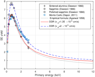
With the tuned penetration depths the DDR method provides practically exact yield-energy curves for the whole range of PE energies. As was mentioned previously, the height of the yield-energy curve is mainly controlled by the electron emission velocity at the vacuum-sample interface. In Fig. 4 (right) we compare the output of the calibrated DDR model with the standard-yield data dawson1966secondary (reported also in the database of Joy Database ), as well as Monte-Carlo simulations dapor2011secondary and the empirical formula of Agarwal agarwal1958variation for alumina samples. As far as the DDR model is concerned the only difference between the unpolished and polished alumina samples is the electron emission velocity at the sample-vacuum interface ( cm/s and cm/s, respectively), which sounds reasonable, since surface polishing should not affect the maximum penetration depth.
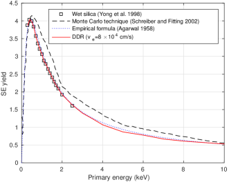
Comparison of the results by the calibrated DDR model with the experimental data yong1998determination , Monte-Carlo simulations schreiber2002monte , and the formula of Agarwal agarwal1958variation for a silica sample is shown in Fig. 5 (right). The tuned electron emission velocity at the silica-vacuum interface ( cm/s) is lower than the emission velocity at the alumina-vacuum interface, indicating that depends on both the material and the surface properties.
DDR simulations indicate that the first and the second unit yields for sapphire occur around eV and keV, respectively. For silica, the unit yields are observed below eV and again at keV. The values of the calibrated material parameters used in the present study are listed in Table 1.
| Parameter | Unit | ||
|---|---|---|---|
| cm2 | |||
| cm2 | |||
| cms-1 | |||
| gcm-3 | |||
| eV | |||
| cm-3 | |||
| cms-1 |
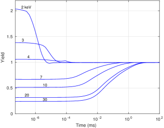
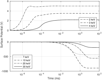
III.2 Continuous irradiation with defocused beams
Sustained bombardment, even with defocused beams, increases the probability for an incoming PE to fall in a close proximity to a previous impact zone. This will introduce the interaction between the previously trapped charges and the newly generated pairs, so that the yield will vary with time.
At the moment a standard experimental procedure for measuring yield variation during sustained bombardment does not exist. Therefore, here we compare predictions of the DDR model with the earlier one-dimensional simulations by the Flight-Drift (FD) model – a self-consistent approach by Touzin et altouzin2006electron . FD model is a current-density based formalism incorporating a detailed recombination and trapping mechanism. For comparison purposes we have considered the same material (amorphous alumina), current density, and the penetration depth formula (energy exponent in (27) is set as ). We switch now to the continuous (time-integrated) source function (13), (15)–(18) suitable for long-time modeling.
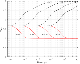
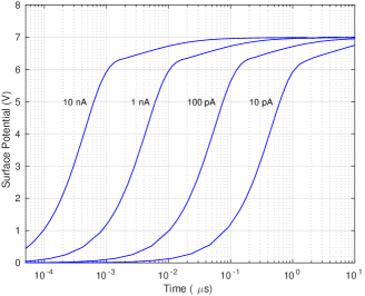
Since the sample is amorphous alumina rather than sapphire, we choose a higher trap density of pertaining to the so-called shallow trapstouzin2006electron . We set the emission velocity to cm/s, close to what we have obtained above for unpolished sapphire. We note that in time-domain investigations the quantity of interest is not the charge yield, but the instantaneous ratio of the net SE emission current to the incident beam current – SE emission rate.
Taking into account that our approach is fundamentally three- not one-dimensional, the results presented in Figs. 6 and 7 show general agreement with the Figures 10 and 11 by Touzin et.al touzin2006electron , especially for the surface potentials at low PE’s and the corresponding SE emission rates. However, at higher PE energies the accumulated negative potential is smaller (lower bounds: kV in 3D-DDR against kV in 1D-FD) and the yield collapses to unity faster (upper bounds: ms in 3D-DDR against ms in 1D-FD).
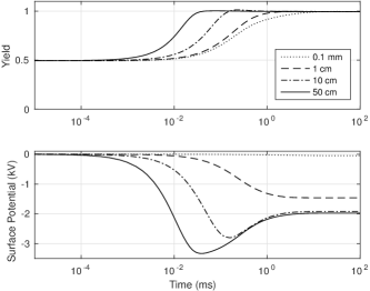
It appears that the distance to the closest Dirichlet boundary, where the electric potential is maintained at some fixed value, e.g., zero, strongly affects the value of the surface potential at the sample-vacuum interface. Apparently, the most important parameter controlling the magnitude of the potential is not the total charge density, as one would naively assume, but the proximity to an ohmic contact. Most likely this is due to the image-charge effect, which partially screens the charge accumulated in the sample.
Things are complicated by the fact that providing at least one Dirichlet boundary condition is essential for the numerical stability (possibly, existence and uniqueness of the solution as well) of the DDR equations. In fact, in the case of an isolated sample, the numerical solution of our nonlinear problem is only possible through the so-called fully coupled approach, since the Dirichlet condition is associated with the Poisson equation, which, therefore, must remain coupled to the rest of equations during the iterations. As the boundary conditions at the interfaces of the sample are not of Dirichlet type, the only available remote surface to impose this type of condition is .
Numerically, the screening effect of the Dirichlet condition can be minimized by placing the ohmic contact as far as computationally possible from the sample surface . Thus, we have placed at various distances from and, as can be seen in Fig. 8, the surface potential does reach significant negative values when the Dirichlet boundary is far enough. However, the time of collapse of yield to unity becomes even shorter in these numerical experiments and remains at odds with the previous one-dimensional FD simulations.
IV Focused and moving beams
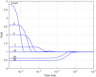
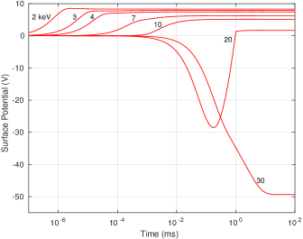
In this section we simulate sustained irradiation of sapphire, silica, and mixed targets by focused stationary and moving electron beams with beam currents typical in SEM. In the first series of numerical experiments we use the axially symmetric target of Fig. 2 illuminated in the middle by a focused stationary beam. The distance between and is set to mm. The samples studied in Fig’s 9–11 are isolated in the sense that the only boundary penetrable for particles in the sample-vacuum interface . We consider the worst case scenario – perfect focusing – where all PE’s hit the same spot on the sample surface. It is easy to deduce that defocusing will affect low-energy PE’s with their small impact zones much stronger than higher energy PE’s with their extended impact zones. To anticipate the results for more realistic partially focused beams the reader is advised to compare plots of this Section IV with those presented in Section III.2.
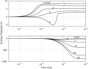
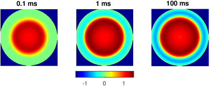
Figure 9 pertains to an unpolished sapphire sample irradiated at keV, where the standard yield is around as can be deduced from Fig. 4 (right). The net SE emission rate – yield for short – starts at the standard yield value, but after a certain interval of time drops to unity for all beam currents. The stronger the current, the shorter is the standard yield interval preceding the drop. In fact, it is easy to calculate that the drop in the yield happens after a certain amount of charge has been injected into the sample by the beam, which confirms conclusions of many previous investigations. The point of fastest decline in the yield roughly corresponds to C of injected primary charge, i.e., approximately primary electrons.
The DDR model does not substantiate the usual intuitive explanationrenoud2004secondary ; touzin2006electron concerning the reasons behind this seemingly inevitable convergence of yield to unity with time. Commonly it is argued that the charging of the sample leads to the change in the landing energy of PE’s, so that the yield no longer corresponds to the standard yield of that energy, but rather to another point on the standard yield curve of Fig. 4 (right). If, for example, the standard yield is greater than one, then the sample accumulates positive charge. The landing energy increases and one should look to the right along the standard-yield curve to know what the new yield should be. If, on the other hand, the standard yield is less than one, then the accumulated negative charge reduces the landing energy of the PE’s, thus, moving to the left along the standard-yield curve. Thus, it is argued, a yield larger than one would eventually lead to a positive potential high enough to shift the landing energy of primary electrons to the second unity-crossing point on the standard yield curve. This argument, while intuitively appealing, does not take into account the spatial distribution, the dynamics, and the screening of charges. In fact, in our simulations the accumulated potential was never strong enough for the landing energy to reach a unity-crossing point.
For example, Figure 9 (bottom) clearly shows that the value of the positive surface potential is insignificant with respect to the PE energy and cannot possibly change the landing energy by so much that it becomes keV – the second point along the standard-yield curve where it crosses the unity line. What the DDR model shows, though, is that the drop in the yield coincides with the rapid increase in the tertiary current, caused by the relatively weak positive surface potential attracting low-energy SE’s back to the sample. Figure 9 (top) compares the contribution of the positive part of the emission current density (dashed lines) to the net SE emission rate (solid lines). The onset of the tertiary current can be deduced from the emergent discrepancy between the solid and dashed curves, which coincides with the positive surface potential reaching the value V in the bottom plot of Fig. 9. Moreover, tertiary current remains significant even after the net yield reaches unity. Thus, the unity yield is the product of a neat dynamic balance between the PE injection, positive outward SE emission, and the reverse tertiary current. The result is a steady-state process and the conservation of total charge (on average): one PE in, one SE out, and a conserved ‘circular’ current at the sample-vacuum interface.
Figure 10 (sapphire) and Figure 11 (silica) correspond to the beam current of pA and show the time evolution of the yield and potential for various PE energies. Comparison with the defocused beam irradiation of Fig’s. 6–7 reveals a larger discrepancy in convergence times of the yield to unity for different energies in the focused beam case. The yield drops much sooner at lower PE energies than it increases at higher PE energies.
Similarly, from the surface potential plots of Fig’s 10–11 we conclude that the rise of sub-unit yields (above keV for sapphire and above keV for silica) to unity cannot be explained by the change in the landing energy, as the associated potential is never negative enough for that. Minimizing the screening by removing the Dirichlet boundary farther away from the sample-vacuum interface we could bring the surface potential in silica down to kV, which, however, was still not enough to decrease the landing energy of PE’s from keV down to the required keV, where the standard yield of silica is equal to one. We propose a much simpler alternative explanation: sub-unit yields increase the number of free electrons near the sample-vacuum interface, which, in its turn, increases the SE emission rate up until the steady-state condition of unit yield is reached. Sometimes, as at keV in sapphire and at keV in amorphous alumina, the yield grows so fast that there is an overshoot, and it temporarily becomes larger than one, causing a positive surface potential, which creates the tertiary current pulling the yield back to unity.
The yield does not always have to drop/increase to unity, though. If it was the case, all insulators would look exactly the same under SEM. One possible scenario, where the yield may not converge to unity, is a (partially) grounded sample. The condition on charge conservation that requires a unit yield in an isolated sample may be relaxed if the sample is grounded. It is, of course, an open question whether a contact between an insulator and, say, a metallic grounded holder can ever be made efficient enough to allow for an easy passage of charges. Assuming for simplicity a perfect ohmic contact, the charge conservation no longer requires the exact unit yield for the sample-vacuum interface as additional electrons may enter the sample via the ground channel. This situation is illustrated in Fig. 12, where we have imposed an ohmic boundary condition on the side of sapphire sample. Although the yield in such a grounded sample does not stay at the level of the standard yield at that energy, after a few oscillations it stabilizes at a slightly lower value, well above unity. This effect is also observed in samples with a relatively poor ground contact described by a Robin-type boundary condition with a low surface recombination velocity.
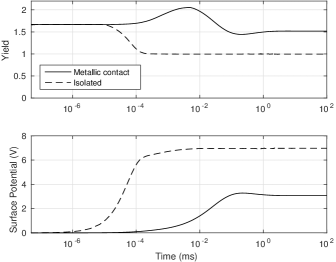
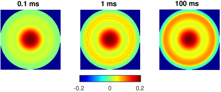
Although, the surface potential does take longer to build up in a sample with contact, Fig. 12 (bottom), the behavior of the surface potential at the injection point is not very revealing. It is, perhaps, more instructive to look at the distribution of the total charge at the surfaces of isolated and grounded samples under identical irradiation conditions. While the surface potential is weaker in the grounded case, Fig. 12 (bottom), the images of Fig. 13 explicitly show that the amount of accumulated positive charge at the surface of a grounded sample is higher. Also the spatial distributions of the surface charge are different. A large disk of positive charge surrounded by a ring of negative charge is seen in the grounded sample, whereas, in the isolated sample most of the positive surface charge is concentrated around the injection point followed by a weaker positive ring some distance away.
Another situation well-known to SEM practitioners where the yield does not drop/increase to unity is the rapid scanning of the sample by a moving focused beam. To simulate the scanning process the source function (14) has to be modified to account for the motion of the beam. This is achieved by setting , where is the velocity of beam displacement in the horizontal plane. Consider a sample surface imaged with a pixels resolution at the rate of frames per second. Then, the beam moves across the sample with the horizontal speed m/s.
We consider an inhomogeneous sample consisting of adjacent blocks of sapphire and silica, see Fig. 14. Samples consisting of one insulator on top of another have been previously studied with a one-dimensional approach cornet2008electron , while vertical stacks of insulators, similar to the one considered here, have been recently investigated experimentally kim2010charging .
We simulate a single scan line through the middle of the sample perpendicular to the interface between the adjacent insulators. Across the vertical interface between the two different insulators the source function (14) exhibits a discontinuity due to the change in material density and the corresponding maximum PE penetration depth.
Since cylindrical symmetry is lost, the following DDR computations had been performed in the full three-dimensional mode. Figure 15 shows the yield as a function of the beam position along its trajectory for an isolated sample. These curves correspond to the intensity of pixels in a single-line SEM image. The standard yields of both insulators at the considered PE energy are also shown as dotted lines.
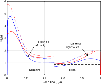
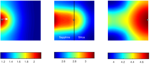
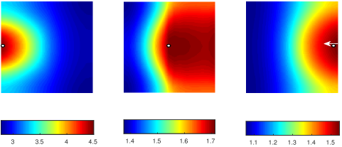
First of all we notice the difference between the left-to-right (from sapphire to silica) and the right-to-left (from silica to sapphire) scanning modes. This difference is easy to understand by looking at Fig. 16 where the images show the surface potential at the same beam locations during these two scans. Since the charging of sapphire is stronger than that of silica, the resulting residual charge strongly depends on the scan history.
Otherwise, the scans of Fig. 15 have several common features. One can notice higher yields in the neighborhood of the sample edges due to increased emission via the vertical interfaces. This is a well-known effect – the sample edges look brighter in SEM images compared to the rest of the sample surface. One can also see the drop of the yield to unity during left-to-right scanning due to continuous charging of the sapphire part. This charging also causes the yield in silica part to drop below its standard value. The relatively smaller charging during the right-to-left scanning does not allow the yield in silica to reach its standard below-unity value after the initial edge-related surge, and keeps the yield below the standard value when the beam crosses into the sapphire part. Additional simulations show that reducing the beam current (down to a few pA) while maintaining a high beam displacement velocity gives scans that truthfully reflect the standard yields of each part of the sample. Unfortunately, in practice this would, probably, result in a bad signal to noise ratio.
V Conclusions
The self-consistent DDR method proposed in raftari2015self has been substantially modified in the present paper to include the dynamic trap-assisted generation-recombination model and a novel self-consistent boundary condition accounting for tertiary electrons. The method has been calibrated against experimental data do deliver exact standard yields for alumina and silica samples over a large range of PE energies. For alumina and silica all calibrated parameters remain within or close to their reported uncertainty bounds, thereby further confirming the acceptability of model approximations. Time-domain simulations with defocused beams have been compared to the previously published results from a one-dimensional Flight-Drift model demonstrating similar long-time behavior. Our investigations so far show that the initial high-energy transport stage can, indeed, be approximated by a semi-empirical source function and low-energy material parameters, whereas, subsequent transport stages fall within the original domain of validity of the low-energy DDR method.
Simulations with stationary focused beams confirm that in electrically isolated samples the yield collapses to unity after a certain number of primary electrons, which depends on the PE energy, has been injected roughly at the same location on the sample surface. However, our simulations do not support the widespread intuitive explanation of this phenomenon in terms of the changing landing energy of PE’s. The effect appears to have dynamic origins and is related to tertiary currents and transient changes in the distribution of charges close to the sample surface.
The surface potential is strongly affected by the proximity of metallic grounded surfaces due to the associated charge screening. This may lead to misinterpretation of charging effects, if one relies solely on the surface potential measurements, but also may present an opportunity to alleviate SEM image distortions. Our simulations show that a good ground contact could also prevent the collapse of the yield to unity.
We have presented, probably, the first 3D simulations of a laterally inhomogeneous sample irradiated by a moving beam that take into account both the dynamic charge trapping/de-trapping and the tertiary electrons. While to a certain extent the yield obtained during this realistic simulations could be interpreted on the basis of time-domain results with stationary beams, some effects are unique to dynamic scanning. For example, the scan profile appears to depend on the direction of scanning.
A recent review by Walker et al walker2016simulations mentions the lack of reliable simulations related to low-energy SEM studies. We hope to partly fill this gap with the present modified and calibrated version of the DDR method. Our method as well as other simulation software would greatly benefit from publicly available high-quality time-domain data in addition to the already available standard yields. While we realize that direct time-domain sampling of detector currents may be difficult, it should be possible to collect and publish single line scans of insulator targets for a rage of dwell times (scan speeds).
Acknowledgements
The authors acknowledge the partial financial support of the Thermo Fisher Scientific (formerly FEI, Netherlands) and many fruitful discussions with H. van der Graaf, C.W. Hagen, S. Tao, A.M.M.G. Theulings, and H.-W. Chan (all from Charged Particle Optics group at Delft University of Technology).
References
- (1) AD Bass, P Cloutier and L Sanche. Measurements of charge accumulation induced by monochromatic low-energy electrons at the surface of insulating samples. Journal of applied physics, 84(5), 2740–2748, 1998.
- (2) H. van der Graaf, H. Akhtar, N. Budko, H.W. Chan, C.W. Hagen, C.C.T. Hansson, G. Nützel, S.D. Pinto, V. Prodanović, B. Raftari, P.M. Sarro, J. Sinsheimer, J. Smedley, S. Tao, A.M.M.G. Theulings, C. Vuik. The Tynode: a new vacuum electron multiplier. Nuclear Instruments and Methods in Physics Research A 847, 148–161, 2017.
- (3) JS Lee and J Cho and C Lee and I Kim and J Park and YM Kim and H Shin and J Lee and F Caruso. Layer-by-layer assembled charge-trap memory devices with adjustable electronic properties. Nature nanotechnology, 2(12), 790–795, 2007.
- (4) BM Kulwicki and AJ Purdes. Diffusion potentials in BaTiO3 and the theory of PTC materials. Ferroelectrics, 1(1), 253–263, 1970.
- (5) Vampola, AL and Mizera, PF and Koons, HC and Fennell, JF and Hall, DF. The Aerospace Spacecraft Charging Document. No. SD-TR-0084A (5940-05)-10. AEROSPACE CORP EL SEGUNDO CA LAB OPERATIONS, 1985.
- (6) B Gross. Irradiation effects in borosilicate glass. Physical Review, 107(2), 368–374, 1957.
- (7) B Gross. Irradiation effects in Plexiglas. Journal of Polymer Science, 27(115), 135–143, 1958.
- (8) B Gross and S.V Nablo. High Potentials in Electron-Irradiated Dielectrics. Journal of Applied Physics, 38(5), 2272–2275, 1967.
- (9) B Gross, J Dow and S.V Nablo. Charge buildup in electron-irradiated dielectrics. Journal of Applied Physics, 44(6), 2459–2463, 1973.
- (10) B Gross,GM Sessler and JE West. Charge dynamics for electron-irradiated polymer-foil electrets. Journal of Applied Physics, 45(7), 2841–2851, 1974.
- (11) B Gross and LN de Oliveira. Transport of excess charge in electron-irradiated dielectrics. Journal of Applied Physics, 45(11), 4724–4729, 1974.
- (12) R Le Bihan. Study of ferroelectric and ferroelastic domain structures by scanning electron microscopy. Ferroelectrics, 97(1), 19–46, 1989.
- (13) H Liebl. SIMS instrumentation and imaging techniques. Scanning, 3(2), 79–89, 1980.
- (14) X Meyza, D Goeuriot, C Guerret-Piécourt, D Tréheux and H-J Fitting. Secondary electron emission and self-consistent charge transport and storage in bulk insulators: Application to alumina. Journal of applied physics, 94(8), 5384–5392, 2003.
- (15) M Touzin, D Goeuriot, C Guerret-Piécourt, D Juvé, D Tréheux and H-J Fitting. Electron beam charging of insulators: A self-consistent flight-drift model. Journal of applied physics, 99(11), 114110, 2006.
- (16) GHC Walker, L Frank and I Müllerová. Simulations and measurements in scanning electron microscopes at low electron energy. Scanning, 9999, 1–17, 2016.
- (17) Wei-Qin Li, Kun Mu and Rong-Hou Xia. Self-consistent charging in dielectric films under defocused electron beam irradiation. Micron, 42(5), 443–448, 2011.
- (18) Wei-Qin Li and Hai-Bo Zhang. The surface potential of insulating thin films negatively charged by a low-energy focused electron beam. Micron, 41(5), 416–422, 2010.
- (19) GF Dionne. Origin of secondary-electron-emission yield-curve parameters. Journal of Applied Physics,46(8), 3347–3351, 1975.
- (20) LB Henke, J Liesegang and SD Smith. Soft-x-ray-induced secondary-electron emission from semiconductors and insulators: Models and measurements. Physical review B,19(6), 3004, 1979.
- (21) AO Barut. The mechanism of secondary electron emission. Physical Review,93(5), 981, 1954.
- (22) E Kieft and E Bosch. Refinement of Monte Carlo simulations of electron–specimen interaction in low-voltage SE. Journal of Physics D: Applied Physics, 41(21), 215310, 2008.
- (23) R Entner. Modeling and simulation of negative bias temperature instability. 2007.
- (24) PA Markowich, C Ringhofer, and C Schmeiser. Semiconductor equations. Springer-Verlag New York, Inc., 1990.
- (25) Raftari B and Budko NV and Vuik C. Self-consistent drift-diffusion-reaction model for the electron beam interaction with dielectric samples. Journal of Applied Physics, 118(20):204101, 2015.
- (26) Jerome, Joseph W. Consistency of semiconductor modeling: an existence/stability analysis for the stationary van Roosbroeck system. SIAM journal on applied mathematics, 45(4): 565–590, 1985.
- (27) Jerome, Joseph W. Modeling and analysis of laser-beam-induced current images in semiconductors. SIAM journal on applied mathematics, 53(1): 187–204, 1993.
- (28) SJ Polak, C Den Heijer, WHA Schilders and P Markowich. Semiconductor device modelling from the numerical point of view. International Journal for Numerical Methods in Engineering, 24(4): 763–838, 1987.
- (29) JHM Ten Thije Boonkkamp and WHA Schilders. An exponential fitting scheme for the electrothermal device equations specifically for the simulation of avalanche generation. COMPEL-The international journal for computation and mathematics in electrical and electronic engineering, 12(2): 95–111, 1993.
- (30) PH Dawson. Secondary electron emission yields of some ceramics. Journal of Applied Physics, 37(9), 3644–3645, 1966.
- (31) S Michizono, Y Saito, S Yamaguchi, S Anami, N Matuda and A Kinbara, A. Dielectric materials for use as output window in high-power klystrons. IEEE transactions on electrical insulation, 28(4), 692–699, 1993.
- (32) J Barnard, I Bojko, and N Hilleret. Measurements of the secondary electron emission of some insulators. Internal Note (CERN), 1997.
- (33) PH Dawson. Determination of secondary electron yield from insulators due to a low-kV electron beam. Journal of applied physics, 84(8), 4543–4548, 1998.
- (34) Kim, Ki Hyun and Akase, Zentaro and Suzuki, Toshiaki and Shindo, Daisuke. Charging effects on SEM/SIM contrast of metal/insulator system in various metallic coating conditions. Materials transactions, 51(6), 1080–1083, 2010.
- (35) Paul S Pickard and Monte V Davis. Analysis of electron trapping in alumina using thermally stimulated electrical currents. Journal of Applied Physics, 41(6), 2636–2643, 1970.
- (36) J Cazaux. Electron Probe Microanalysis of Insulating Materials: Quantification Problems and Some Possible Solutions. X-Ray Spectrometry, 25(6), 265–280, 1996.
- (37) DJ DiMaria, LM Ephrath, and DR Young. Radiation damage in silicon dioxide films exposed to reactive ion etching. Journal of Applied Physics, 50(6), 4015–4021, 1979.
- (38) DJ Dimaria and JW Stasiak. Trap creation in silicon dioxide produced by hot electrons. Journal of Applied Physics, 65(6), 2342–2356, 1989.
- (39) DA Buchanan, MV Fischetti, and DJ DiMaria. Coulombic and neutral trapping centers in silicon dioxide. Physical Review B, 43(2), 1471, 1991.
- (40) DA Buchanan and and JH Stathis. Trapping and trap creation studies on nitrided and reoxidized-nitrided silicon dioxide films on silicon. Journal of applied physics, 70(3), 1500–1509, 1991.
- (41) H-J Fitting, H Glaefeke, and W Wild. Electron penetration and energy transfer in solid targets. physica status solidi (a), 43(1), 185–190, 1977.
- (42) H-J Fitting and M Touzin. Secondary electron emission and self-consistent charge transport in semi-insulating samples. Journal of Applied Physics, 110(4):044111, 2011.
- (43) Ch Feldman. Range of 1-10 keV electrons in solids. Physical Review, 117(2), 455, 1960.
- (44) Ch Feldman. Penetration and energy-loss theory of electrons in solid targets. Journal of Physics D: Applied Physics, 5(1) 43, 1972.
- (45) RO Lane and DJ Zaffarano. Transmission of 0-40 keV electrons by thin films with application to beta-ray spectroscopy. Physical Review, 94(4) 960, 1954.
- (46) JR Young. Penetration of electrons in aluminum oxide films. Physical Review, 103(2) 292, 1956.
- (47) KY Yang and RW Hoffman. Electron yields and escape depths from Kapton and Teflon. Surface and Interface Analysis, 10(2-3) 121–125, 1987.
- (48) M Salehi and EA Flinn. An experimental assessment of proposed universal yield curves for secondary electron emission. Journal of Physics D: Applied Physics, 13(2) 281, 1980.
- (49) Melchinger, A and Hofmann, S. Dynamic double layer model: Description of time dependent charging phenomena in insulators under electron beam irradiation. Journal of applied physics, 78(10) 6224–6232, 1995.
- (50) M Belhaj, S Odof, K Msellak and O Jbara. Time-dependent measurement of the trapped charge in electron irradiated insulators: application to Al2O3–sapphire. Journal of applied physics, 88(5) 2289–2294, 2000.
- (51) DC Joy. A database of electron-solid interactions, revision 08-1, 2008.
- (52) M Dapor. Secondary electron emission yield calculation performed using two different Monte Carlo strategies. Nuclear Instruments and Methods in Physics Research Section B: Beam Interactions with Materials and Atoms, 269(14), 1668–1671, 2011.
- (53) BK Agarwal. Variation of secondary emission with primary electron energy. Proceedings of the Physical Society, 71(5), 851, 1958.
- (54) E Schreiber and HJ Fitting. Monte Carlo simulation of secondary electron emission from the insulator SiO2. Journal of Electron Spectroscopy and Related Phenomena, 124(1), 25–37, 2002.
- (55) VE Cosslett and RN Thomas. Multiple scattering of 5-30 keV electrons in evaporated metal films II: Range-energy relations. British Journal of Applied Physics, 15(11), 1283, 1964.
- (56) S Fakhfakh, O Jbara, S Rondot, A Hadjadj and Z Fakhfakh. Experimental characterisation of charge distribution and transport in electron irradiated PMMA. Journal of Non-Crystalline Solids, 358(8), 1157–1164, 2012.
- (57) K Said, G Damamme, A Si Ahmed, G Moya, A Kallel. Dependence of secondary electron emission on surface charging in sapphire and polycrystalline alumina: Evaluation of the effective cross sections for recombination and trapping. Applied Surface Science, 297, 45–51, 2014.
- (58) R Renoud, F Mady, C Attard, J Bigarre, J-P Ganachaud. Secondary electron emission of an insulating target induced by a well-focused electron beam–Monte Carlo simulation study. physica status solidi (a), 201(9), 2119–2133, 2004.
- (59) N. Cornet, D. Gœuriot, C. Guerret-Piecourt, D. Juvé, D. Tréheux, M. Touzin, H-J. Fitting. Electron beam charging of insulators with surface layer and leakage currents. Journal of Applied Physics, 103(6), 064110, 2008.
- (60) H Seiler. Secondary electron emission in the scanning electron microscope. Journal of Applied Physics, 54(11), R1–R18, 1983.
- (61) RC Hughes. Generation, transport, and trapping of excess charge carriers in Czochralski-grown sapphire. Physical Review B, 19(10), 5318, 1979.
- (62) RC Hughes. Hot Electrons in SiO2. Physical Review Letters, 35(7), 449, 1975.
- (63) D.I. Vaisburd,K.E. Evdokimov. The Poole–Frenkel effect in a dielectric under nanosecond irradiation by an electron beam with moderate or high current density. Russian Physics Journal, 51(12), 1255–1261, 2008.
- (64) TH Ning. Capture cross section and trap concentration of holes in silicon dioxide. Journal of Applied Physics, 47(3), 1079–1081, 1976.
- (65) TH Ning. High-field capture of electrons by Coulomb-attractive centers in silicon dioxide. Journal of Applied Physics, 47(7), 32–3208, 1976.
- (66) R Williams. Photoemission of electrons from silicon into silicon dioxide. Physical Review, 140(2A), A569, 1965.