Exciton formation assisted by longitudinal optical phonons in monolayer transition metal dichalcogenides
Abstract
We examine a mechanism by which excitons are generated via the LO (longitudinal optical) phonon-assisted scattering process after optical excitation of monolayer transition metal dichalcogenides. The exciton formation time is computed as a function of the exciton center-of-mass wavevector, electron and hole temperatures, and carrier densities for known values of the Fröhlich coupling constant, LO phonon energy, lattice temperature, and the exciton binding energy in layered structures. For the monolayer MoS2, we obtain ultrafast exciton formation times on the sub-picosecond time scale at charge densities of 5 1011 cm-2 and carrier temperatures less than 300 K, in good agreement with recent experimental findings ( 0.3 ps). While excitons are dominantly created at zero center-of-mass wavevectors at low charge carrier temperatures ( 30 K), the exciton formation time is most rapid at non-zero wavevectors at higher temperatures ( 120 K) of charge carriers. The results show the inverse square-law dependence of the exciton formation times on the carrier density, consistent with a square-law dependence of photoluminescence on the excitation density. Our results show that excitons are formed more rapidly in exemplary monolayer selenide-based dichalcogenides (MoSe2 and WSe2) than sulphide-based dichalcogenides (MoS2 and WS2).
I Introduction
Exciton mediated many-body interactions give rise to a host of physical effects Qiu et al. (2016); Sahin et al. (2016); Cudazzo et al. (2016) that determine the opto-electronic properties of low dimensional transition metal dichalcogenides, MX2 (M = Mo, W, Nb and X = S, Se) Scharf et al. (2016); Ramasubramaniam (2012); Ugeda et al. (2014); Wang et al. (2012); Mak et al. (2010); Qiu et al. (2013); Splendiani et al. (2010a); Komsa and Krasheninnikov (2012); Kormányos et al. (2013), with important consequences for fundamental and applied research. The confinement of correlated charge carriers or excitons to a narrow region of space in low dimensional transition metal dichalcogenides (TMDCs) leads to unique photoluminescence properties Pospischil et al. (2016b); Plechinger et al. (2012); Gao et al. (2016); Ji et al. (2013); Zhu et al. (2016); Eda and Maier (2013); Ghatak et al. (2011); Berghäuser and Malic (2013); Molina-Sánchez et al. (2013); Mai et al. (2013) that are otherwise absent in the bulk configurations Saigal et al. (2016). The availability of state-of-the art exfoliation techniques Novoselov et al. (2005); Varrla et al. (2015); Chen et al. (2015); Fan et al. (2015) enable fabrication of low dimensional transition metal dichalcogenides that is useful for applications Ou et al. (2014); Li et al. (2016); Perebeinos (2015); Beck et al. (2000); Tsai et al. (2013); Bernardi et al. (2013); He et al. (2012); Wi et al. (2014); Bertolazzi et al. (2013); Ji et al. (2013); Yu et al. (2016); Park et al. (2016); Eda and Maier (2013); Radisavljevic et al. (2011); Lembke et al. (2015); Pospischil et al. (2014); Zhang et al. (2014); Yoon et al. (2011). The excitonic processes that determine the performance of TMDC-based electronic devices include defect assisted scattering and trapping by surface states Shi et al. (2013), decay via exciton-exciton annihilation Shin et al. (2014); Ye et al. (2014); Konabe and Okada (2014), phonon assisted relaxation Thilagam (2016), and capture by mid-gap defects through Auger processes Wang et al. (2015). Excitonic processes that result in the formation of complex trions Mak et al. (2013); Berkelbach et al. (2013); Thilagam (1997) and electron-hole recombination with generation of hot carriers Kozawa et al. (2014) are also of importance in device performances.
Dynamical processes incorporating exciton-phonon interactions underlie the opto-electronic properties of monolayer transition metal dichalcogenides Jones et al. (2013). The strength of the interactions between coupled charge carriers and phonons is deduced from experimental measurements of the dephasing times Nie et al. (2014), exciton linewidths Selig et al. (2016), photoluminescence, Mouri et al. (2013a) and other parameters such as the exciton mobility and luminescence rise times. The exciton formation time is determined by a complicated interplay of various dynamical processes in the picosecond time scale Siantidis et al. (2001) and is linked to the efficient operation of optoelectronic devices. To this end, a comprehensive understanding of how newly generated electron-hole pairs relax energetically to form excitons still remain unclear. Recently decay times of 0.3 ps of the transient absorption signal subsequent to the interband excitation of the monolayer WSe2, MoS2, and MoSe2 was recorded in time-resolved measurements Ceballos et al. (2016). The ultrafast decay times were deduced as the exciton formation times from electron-hole pairs in monolayer systems. Motivated by these considerations, we examine a mechanism by which excitons are formed from an initial state of unbound electron-hole pairs to account for the observed short exciton formation time Ceballos et al. (2016) in common TMDCs (MoS2, MoSe2, WS2, and WSe2). While the focus of this paper is on the theoretical aspects of excitonic interactions, the overall aim is to seek an understanding of the critical factors that limit the exciton formation time which is of relevance to experimental investigations involving device applications.
The unequal charges of the basis atoms in polar crystals allow a moving electron to polarize the electric field of its surrounding medium. The polarization effects displaces the ions giving rise to lattice vibrations of a optical phonon frequency in resonance with the polarization field, and enable direct Fröhlich coupling between phonons and charge carriers. In this work we consider that the excitons are created via the two-dimensional Fröhlich interaction which provides a critical pathway by which charge carriers undergo energy loss to optical phonons at elevated temperatures in the monolayers MoS2 and other transition-metal dichalcogenides Kaasbjerg et al. (2014). The exciton is a neutral quasiparticle, and polarization effects due to the longitudinal optical waves may appear to have less influence than those associated with polarization effects of the individual electron or hole. In reality the internal state of the exciton undergoes dipole type transitions and there occurs measurable effects due to Fröhlich interactions in constrained systems. The focus on LO phonons in the exciton formation process in this study is justified by the large strength of excitonic interactions with high frequency phonons that arise due to the strong confinement of the exciton wave-functions in the real space of monolayer systems. Moreover the exciton-phonon interaction is long ranged due to the existence of polarization effects despite large separations between charge carriers and the ions in the material system. The phonon-limited mobility is largely dominated by polar optical scattering via the Fröhlich interaction at room temperatures Kaasbjerg et al. (2012). Exciton formation may take place via deformation potential coupling to acoustic phonons Oh and Singh (2000); Thilagam and Singh (1993), but is likely to occur with less efficiency due to the high exciton binding energies Mak et al. (2010); Cheiwchanchamnangij and Lambrecht (2012); Ugeda et al. (2014); Hill et al. (2015); Cheiwchanchamnangij and Lambrecht (2012); Komsa and Krasheninnikov (2012); Thilagam (2014a) in monolayer dichalcogenides.
In conventional semiconductors such as the two band GaAs material system, excitons are formed via the Fröhlich interaction in the picosecond time range Siantidis et al. (2001); Oh et al. (2000). While excitons in GaAs materials are dominantly formed at the center of the Brillouin zone center, the formation process occurs at the non-central points in the momentum space of monolayer TMDCs Jones et al. (2013). This gives rise to quantitative differences in the exciton creation times between GaAs and TMDCs. For excitation energies higher than the band-gap of monolayer systems, the electron-hole pair creates an exciton with a non-zero wavevector associated with its center-of-mass motion Siantidis et al. (2001); Oh et al. (2000). The exciton subsequently relaxes to the zero wavevector state with emission of acoustic or LO phonons before undergoing radiative recombination by emitting a photon. To this end, the formation time of an exciton as a function of exciton wave vector is useful in analyzing the luminescence rise times that can be measured experimentally.
In this study we employ the exciton-LO phonon interaction operator to estimate the exciton formation times in monolayer transition metal dichalcogenides. The formation time of excitons is determined using the interaction Hamiltonian which describes the conversion of the photoexcited free electron-hole pair to a final exciton state initiated by exciton-phonon Fröhlich interactions, and accompanied by absorption or emission of phonons. The dependence of the exciton formation time on several parameters such as the temperatures of the crystal lattice, charge carriers and excitons as well as the densities of charge carriers and excitons will be closely examined in this study.
II Formation of Excitons in monolayer Molybdenum Disulfide
II.1 Exciton-LO phonon Hamiltonian
We project the single monolayer of a hexagonally ordered plane of metal atoms sandwiched between two other hexagon planes of chalcogens onto a quasi two-dimensional space Cho et al. (2008); Mouri et al. (2013b). The motion of the exciton is generally confined to the parallel two-dimensional layers of the atomic planes with restricted electron and hole motion in the direction perpendicular to the monolayer plane. The monolayer MoS2 has nine phonon branches consisting of three acoustic and six optical branches. The two lowest optical branches are weakly coupled to the charge carriers are therefore not expected to play a significant role in the creation of excitons. The next two phonon branches at the point positioned at energies 48 meV Kaasbjerg et al. (2012) are linked to polar optical modes, which play a critical role in the formation of exciton after photoexcitation of the material system. The roles of the homopolar dispersionless mode at 50 meV which typically occurs in layered structures as well as the sixth phonon mode with the highest energy will not be considered here. Due to the large difference in momentum between valleys in TMDCs, we assume that the exciton formation occurs via an LO phonon-assisted intravalley process which preserves the valley polarization in the monolayer system.
The Hamiltonian term associated with the interaction between excitons and LO phonons is obtained by summing the electron-LO phonon and hole-LO phonon interaction Hamiltonians as follows
| (1) | |||||
| (2) |
where and denote the respective space coordinates of the electron and hole, and (or ) marked with an arrow denotes the monolayer in-plane coordinates of the electron (or hole). The phonon creation and annihilation operators are denoted by and , respectively, where is composed of the in-plane and perpendicular components of the phonon wavevector. The term denotes the frequency of the LO phonon, is the permittivity of free space, is the volume of the crystal. The low-frequency and low-frequency relative dielectric constants are given by and , respectively. The inclusion of the complementary error function where is the effective width of the electronic Bloch states is based on the constrained interaction of LO phonon with charge carriers in two-dimensional materials Kaasbjerg et al. (2012). For the monolayer MoS2, the Fröhlich coupling constant of 98 meV and an effective width = 4.41 Å provide good fit to the interaction energies evaluated from first principles in the long-wavelength limit Kaasbjerg et al. (2012). Due to dielectric screening, the Fröhlich interaction decreases with increase in the phonon momentum, and larger coupling values meV were obtained in the small momentum limit in another study Sohier et al. (2016). The Fröhlich coupling constants obtained in earlier works Kaasbjerg et al. (2012); Sohier et al. (2016) will be used in this study to compute the formation times of excitons.
The field operator of a pair of electron and hole with a centre of mass that moves freely is composed of electron and hole operators as follows
| (3) |
where is the two-dimensional quantization area in the monolayer plane, and () are the respective hole and electron creation operators with in-plane wavevector . The center-of-mass wavevector and the wavevector of the relative motion where () is the electron (hole) in-plane wavevector, with , where ( ) is the effective mass of the electron (hole). In Eq.3, the excitonic center of mass coordinate and relative coordinate parallel to the monolayer plane are given by
| (4) | |||||
The electron and hole wave functions (, ) in the lowest-energy states are given by (j = e,h) for , and 0 for . The term denotes the normalization constant and is the average displacement of electrons and holes in the direction perpendicular to the monolayer surface Thilagam (2016).
II.2 Exciton creation Hamiltonian
The field operator of an exciton located at differs from the field operator of a free moving pair of electron and hole (see Eq.3), and is given by Takagahara (1985); Oh et al. (2000); Thilagam and Lohe (2006)
| (5) |
where is the exciton creation operator with center-of-mass wavevector parallel to the monolayer plane. The 1s two-dimensional exciton wavefunction = where is a variational parameter. Using Eqs. 1, 3 and 5, the Hamiltonian associated with the formation of an exciton from an initial state of free electron-hole pair with absorption/emission of an LO phonon appear as
| (7) | |||||
| (8) | |||||
| (9) |
where the coupling constant and is the monolayer thickness. The form factor is evaluated using the explicit form of the two-dimensional exciton wavefunction . Likewise the second form factor is computed using the electron wavefunction and hole wavefunction .
II.3 Exciton formation rate
For transitions involving a single phonon with wavevector , the formation rate of the exciton with wavevector is computed by employing the Fermi golden rule and the interaction operator in Eq.II.2 as follows
where the emission (absorption) of phonon is denoted by (), and the exciton energy where is the exciton binding energy. The energies of charge carrier is where , the reduced mass is obtained using . At low temperatures of the charge carriers the phonon bath can be considered to be thermal equilibrium with negligible phonon-phonon scatterings and phonon decay processes.The thermalized average occupation of phonons for low temperatures of the charge carriers is given by
| (11) |
where is the lattice temperature and is the energy of the LO phonon that is emitted during the exciton generation process. The relaxation of electrons and holes at high enough temperatures () generally displaces phonons beyond the equilibrium point when phonon-phonon related processes become dominant. The phonon Boltzmann equation Kaasbjerg et al. (2014) takes into account a common temperature that is achieved as a result of equilibrium reached between electrons and phonons. Hot-phonon effects is incorporated by replacing the temperature in Eq.11 by an effective lattice temperature Kaasbjerg et al. (2014).
The charge carriers are assumed to be in quasi-thermal equilibrium during the exciton formation process. Consequently the occupation numbers () of hole and electron states in Eq.II.3 can be modeled using the Fermi-Dirac distribution
| (12) | |||||
| (13) |
where the chemical potential is dependent on the temperature and the two-dimensional density of the charge carriers. When the mean inter-excitonic distance is higher the exciton Bohr radius as considered to be the case in this study, the exciton can be assumed to be an ideal boson Thilagam (2014b) with a Bose-Einstein distribution Ivanov et al. (1999)
| (14) | |||||
| (15) |
where is the exciton chemical potential, is the exciton temperature and is the exciton density. The degeneracy factor is obtained as the product of the spin and valley degeneracy factors Kaasbjerg et al. (2012).
II.4 Numerical results of the Exciton formation Time
The formation time of an exciton with wavevector , is obtained by summing the wavevectors over the rate obtained in Eq.II.3
| (16) |
To obtain quantitative estimates of the exciton formation time using Eq.16, we use the monolayer MoS2 material parameters as = 0.51 , = 0.58 Jin et al. (2014) where is the free electron mass, and the coupling constant = 330 meV Sohier et al. (2016). We set the phonon energy = 48 meV Kaasbjerg et al. (2012), and the layer thickness = 3.13 Å Ding et al. (2011) is used to determine the upper limit of 6 Å for , the average displacement of electrons and holes in the direction perpendicular to the plane of the monolayer. We fix the effective lattice temperature = 15 K, but vary the electron and hole temperatures, and .
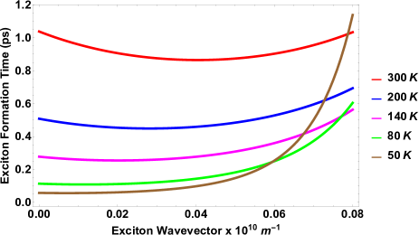
Fig. 1a,b show the calculated values (using Eqs. 7- 16) of the exciton formation times as a function of exciton wavevector with emission of an LO phonon at different electron, hole and exciton temperatures and densities, = = = 1 1011 cm-2 and 5 1011 cm-2. To obtain the results, we assume the temperatures to be the same for excitons and unbound electron-hole pairs. The results indicate that very fast exciton formation times of less than one picosecond time occurs at charge densities of 5 1011 cm-2 and carrier temperatures less than 300 K. These ultrafast sub-picosecond exciton formation times are in agreement with recent experimental findings Ceballos et al. (2016) recorded at room temperatures in the monolayer MoS2. The exciton formation times are increased at the lower carrier densities of 1 1011 cm-2.
The wavevector of exciton states formed due to optical excitation of the ground state of the crystal lies close to zero due to selection rules. The results in Fig. 1a,b show that while excitons are dominantly created at = 0 at low charge carrier temperatures ( 50 K), exciton formation occurs most rapidly at non-zero exciton center-of-mass wavevectors () at higher temperatures ( = 140 K) of the charge carriers. At = 300 K, the shortest exciton formation time occurs at = 0.04 1010 m-1 (about 5.6 meV). The results in Fig. 1a,b indicate that at exciton wavevectors greater than 0.06 1010 m-1, there is a notable increase in the exciton formation times linked to low electron-hole plasma temperatures 80 K. At high carrier temperatures there is likely conversion of newly formed composite bosons such as excitons into fermionic fragment species Thilagam (2013). The inclusion of considerations of the quantum mechanical crossover of excitons into charge carriers at higher plasma temperatures will add to greater accuracy when computing exciton formation times. This currently lies beyond the scope of this study and will be considered in future investigations where the role of the composite structure of excitons in their formation rate will be examined.
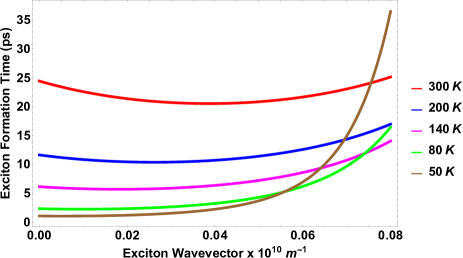
(b) The exciton formation time as a function of the center-of-mass wavevector in the monolayer MoS2 at different temperatures, = = (50 K, 80 K, 140 K, 200 K, 300 K). All other parameters used are the same as specified in (a) with the exception of densities, = = = 5 1011 cm-2.
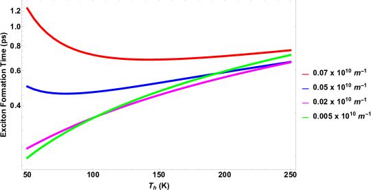
The effect of the variations within the electron-hole plasma temperatures or differences between and on the exciton formation time is illustrated in Fig. 2. The formation times are computed at different exciton center-of-mass wavevectors with the electron temperature fixed at = 250 K, and exciton temperature = 50 K. The charge densities = = = 5 1011 cm-2 and all other parameters used are the same as specified in the caption for Fig. 1. At the larger wavevector = 0.07 1010 m-1 ( 17.1 meV) the formation time is shortest when the hole temperature = 120. With decrease in the center-of-mass wavevector , there is corresponding decrease in the formation time when the hole temperature is allowed to decrease further from the electron temperature. At the low exciton wavevector = 0.005 1010 m-1, the shortest formation time occurs when the difference between and reach the maximum possible value. These results demonstrate the interplay of competitive effects of the hole-phonon and the electron-phonon dynamics on a picosecond time scale which results in a non-monotoinic temperature difference dependence of the exciton formation time.
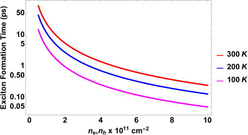
In Fig. 3, the exciton formation time is plotted as a function of the carrier density = at different temperatures, = = (300 K, 200 K, 100 K). The exciton center-of-mass wavevector = 0.03 1010 m-1. All other parameters used are the same as specified in the caption for Fig. 1. Using the numerical values of the formation times, we performed numerical fits using the following relation which involve the carrier concentrations Oh et al. (2000)
| (17) |
where and are fitting parameters. Using the results used to obtain Fig. 3, we get = 20.64 at = = 300 K, = 10.35 at = = 200 K, = 3.56 at = = 100 K and = 1.54 at = = 50 K. The constant 2 irrespective of the electron and hole temperatures. This implies an inverse square-law dependence of the exciton formation time on the electron/hole concentration. Consequently a square-law dependence of the photoluminescence on excitation density is expected to arise in the monolayer MoS2 as well as other monolayer transition metal dichalcogenides.
III Exciton formation times for other exemplary monolayer transition metal dichalcogenides
The theoretical results obtained in this study for MoS2 are expected to be applicable to other low dimensional transition metal dichalcogenides. However subtle variations in the exciton formation times are expected due to differences in the exciton-LO coupling strengths and energies of the LO phonon in the monolayer materials. The bare Fröhlich interaction strengths obtained via ab initio techniques give 334 mev (MoS2), 500 meV (MoSe2), 140 mev (WS2) and 276 meV (WSe2) Sohier et al. (2016), hence the Molybdenum-based TMDCs possess higher exciton-phonon coupling strengths than the Tungsten-based TMDCs. A precise estimate of the exciton binding energy in the monolayer TMDCs is not available, however a range of binding energies (100 to 800 meV) have been reported for the monolayer systems Hanbicki et al. (2015); Olsen et al. (2016); Mak et al. (2010); Cheiwchanchamnangij and Lambrecht (2012); Ugeda et al. (2014); Hill et al. (2015); Choi et al. (2015); Cheiwchanchamnangij and Lambrecht (2012); Komsa and Krasheninnikov (2012); Thilagam (2014a). In order to compare the exciton formation rates between Molybdenum-based TMDCs and Tungsten-based TMDCs, we make use of the effective masses of electron and holes at the energy valleys/peak position given in Ref. Jin et al. (2014) and the Fröhlich interaction strengths and LO phonon energies given in Ref.Sohier et al. (2016). To simplify the numerical analysis, we fix the exciton binding energies at 330 meV for all the TMDCs under investigation. This assumption is not expected to affect the order of magnitude of the exciton formation times, and also to not detract from the analysis of effects of Fröhlich interaction strengths on the formation times.
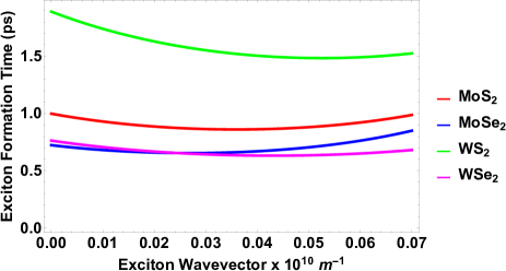
The results in Fig. 4 a, b show that the exciton formation times of the selenide-based dichalcogenides are smaller than the sulphide-based dichalcogenides at = = = 100 K and 300 K (with 0.05 1010 m-1). This is due to the comparatively higher Fröhlich interaction strengths and lower LO phonon energies of monolayer MoSe2 and WSe2. The results in Fig. 4a,b also indicate that excitons in the monolayer WS2 are dominantly created at non-zero center-of-mass wavevectors compared to the other three monolayer dichalcogenide systems. This may be attributed to the comparatively lower effective masses of hole and electron in the monolayer WS2.
It is instructive to compare the exciton formation times in Fig. 4a,b with the radiative lifetimes of zero in-plane momentum excitons in suspended MoS2 monolayer of 0.18 - 0.30 ps at 5 K Wang et al. (2016). The lifetimes of excitons depend linearly on the exciton temperature and increase to the picoseconds range at small temperatures and is larger than 1 ns at the room temperature. This indicates that the exciton formation processes are likely to dominate in the initial period when the TMDCs are optically excited at high exciton temperatures. In the low temperature range (5 K - 20 K), an interplay of competing effects of exciton generation and radiative decay are expected to occur on the sub-picosecond time scale. Environmental parameters such as impurity concentration, exciton density and density of excess charge carriers that affect the stability of low dimensional trions will need to be taken into account in order to accurately model the exciton generation process at the low temperature regime.
The exciton formation scheme adopted in this study has been parameterized by physical quantities such as the exciton density and charge carrier densities. It is not immediately clear whether these parameters can be extracted directly using ab-initio quantum mechanical and time-dependent density functional theory approaches. Computations based on ab-initio techniques are generally numerically intensive and time consuming which are the main challenges in modeling low dimensional material systems. It is expected that improvements in first principles modeling of anisotropic systems may result in more efficient and rewarding approaches to determining the density functions of excitons and charge carriers in future investigations. The Auger process provides a non-radiative decay channel for electron-hole pair recombination, hence this mechanism must be taken into account for accurate predictions of exciton formation times in future studies.
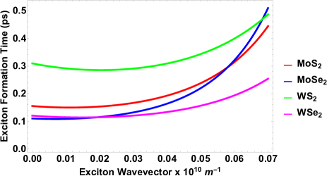
(b) The exciton formation time as a function of the exciton center-of-mass wavevector in common monolayer systems at temperatures, = = = 300 K. All other parameters used are the same as specified in (a) above.
IV Conclusion
Transition metal chalcogenides have emerged as promising materials in which excitons exist as stable quasi-particles with high binding energies and thus play important roles in the optical processes of monolayer TMDCs. The dynamics of excitons in monolayer transition metal dichalcogenides has been extensively studied over the last five years in terms of both theory and applications. However the formation of excitons from free carriers has only been recently measured, and in this work we develop a model within the framework of Fermi’s Golden rule to calculate the formation dynamics of excitons from free carriers. This theoretical study is aimed at providing a fundamental understanding of the exciton generation process in optically excited monolayer transition metal dichalcogenides. We focus on a mechanism by which excitons are generated via the LO (longitudinal optical) phonon-assisted scattering process from free electron-hole pairs in layered structures. The exciton formation time is computed as a function of the exciton center-of-mass wavevector, electron and hole temperatures and densities for known values of the Fröhlich coupling constant, LO phonon energy, lattice temperature and the exciton binding energy. Our results show that the exciton is generated at non-zero wavevectors at higher temperatures ( 120 K) of charge carriers, that is also dependent on the density of the electron and holes. The inverse square-law dependence of the exciton formation time on the density of charge carriers is also demonstrated by the results of this study.
For monolayer MoS2, we obtain exciton formation times on the picosecond time scale at charge densities of 1 1011 cm-2 and carrier temperatures less than 100 K. The exciton formation times decreases to the sub-picosecond time range at higher densities (5 1011 cm-2) and electron-hole plasma temperatures ( 300 K). These ultrafast formation times are in agreement with recent experimental results ( 0.3 ps) for WSe2, MoS2, and MoSe2 Ceballos et al. (2016). Due to the comparatively higher Fröhlich interaction strengths and lower LO phonon energies of monolayer MoSe2 and WSe2, the exciton formation times of the selenide-based dichalcogenides are smaller than the sulphide-based dichalcogenides at = = = 100 K and 300 K (with 0.05 1010 m-1). The results of this study is expected to be useful in understanding the role of the exciton formation process in electroluminescence studies Sundaram et al. (2013); Ye et al. (2014) and exciton-mediated processes in photovoltaic devices Bernardi et al. (2013); Wi et al. (2014); Tsuboi et al. (2015).
References
- Qiu et al. (2016) D. Y. Qiu, F. H. da Jornada, and S. G. Louie, arXiv preprint arXiv:1605.08733 (2016).
- Sahin et al. (2016) H. Sahin, E. Torun, C. Bacaksiz, S. Horzum, J. Kang, R. Senger, and F. Peeters, Wiley Interdisciplinary Reviews: Computational Molecular Science (2016).
- Cudazzo et al. (2016) P. Cudazzo, L. Sponza, C. Giorgetti, L. Reining, F. Sottile, and M. Gatti, Physical review letters 116, 066803 (2016).
- Scharf et al. (2016) B. Scharf, Z. Wang, D. Van Tuan, J. Shan, K. F. Mak, I. Zutic, and H. Dery, arXiv preprint arXiv:1606.07101 (2016).
- Ramasubramaniam (2012) A. Ramasubramaniam, Physical Review B 86, 115409 (2012).
- Ugeda et al. (2014) M. M. Ugeda, A. J. Bradley, S.-F. Shi, H. Felipe, Y. Zhang, D. Y. Qiu, W. Ruan, S.-K. Mo, Z. Hussain, Z.-X. Shen, et al., Nature materials 13, 1091 (2014).
- Wang et al. (2012) Q. H. Wang, K. Kalantar-Zadeh, A. Kis, J. N. Coleman, and M. S. Strano, Nature nanotechnology 7, 699 (2012).
- Mak et al. (2010) K. F. Mak, C. Lee, J. Hone, J. Shan, and T. F. Heinz, Physical Review Letters 105, 136805 (2010).
- Qiu et al. (2013) D. Y. Qiu, H. Felipe, and S. G. Louie, Physical review letters 111, 216805 (2013).
- Splendiani et al. (2010a) A. Splendiani, L. Sun, Y. Zhang, T. Li, J. Kim, C.-Y. Chim, G. Galli, and F. Wang, Nano letters 10, 1271 (2010a).
- Komsa and Krasheninnikov (2012) H.-P. Komsa and A. V. Krasheninnikov, Physical Review B 86, 241201 (2012).
- Kormányos et al. (2013) A. Kormányos, V. Zólyomi, N. D. Drummond, P. Rakyta, G. Burkard, and V. I. Fal’ko, Physical Review B 88, 045416 (2013).
- Ji et al. (2013) Q. Ji, Y. Zhang, T. Gao, Y. Zhang, D. Ma, M. Liu, Y. Chen, X. Qiao, P.-H. Tan, M. Kan, et al., Nano letters 13, 3870 (2013).
- Ghatak et al. (2011) S. Ghatak, A. N. Pal, and A. Ghosh, Acs Nano 5, 7707 (2011).
- Eda and Maier (2013) G. Eda and S. A. Maier, Acs Nano 7, 5660 (2013).
- Berghäuser and Malic (2013) G. Berghäuser and E. Malic, Phys. Rev. B 89, 125309 (2014).
- Molina-Sánchez et al. (2013) A. Molina-Sánchez, D. Sangalli, K. Hummer, A. Marini, and L. Wirtz, Physical Review B 88, 045412 (2013).
- Mai et al. (2013) C. Mai, A. Barrette, Y. Yu, Y. G. Semenov, K. W. Kim, L. Cao, and K. Gundogdu, Nano letters 14, 202 (2013).
- Pospischil et al. (2016b) A. Pospischil, and T. Thomas, Applied Sciences 6, 78 (2016b).
- Plechinger et al. (2012) G. Plechinger, F.-X. Schrettenbrunner, J. Eroms, D. Weiss, C. Schueller, and T. Korn, physica status solidi (RRL)-Rapid Research Letters 6, 126 (2012).
- Gao et al. (2016) W. Gao, Y. H. Lee, R. Jiang, J. Wang, T. Liu, and X. Y. Ling, Advanced Materials 28, 701 (2016).
- Zhu et al. (2016) Y. Zhu, J. Yang, S. Zhang, S. Mokhtar, J. Pei, X. Wang, and Y. Lu, Nanotechnology 27, 135706 (2016).
- Saigal et al. (2016) N. Saigal, V. Sugunakar, and S. Ghosh, Applied Physics Letters 108, 132105 (2016).
- Novoselov et al. (2005) K. Novoselov, D. Jiang, F. Schedin, T. Booth, V. Khotkevich, S. Morozov, and A. Geim, Proceedings of the National Academy of Sciences of the United States of America 102, 10451 (2005).
- Varrla et al. (2015) E. Varrla, C. Backes, K. R. Paton, A. Harvey, Z. Gholamvand, J. McCauley, and J. N. Coleman, Chemistry of Materials 27, 1129 (2015).
- Chen et al. (2015) M. Chen, H. Nam, H. Rokni, S. Wi, J. S. Yoon, P. Chen, K. Kurabayashi, W. Lu, and X. Liang, ACS Nano 9, 8773 (2015).
- Fan et al. (2015) X. Fan, P. Xu, D. Zhou, Y. Sun, Y. C. Li, M. A. T. Nguyen, M. Terrones, and T. E. Mallouk, Nano letters 15, 5956 (2015).
- Li et al. (2016) S.-L. Li, K. Tsukagoshi, E. Orgiu, and P. Samorì, Chemical Society Reviews 45, 118 (2016).
- Perebeinos (2015) V. Perebeinos, Nature nanotechnology 10, 485 (2015).
- Tsai et al. (2013) D.-S. Tsai, K.-K. Liu, D.-H. Lien, M.-L. Tsai, C.-F. Kang, C.-A. Lin, L.-J. Li, and J.-H. He, ACS Nano 7, 3905 (2013).
- Bernardi et al. (2013) M. Bernardi, M. Palummo, and J. C. Grossman, Nano letters 13, 3664 (2013).
- He et al. (2012) Q. He, Z. Zeng, Z. Yin, H. Li, S. Wu, X. Huang, and H. Zhang, Small 8, 2994 (2012).
- Wi et al. (2014) S. Wi, H. Kim, M. Chen, H. Nam, L. J. Guo, E. Meyhofer, and X. Liang, ACS Nano 8, 5270 (2014).
- Bertolazzi et al. (2013) S. Bertolazzi, D. Krasnozhon, and A. Kis, ACS Nano 7, 3246 (2013).
- Yu et al. (2016) C.-H. Yu, M.-L. Fan, K.-C. Yu, V. P.-H. Hu, P. Su, and C.-T. Chuang, IEEE Transactions on Electron Devices 63, 625 (2016).
- Park et al. (2016) M. Park, Y. J. Park, X. Chen, Y.-K. Park, M.-S. Kim, and J.-H. Ahn, Advanced Materials 28, 2555 (2016).
- Radisavljevic et al. (2011) B. Radisavljevic, M. B. Whitwick, and A. Kis, ACS Nano 5, 9934 (2011).
- Lembke et al. (2015) D. Lembke, S. Bertolazzi, and A. Kis, Accounts of chemical research 48, 100 (2015).
- Pospischil et al. (2014) A. Pospischil, M. M. Furchi, and T. Mueller, Nature nanotechnology 9, 257 (2014).
- Zhang et al. (2014) H. Zhang, S. Lu, J. Zheng, J. Du, S. Wen, D. Tang, and K. Loh, Optics express 22, 7249 (2014).
- Yoon et al. (2011) Y. Yoon, K. Ganapathi, and S. Salahuddin, Nano letters 11, 3768 (2011).
- Beck et al. (2000) A. Beck, J. Bednorz, C. Gerber, C. Rossel, and D. Widmer, Applied Physics Letters 77, 139 (2000).
- Ou et al. (2014) J. Z. Ou, A. F. Chrimes, Y. Wang, S.-y. Tang, M. S. Strano, and K. Kalantar-zadeh, Nano letters 14, 857 (2014).
- Shi et al. (2013) H. Shi, R. Yan, S. Bertolazzi, J. Brivio, B. Gao, A. Kis, D. Jena, H. G. Xing, and L. Huang, ACS Nano 7, 1072 (2013).
- Shin et al. (2014) M. J. Shin, D. H. Kim, and D. Lim, Journal of the Korean Physical Society 65, 2077 (2014).
- Ye et al. (2014) Y. Ye, Z. Ye, M. Gharghi, H. Zhu, M. Zhao, Y. Wang, X. Yin, and X. Zhang, Applied Physics Letters 104, 193508 (2014).
- Konabe and Okada (2014) S. Konabe and S. Okada, Physical Review B 90, 155304 (2014).
- Thilagam (2016) A. Thilagam, Journal of Applied Physics 119, 164306 (2016).
- Wang et al. (2015) H. Wang, J. H. Strait, C. Zhang, W. Chan, C. Manolatou, S. Tiwari, and F. Rana, Physical Review B 91, 165411 (2015).
- Mak et al. (2013) K. F. Mak, K. He, C. Lee, G. H. Lee, J. Hone, T. F. Heinz, and J. Shan, Nature materials 12, 207 (2013).
- Berkelbach et al. (2013) T. C. Berkelbach, M. S. Hybertsen, and D. R. Reichman, Physical Review B 88, 045318 (2013).
- Thilagam (1997) A. Thilagam, Physical Review B 55, 7804 (1997).
- Kozawa et al. (2014) D. Kozawa, R. Kumar, A. Carvalho, K. K. Amara, W. Zhao, S. Wang, M. Toh, R. M. Ribeiro, A. C. Neto, K. Matsuda, et al., Nature communications 5 (2014).
- Jones et al. (2013) A. M. Jones, H. Yu, N. J. Ghimire, S. Wu, G. Aivazian, J. S. Ross, B. Zhao, J. Yan, D. G. Mandrus, D. Xiao, et al., Nature nanotechnology 8, 634 (2013).
- Nie et al. (2014) Z. Nie, R. Long, L. Sun, C.-C. Huang, J. Zhang, Q. Xiong, D. W. Hewak, Z. Shen, O. V. Prezhdo, and Z.-H. Loh, ACS Nano 8, 10931 (2014).
- Selig et al. (2016) M. Selig, G. Berghäuser, A. Raja, P. Nagler, C. Schüller, T. F. Heinz, T. Korn, A. Chernikov, E. Malic, and A. Knorr, arXiv preprint arXiv:1605.03359 (2016).
- Mouri et al. (2013a) S. Mouri, Y. Miyauchi, and K. Matsuda, Nano letters 13, 5944 (2013a).
- Siantidis et al. (2001) K. Siantidis, V. Axt, and T. Kuhn, Physical Review B 65, 035303 (2001).
- Ceballos et al. (2016) F. Ceballos, Q. Cui, M. Z. Bellus, and H. Zhao, Nanoscale 8, 11681 (2016).
- Kaasbjerg et al. (2014) K. Kaasbjerg, K. Bhargavi, and S. Kubakaddi, Physical Review B 90, 165436 (2014).
- Kaasbjerg et al. (2012) K. Kaasbjerg, K. S. Thygesen, and K. W. Jacobsen, Physical Review B 85, 115317 (2012).
- Thilagam and Singh (1993) A. Thilagam and J. Singh, Journal of luminescence 55, 11 (1993).
- Oh and Singh (2000) I.-K. Oh and J. Singh, Journal of luminescence 87, 219 (2000).
- Cheiwchanchamnangij and Lambrecht (2012) T. Cheiwchanchamnangij and W. R. Lambrecht, Physical Review B 85, 205302 (2012).
- Hill et al. (2015) H. M. Hill, A. F. Rigosi, C. Roquelet, A. Chernikov, T. C. Berkelbach, D. R. Reichman, M. S. Hybertsen, L. E. Brus, and T. F. Heinz, Nano letters 15, 2992 (2015).
- Thilagam (2014a) A. Thilagam, Journal of Applied Physics 116, 053523 (2014a).
- Oh et al. (2000) I.-K. Oh, J. Singh, A. Thilagam, and A. Vengurlekar, Physical Review B 62, 2045 (2000).
- Cho et al. (2008) J. H. Cho, J. Lee, Y. Xia, B. Kim, Y. He, M. J. Renn, T. P. Lodge, and C. D. Frisbie, Nature materials 7, 900 (2008).
- Mouri et al. (2013b) S. Mouri, Y. Miyauchi, and K. Matsuda, Applied Physics Express 9, 055202 (2016b).
- Sohier et al. (2016) T. Sohier, M. Calandra, and F. Mauri, Phys. Rev. B 94, 085415 (2016).
- Thilagam and Lohe (2006) A. Thilagam and M. Lohe, Journal of Physics: Condensed Matter 18, 3157 (2006).
- Takagahara (1985) T. Takagahara, Physical Review B 31, 6552 (1985).
- Thilagam (2014b) A. Thilagam, Physica B: Condensed Matter 457, 232 (2015b).
- Ivanov et al. (1999) A. Ivanov, P. Littlewood, and H. Haug, Physical Review B 59, 5032 (1999).
- Jin et al. (2014) Z. Jin, X. Li, J. T. Mullen, and K. W. Kim, Phys. Rev. B 90, 045422 (2014).
- Ding et al. (2011) Y. Ding, Y. Wang, J. Ni, L. Shi, S. Shi, and W. Tang, Physica B: Condensed Matter 406, 2254 (2011).
- Thilagam (2013) A. Thilagam, Journal of Mathematical Chemistry 51, 1897 (2013).
- Hanbicki et al. (2015) A. Hanbicki, M. Currie, G. Kioseoglou, A. Friedman, and B. Jonker, Solid State Communications 203, 16 (2015).
- Olsen et al. (2016) T. Olsen, S. Latini, F. Rasmussen, and K. S. Thygesen, Physical review letters 116, 056401 (2016).
- Choi et al. (2015) J.-H. Choi, P. Cui, H. Lan, and Z. Zhang, Physical review letters 115, 066403 (2015).
- Wang et al. (2016) H. Wang, C. Zhang, W. Chan, C. Manolatou, S. Tiwari, and F. Rana, Physical Review B 93, 045407 (2016).
- Sundaram et al. (2013) R. Sundaram, M. Engel, A. Lombardo, R. Krupke, A. Ferrari, P. Avouris, and M. Steiner, Nano letters 13, 1416 (2013).
- Tsuboi et al. (2015) Y. Tsuboi, F. Wang, D. Kozawa, K. Funahashi, S. Mouri, Y. Miyauchi, T. Takenobu, and K. Matsuda, arXiv preprint arXiv:1503.05380 (2015).