Subwavelength Mode Profile Customisation Using Functional Materials
Abstract
An ability to completely customise the mode profile in an electromagnetic waveguide would be a useful ability. Currently, the transverse mode profile in a waveguide might be varied, but this is usually a side effect of design constraints, or for control of dispersion. In contrast, here we show how to control the longitudinal (propagation direction) mode profile on a sub-wavelength scale, but without the need for active solutions such as synthesizing the shape by combining multiple Fourier harmonics. This is done by means of a customised permittivity variation that can be calculated either directly from the desired mode profile, or as inspired by e.g. the range of shapes generated by the Mathieu functions. For applications such as charged particle beam dynamics, requiring field profile shaping in free space, we show that it is possible to achieve this despite the need to cut a channel through the medium.
I Introduction
We show how we can use layered or varying material properties to sculpt an electric field profile along its propagation direction. Here we use sub-wavelength variation as a means of controlling the internal field profile Gratus et al. (2015); Gratus and McCormack (2015), in contrast to the typical uses of layered Russell et al. (1995) or chirped Russell and Birks (1999) 1D photonic crystals, whose focus is primarily on manipulating the band structure, reflectivity, or transmission properties. Up to now most of the work has concentrated on photonic band gaps in photonic crystals, and the transmission or reflection coefficients at various angles or frequencies of an incident wave Joannopoulos et al. (2011). Our method is also distinct from the synthesis of optical waveforms by combining carefully phased harmonics Chan et al. (2011); Cox et al. (2012).
Many possibilities are unlocked by our ability to design field profiles with sub-wavelength customization. We might imagine enhancing ionization in high harmonic generation (HHG, see e.g. Radnor et al. (2008) and citations thereof), where the field profile aims to give a detailed control of the ionized electrons trajectory and recollision. Further, we might create localized peaks in the waveform, so that the concentration of optical power enhances the signal to noise ratio, or gives a larger nonlinear effect. Conversely, flatter profiles could help minimise unwanted nonlinear effects, or better localise the sign transition as happens for a square wave signal. In accelerator applications, there is much interest in controlling the size and/or shape of electron bunches (see e.g. Piot et al. (2011)), or for pre-injection plasma ionisation for laser wakefield acceleration Albert et al. (2014); sculpted electric field profiles are one way of achieving the desired level of control.
Of course, when using customised field profiles to control an electron bunch in an accelerator or synchrotron, we need that field profile to be present in free space. We address this important case using a gap between two slabs of the necessary customised medium, and use CST Studio Suite CST AG simulations of this arrangement to demonstrate that the desired field profile is still present within the slot. A slot also enables probes to be placed to measure the electric field, and can increase the transmission of external fields into the medium.
Here we consider the design of structures that perform this subwavelength field profile shaping. Because we are primarily discussing the basic principles rather than a specific application, we consider a variety of wavelength-scale unit cells designed to be joined together into a long multi-period waveguide structure. The result is a structure in which incident electromagnetic radiation of the correct frequency is transmitted to the far end, and whilst inside the structure it will have its field profile modulated as designed. Although when considering structures made of many unit cells, we restrict ourselves to periodic structures, this is merely for simplicity – if so desired, more complicated profiles could be designed.
In Section II we show how to calculate the permittivity function needed to match a preferred field profile, and in Section II.1 we discuss four specific examples with distinct wave properties and permittivity requirements. Then, in Section III we demonstrate that time domain simulations of multi-period structures do generate the desired field profiles. Finally, in Section IV we present our conlusions.
II The permittivity function
To motivate our scheme we first consider assuming (or guessing) some promising dielectic function , and solving the wave equation for under those conditions, and varying the parameters to search for a suitable field profile. By selecting a simple material variation we could make use of existing solutions; notably repeating two-layer structure would allow us to repurpose work on (e.g.) Bragg reflectors. More interesting would be to assume a sinusoidal variation in permittivity, which has a wave equation that matches that for Mathieu functions111See e.g. http://mathworld.wolfram.com/MathieuFunction.html El Haddad (2016); Gratus et al. (2017). The periodic Mathieu functions depend on two parameters , , where is the -th characteristic value. These give solutions of the differential equation for
| (1) |
It is important to note that is the wavelength of the electric field, which is exactly twice the length of the dielectric modulation. We see this 2:1 ratio between the period of and the period of again below in the designed modes. Sample Mathieu functions, with parameters chosen to give both flat-topped and triangular profiles are shown compared to other similar (but explicitly designed) profiles on fig. 1.
However, although Mathieu functions and the like are powerful sources of inspiration, we prefer to follow a design-lead scheme where we first specify the desired field profile , then use the wave equation to calcuate what the position dependent dielectric properties needs to be. In principle this allows us to directly calculate the material function needed to support almost any electric field profile we might want.
Consider the single frequency transverse mode with , and , together with the permittivity and vacuum permeability . Then Maxwell’s equations, where , give
| (2) |
In principle almost any electric field profile is possible. However, for some field profiles, the solution in (2) requires the presence of negative permittivity, possibly with a very high absolute value; in others is undefined.
To simplify the discussion here we restrict ourselves to modes with odd symmetry about and , and hence even symmetry about where is the desired wavelength222We can also go further and choose our permittivity function so that , and that does not change rapidly. This requires the and that when then , i.e. a point of inflection.. Thus
| (3) |
| (4) |
Thus it is only necessary to specify for . The symmetry requirements imply and . From (4) and (2) one see that has period half that of , and has even symmetry about , i.e. .
It is advantageous for the electric field to be composed of piecewise sections which are either sinusoidal, and hence correspond to constant , or linear, which correspond to .
Following this theoretical design step, we validate our scheme using 3D CST simulations based on a rod-like unit cell oriented along , with a nearly square cross section in and ; the cell shape can be seen in fig. 2. On the boundary we set a perfect magnetic conductor (i.e. ), and on the boundary we have a perfect electric conductor (i.e. ). The boundary conditions are periodic with a phase shift of . We choose these boundary conditions since if we instead used all periodic conditions, then spurious modes with finite or transverse to the variation (in ) would appear.
II.1 Wave Profiles
In this work we confine ourselves to consider only material variation that has a strictly positive-valued permittivity everywhere. In part, this is because materials with negative permittivity are typically strongly dispersive, and so there may be – at the very least – stringent bandwidth limitations. With this constraint, and for some choices of profile, it can be more difficult to construct the permittivity function that supports an electric field with sufficient accuracy.
Nevertheless, by using materials with very low permittivity (epsilon near zero, ENZ), one can construct profiles which are (e.g.) almost flat for a significant proportion of the mode, or which have near constant gradient – both being shown in fig. 1. These profiles were inspired by Mathieu functions of similar appearance, but as we found, that general appearance does not require the specific sinusoidal variation needed for the Mathieu functions themselves. In addition, profiles with strongly localised peaks can be achieved by combining two materials of significantly different permittivities, and if one is prepared to tolerate less precise profiles, it may be possible to construct reasonable flat-top and triangular profiles using only materials with . For brevity, here we will consider only the four representative profiles indicated in table 1. The first three permittivity functions are all step-like, consisting of one high index and one low-index region.
| Shape | Constant | ENZ |
| Flat | ||
| Triangular | ||
| Peak with multiple oscillations | ||
| Peak with two oscillations |
Flat-top wave profile: A flat-topped, or quasi square-wave profile is a familiar waveform, and is often encountered in digital switching circuits, being naturally of a binary (two-level) form. The fast square-wave transitions are ideal for triggering actions at precisely determined intervals; alternatively its periods of near constant field are ideal for applying a (nearly) identical force to each charged particle in a bunch. However, to synthesize this profile directly from its many harmonic components would require a significant effort, especially if attempting to build an optical square wave (see e.g. Chan et al. (2011)). However, using our technique we can sidestep that effort by constructing instead a designer functional material that quite naturally supports such waveforms. We can generate our flat-top wave profile using
| (5) | |||
for , with . We implemented this structure in CST, based on a unit cell with cross section mm, mm, and lengths mm, mm. The slot, when present, was mm wide. Fig. 1 demonstrates that the designed-for field profile is achievable even in a 3D simulation; a 3D visualization is given in fig. 2.
Triangular wave profile: A field profile with a triangular form, just like a square wave or indeed any waveform can be synthesized from its harmonics. In comparison to the square wave in particular, though, the proportion of higher harmonics falls off more rapidly, so any synthesis would in practice be easier. This ramped field profile could also be used to impart a well-managed linear chirp to charged particles in a bunch.
Nevertheless, here we can design a structure which naturally supports triangular waves, which is given by
| (6) | ||||
where , with , and let be the lowest solution to . We implemented this structure in CST, based on the same unit cell as for the flat-top wave; except that when present the slot width was mm. Fig. 1 demonstrates that the designed-for field profile is achievable even in a full 3D simulation. A 3D visualization is given in fig. 2.
A saw-tooth profile could be created in a similar manner by using an ENZ material for the linearly increasing section of the wave, and then a relatively high permittivity segment for the short near-vertical connecting part. Such a wave profile was suggested as a ‘gradient gating’ way of optimising HHG Radnor et al. (2008); the idea being that the initial strong field could ionize a gas atom and accelerate the electron away, before returning to the nucleus to recombine and emit high-energy photons. Subsequent work has focussed on optimising the field profiles on the basis of detailed models of the ionization process Kohler et al. (2012). Given such a wave profile, our method could be used to design a structure to generate it – although tolerating the intense laser pulses used would be a challenge.
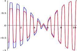
Peaked profile with multiple oscillations: Waveforms with strongly localized peaks can also be useful, particularly where an amplitude and/or intensity threshold is the chosen discriminator. However, just like any wave with distinct or localized features, they have a significant harmonic content and we might therefore prefer not to synthesize them directly. Unfortunately, as we have noted, long intervals of a near-constant electric field in a waveform require very small permittivity values (i.e. the ENZ regime). To avoid this complication, we might replace an idealized near-constant region with many low-amplitude rapid oscillations that are assumed to cycle-average to zero.
In the range there is a small with oscillations, whereas the range provides the desired single large oscillation. The profile is chosen so that , so that
| (7) | ||||
This theoretically designed waveform is shown in fig. 3, along with that resulting from 3D numerical simulations using CST.
Peaked profile with two oscillations: We might also want to generate a peaked profile with only a few minor oscillations per half-period. However, this cannot be achieved with only slabs of constant . Nevertheless, something closer to the design goal can be made if we construct an using two sinusoidal regions and a quadratic Bezier333See e.g. http://mathworld.wolfram.com/BezierCurve.html function to interpolate between them. With from (2), this profile is
| (8) |
For this construction the challenge now becomes that the permittivity becomes very large in a small region; the required can be seen in the inset of fig. 4. Further, even before any difficulties of fabricating an experimental structure are considered, generating numerical results for this is problematic. We therefore split the smooth part of the profile with its extreme values into a set of thin layers, the thinnest layer having (i.e. a refractive index of ). Using this approximate implementation, we can see in fig. 4 the results of using CST to generate a field profile in comparison to the designed-for wave shape – there are significant regions where the match is relatively poor. Nevertheless, the general character of the desired wave profile is achieved, and the important high-field peaks are closely matched.
III Practical Issues
Having first considered very idealized structures that assume an infinite number of periods, we now move to the finite structures of the kind most likely to be built. We have already demonstrated one practical feature of our scheme – the free space field wave profile shaping using a slot. This leaves several important issues to be considered: (i) whether an incident field will penetrate efficiently into the structure for modulation, (ii) the effect of material losses, (iii) and to what extent will the profile shaping persist in the non-idealized case.
First, since the structural periodicity is a good match to the incident wavelength, any device might be expected to act more like a Bragg mirror, with or without a slot. Consequently, we adapted our CST simulations to also treat finite-period structures. The left hand panel of fig. 5 shows a comparision of the bandstructures for a single cell structure, with and without a slot. We can easily see that the character of the bandstructures is preserved and that the slot-induced upward frequency shift is relatively small. This trend was repeated in CST simulations for our other slotted structures. Further, on the right hand panel of fig. 5, we see the transmission spectrum for 10 period structures with and without a slot. As a direct result of our design process, we see that the presence of a slot – and perhaps despite its sub-wavelength width – enhances transmission into the structure.
Second, we need to understand the influence of losses, which is important in the case where metamaterials need to be used to achieve permittivities below the vacuum value – and particularly so for negative values. To estimate the effects of loss we ran a set of time domain CST simulations for slotted ‘flat-top’ structures with 10 repeating elements, with increasing losses. On the available computing hardware (the Lancaster E-MIT distributed computing system) these typically took many hours to run, our longest runs being approximately 20 hours. The losses were specifed by adding an imaginary contribution to the permittivity of each slab in the stack, values which CST used to generate an appropriate response model for its simulations. We primarily investigated three cases, which correspond to no damping, weak damping, and medium damping. The no damping case used a low permittivity slab with and a high permittivity slab with . The weak damping case used a low permittivity slab with and a high permittivity slab with . The medium damping case used a but the same . The scale factor of for each of these was removed in the CST simulations to assist with the numerical calculations, but of course the simulation output then required a compensating rescaling.
The different loss properties of the low and high permittivity slabs mean that the overall loss is some combination of the individual contributions. We therefore obtained the net loss coefficient of the structures from the energy loss rate of our time domain simulations. The simulations showed that for weak losses we had that s-1 and for medium losses we found that s-1. However, as we can see on fig. 6, although the two cases gave different transmission spectra, the qualitative character of the two was preserved. However if we went to “extreme” damping by setting the low permittivity slab to , then this gave a net loss of , which was sufficient to destroy the desired character of our results.
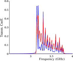
Third, an important feature of these time domain CST simulations was that they also allowed us to extract the mode profiles for specific structures when driven at specified frequencies. Note that in a lossless structure, if the chosen frequency is slightly below the band edge, the incident field will decay with penetration distance inside the structure, although if less than critically damped, the field profile will still have the designed-in modulation (e.g. flat topped), but modulated by a decaying exponential. If the chosen frequency is above the band edge, the designed wave profile will instead be subject to a sinusoidal modulation of the envelope. This means that we want to drive as close to the band edge as possible; but with losses and a finite structure there no longer is a sharp well-defined band edge to choose; however there is a cut-off in the transmission spectrum which on fig. 6 occurs slightly above 3.1GHz. Nevertheless, our time domain simulations do show that field mode profile customization is possible, with results shown on fig. 7. Our expectation is that the envelope modulation could be further minimised by either adjusting the driving frequency, or using a structure with more cells. However, due to the intensive computational requirements, this optimization might be better explored in an experimental setting along with the other practical considerations, rather than in simulation.
IV Conclusions
In summary, we have demonstrated how to achieve considerable freedom to customise electric field profiles, even in free-space, and without resorting to harmonic synthesis. This is achieved by the use of a customised periodic structure with an engineered permittivity profile based on functional materials. The material permittivity function needed can be based either on known solutions, such as specific Mathieu functions, or more generally calculated directly from the wave equation. We have validated our theoretical conception by implementing sample structures in CST, checked that they generate a field profile that matches the design, that the profiling can be achieved in free-space by means of a slotted structure, and that the desired field modes inside the structure can be excited, even in the presence of loss and finite length.
In future work we aim to investigate more realistic models of our structures. The applications in electron beam control that we forsee are in the RF or microwave regime, where sub-wavelength fabrication is relatively easy. Nevertheless, metamaterial fabrication techniques are now routinely being pushed through the THz regime and towards the optical. This is driven in large part by the opportunities made available by transformation optics design Kinsler and McCall (2015): consider for example the infrared Luneburg lens Zhao et al. (2016).
Note that although in several figures we have chosen length scales of millimeters and a frequency regime in the GHz, the general electromagnetic approach we have used applies, or can be rescaled, to either longer or shorter wavelengths. Further, it seems likely that this scheme can be adapted to other fields such as acoustics.
Acknowledgements
The authors are grateful for the support provided by STFC (the Cockcroft Institute ST/G008248/1 and ST/P002056/1) and EPSRC (the Alpha-X project EP/J018171/1 and EP/N028694/1).
References
-
Gratus et al. (2015)
J. Gratus,
M. McCormack,
and R. Letizia,
Proceedings of PIERS 2015 in Prague pp. 675–680 (2015),
http://piers.org/piersproceedings/piers2015PragueProc.php%3Fstart=100. -
Gratus and McCormack (2015)
J. Gratus and
M. McCormack,
J. Opt. 17, 025105 (2015),
arXiv:1503.06131,
doi:10.1088/2040-8978/17/2/025105. -
Russell et al. (1995)
P. S. J. Russell,
T. A. Birks, and
F. D. Lloyd-Lucas, in
Confined Electrons and Photons: New Physics and
Applications, edited by
E. Burstein and
C. Weisbuch
(1995), vol. 340 of
NATO Advanced Science Institutes Series B, pp.
585–633,
conference: NATO Advanced Study Institute on Confined Electrons and Photons - New Physics and Applications,
(Springer, Boston MA)
doi:10.1007/978-1-4615-1963-8%5F19. -
Russell and Birks (1999)
P. S. Russell and
T. A. Birks,
J. Lightwave Techn. 17, 1982 (1999),
doi:10.1109/50.802984. -
Joannopoulos et al. (2011)
J. D. Joannopoulos,
S. G. Johnson,
J. N. Winn, R. D. Meade,
Photonic crystals: molding the flow of light
(Princeton University Press, 2011). -
Chan et al. (2011)
H.-S. Chan,
Z.-M. Hsieh,
W.-H. Liang,
A. H. Kung,
C.-K. Lee,
C.-J. Lai,
R.-P. Pan, and
L.-H. Peng,
Science 331, 1165 (2011),
doi:10.1126/science.1198397. -
Cox et al. (2012)
J. A. Cox,
W. P. Putnam,
A. Sell,
A. Leitenstorfer,
F. X.
Kärtner,
Opt. Lett. 37, 3579 (2012),
doi:10.1364/OL.37.003579. -
Radnor et al. (2008)
S. B. P. Radnor,
L. E. Chipperfield,
P. Kinsler, G. H. C. New,
Phys. Rev. A 77, 033806 (2008),
arXiv:0803.3597,
doi:10.1103/PhysRevA.77.033806. -
Piot et al. (2011)
P. Piot,
Y. E. Sun,
J. G. Power, and
M. Rihaoui,
Phys. Rev. ST Accel. Beams 14, 022801 (2011),
arXiv:1007.4499,
doi:10.1103/PhysRevSTAB.14.022801. -
Albert et al. (2014)
F. Albert,
A. G. R. Thomas,
S. P. D. Mangles,
S. Banerjee,
S. Corde,
A. Flacco,
M. Litos,
D. Neely,
J. Vieira, and
Z. Najmudin,
Plasma Physics and Controlled Fusion 56, 084015 (2014),
doi:10.1088/0741-3335/56/8/084015. -
(11)
CST AG,
CST Studio Suite,
http://www.cst.com/. -
El Haddad (2016)
A. El Haddad,
Optik 127, 1627 (2016),
doi:10.1016/j.ijleo.2015.11.049. -
Gratus et al. (2017)
J. Gratus,
P. Kinsler,
R. Letizia, and
T. Boyd,
Appl. Phys. A 123, 108 (2017),
doi:10.1007/s00339-016-0649-8. -
Kohler et al. (2012)
M. C. Kohler,
T. Pfeifer,
K. Z. Hatsagortsyan,
and C. H.
Keitel, in Advances In Atomic
Molecular and Optical Physics, Volume 61, edited by
E. Arimondo,
P. R. Berman,
and C. C. Lin
(Elsevier, 2012),
vol. 61 of Advances In Atomic
Molecular and Optical Physics, pp. 159–208,
doi:10.1016/B978-0-12-396482-3.00004-1. -
Mandelshtam (2001)
V. A. Mandelshtam,
Progress in Nuclear Magnetic Resonance Spectroscopy 38, 159 (2001),
doi:10.1016/S0079-6565(00)00032-7. -
(16)
S. G. Johnson,
Harminv,
http://ab-initio.mit.edu/wiki/index.php/Harminv. -
Kinsler and McCall (2015)
P. Kinsler and
M. W. McCall,
Photon. Nanostruct. Fundam. Appl. 15, 10 (2015),
doi:10.1016/j.photonics.2015.04.005. -
Zhao et al. (2016)
Y.-Y. Zhao,
Y.-L. Zhang,
M.-L. Zheng,
X.-Z. Dong,
X.-M. Duan, and
Z.-S. Zhao,
Laser and Photonics Reviews 10, 665 (2016),
doi:10.1002/lpor.201600051.