Charge order in an interacting monolayer under transverse bias
Abstract
A monolayer of molecules or quantum dots sandwiched between electrodes can be driven out of equilibrium by the application of a bias voltage between the electrodes. We study charge ordering, i.e., the spontaneous formation of a charge density wave, and the perpendicular current in such a system within a master-equation approach augmented by mean-field and classical Monte Carlo methods. Our approach is suitable for weak tunneling between the monolayer and the electrodes. For a square lattice with nearest-neighbor Coulomb repulsion, we present a comprehensive study of the zero-temperature phases controlled by the on-site energy, the bias voltage, and the degeneracy of the occupied single-site state. One of the most interesting results is the prediction of a conducting charge-density-wave phase that only occurs at a finite bias voltage. We also study the universality classes of the phase transitions towards charge-ordered states at zero and nonzero temperatures. While all transitions at and some at belong to the two-dimensional Ising universality class, we also find an absorbing-to-active phase transition in the symmetric directed percolation (DP2) class at .
pacs:
73.63.-b, 73.23.Hk, 05.70.Ln, 05.50.+qI Introduction
Layers of quantum dots or single molecules sandwiched between conducting electrodes form promising systems for applications as well as for fundamental research. For the past 20 years, experimentalists have investigated the perpendicular current through self-organized layers of quantum dots in semiconductor systems Itskevich et al. (1996); Narihiro et al. (1997); Suzuki et al. (1997); Hapke-Wurst et al. (1999); Belyaev et al. (2001); Hapke-Wurst et al. (2003); Lin and Lee (2003); Pulizzi et al. (2003); Austing et al. (2005); Sun et al. (2006); Vdovin et al. (2007); Swart et al. (2016). These quantum-dot arrays were strongly disordered, though. Molecular layers offer at least two advantages: certain molecules readily form highly ordered self-assembled monolayers on semiconducting or metallic substrates Bigelow et al. (1946); Scheffler et al. (2013); Smykalla et al. (2015); Poirier et al. (1994); Vuillaume et al. (1996); Whitesides and Boncheva (2002) and individual molecules are, in principle, identical. On the other hand, it has proven to be difficult to fabricate a reliable second (top) contact. Novel methods, such as low-energy, indirect-path thermal evaporation Lodha and Janes (2004), rolled-up nanomembranes Prinz et al. (2000); Schmidt and Eberl (2001); Bof Bufon et al. (2014, 2010); *doi:10.1021/nl1022145; *doi:10.1021/nl201773d; *:/content/aip/journal/apl/100/2/10.1063/1.3676269; *doi:10.1021/nl303887b lift-off–float-on techniques Vilan et al. (2000); Vilan and Cahen (2002); Stein et al. (2010), nanotransfer printing Tian et al. (2003); Coll et al. (2009), and transfer of multilayer graphene Wang et al. (2011) have been used to create reasonably homogeneous top contacts to molecular layers. Controlled contacts are a prerequisite for the application of molecular monolayers in electronic devices. Such applications are driven, on the one hand, by the trend to further miniaturization, and, on the other, by the possibility to functionalize the molecules Vuillaume (2010).
Layers of molecules or quantum dots in sandwich structures also constitute model systems for non-equilibrium statistical physics: a bias voltage applied to the electrodes drives the system out of equilibrium. For time-independent bias, the system approaches a stationary state, which is characterized by a stationary current in the direction perpendicular to the monolayer. For non-interacting quantum dots or molecules, the individual entities conduct independently and the theoretical description can fall back on transport theory for single dots or molecules Andergassen et al. (2010); Bruus and Flensberg (2004). The case of interacting dots or molecules is much more interesting in that it combines interactions with driving. Such a system can show spontaneous symmetry breaking, begging the questions whether the corresponding phase transitions belong to a universality class that is known from equilibrium physics or to a genuinely non-equilibrium one Hohenberg and Halperin (1977); Cross and Hohenberg (1993); Hinrichsen (2000); Ódor (2004).
In this paper, we study a relatively simple model in this class, namely, a square array of sites that are either empty or singly occupied due to a high charging energy and that interact through nearest-neighbor Coulomb repulsion. We allow for arbitrary (spin or orbital) degeneracy of the occupied states. The system is sandwiched between electrodes under an applied bias voltage. As we shall see, this non-equilibrium situation can induce spontaneous breaking of translational symmetry Cross and Hohenberg (1993) by the formation of a charge density wave with ordering vector , in which the two checkerboard sublattices have different average occupation. We employ a mean-field approximation in the framework of rate equations to obtain an overview of the possible phases, and classical non-equilibrium Monte Carlo simulations as an unbiased method to study them in more detail.
Our model is similar to the one studied by Kießlich et al. Kießlich et al. (2002); *PhysRevB.68.125331 and by Wetzler et al. Wetzler et al. (2003); *1367-2630-6-1-081, but their systems were relatively small or disordered. Their focus was on small arrays of quantum dots in semiconductor heterostructures, while we are interested in the statistical physics of clean systems in the thermodynamic limit. Leijnse Leijnse (2013) has more recently studied a square array without degeneracy. This work did not address the possibility of charge ordering and did not employ Monte Carlo simulations. A two-dimensional (2D) layer with interactions and hopping was studied within a Keldysh approach by Mitra et al. Mitra et al. (2006). Their interest was in ferromagnetic order in the 2D layer and in the universality class of the non-equilibrium, voltage-driven phase transition.
II Model and methods
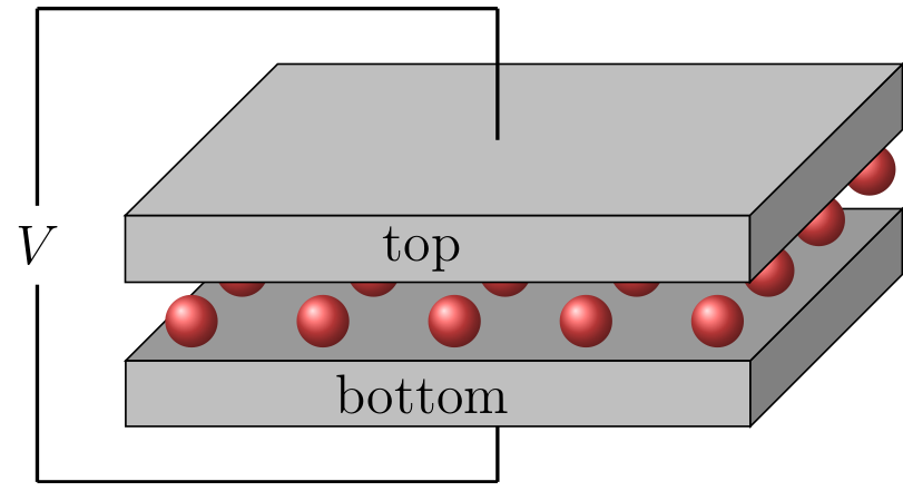
Our model consists of a 2D square lattice of quantum dots or molecules sandwiched between two conducting electrodes, as sketched in Fig. 1. The Hamiltonian consists of the three terms
| (1) | ||||
| (2) | ||||
| (3) |
where is the single-particle energy of the individual dots or molecules, is the on-site Coulomb interaction, is the nearest-neighbor Coulomb interaction, is the dispersion of electrons in the electrodes, is the chemical potential in electrode , and is the tunneling amplitude between the electrodes and the monolayer. For simplicity, the tunneling amplitude and the density of states of the electrodes are assumed to be constant. is the electronic annihilation operator for a state in the monolayer at site with quantum numbers , which could include the spin but, importantly, may also include an orbital index, and is the corresponding number operator. is the annihilation operator for a state with spin and momentum in electrode . We use as our unit of energy and measure relative to the chemical potential in equilibrium. We consider the limit so that each site can only be empty or singly occupied. The voltage drop is assumed to be symmetric and the applied bias voltage is given by .
The Hamiltonian for the layer, Eq. (1), does not contain intralayer hopping. For quantum dots, this situation is easily realized by making the separation between dots sufficiently large. On the other hand, molecular layers are typically closely packed. It is nevertheless possible to reduce the overlap between the relevant orbitals of neighboring molecules by choosing appropriate side groups. In the absence of wave-function overlap and tunneling within the layer, the exchange interaction between different sites also vanishes and we are left with the direct Coulomb interaction in Eq. (1). The spin thus only enters by causing a twofold degeneracy. From a theoretical perspective, inclusion of intralayer hopping would transform the system into an extended Hubbard model out of equilibrium, a much more difficult problem. The methods we will discuss below rely on the decomposition of the many-particle dynamics into single-site processes (coupled by their dependence on the occupation of neighboring sites). This would not be possible in the presence of intralayer hopping, which would instead require us to consider the many-body eigenstates of an extended Hubbard model.
The degeneracy of the occupied states, i.e., the number of possible realizations of an occupied site, is denoted by , while we assume the unoccupied state to be non-degenerate. Hence, for lattice sites ( is the linear size of the system), there are possible many-particle states. It is, however, advantageous to view the occupied states as a single one and include the degeneracy factor explicitly in the equations. The case of a single orbital per site, spin , and vanishing magnetic field corresponds to . A strong magnetic field that shifts one spin orientation up to high energies would lead to . Orbital degeneracies and effective degeneracies due to vibrational modes Bolvin and Kahn (1995a); *Bolvin1995355; A. Bousseksou et al. (1995); Yokoyama et al. (1998) and local magnetic moments can result in larger values of . Degeneracies of both the occupied and the unoccupied states are easily included and lead to the same results, except for overall constant factors, where is now the ratio of the degeneracies of occupied and unoccupied states. A degeneracy of what we call the unoccupied state is naturally realized if the transition is not between an empty and a singly occupied orbital but between a singly occupied and a doubly occupied orbital. We conclude that it is meaningful to allow to take any positive real value.
II.1 Master equation
For weak tunneling to the electrodes but strong interactions and , the master-equation formalism is most suitable Bruus and Flensberg (2004); Breuer and Petruccione (2007); Timm (2008); Andergassen et al. (2010). The master equation is the equation of motion for the reduced density operator of the monolayer, , where is the density operator of the whole system. In the limit of weak tunneling, a perturbative expansion in the tunneling amplitude can be employed. The sequential-tunneling approximation is obtained by truncating this expansion after the second order. Furthermore, we make the standard assumption that the monolayer and the electrodes are in a product state with the electrodes in separate equilibrium at an early time . By suitably organizing the expansion (or, alternatively, by a Markov assumption), we can make the resulting master equation local in time Breuer and Petruccione (2007); Timm (2008). The result is the Wangsness-Bloch-Redfield master equation Wangsness and Bloch (1953); Bloch (1957); Redfield (1965),
| (4) |
where describes the initial equilibrium state of the electrodes and we have set . We focus on the stationary state, which is obtained by setting . The result is a linear algebraic equation for .
We employ the basis of occupation-number states in real space, i.e., of eigenstates of all number operators . The corresponding eigenvalues are denoted by . These states are also eigenstates of . In this work, we assume that the stationary reduced density operator is diagonal in this basis, i.e., we will neglect all coherences. In the following, we discuss the conditions for this assumption to be valid.
First of all, coherences between states with different total particle numbers , dephase nearly instantaneously due to superselection rules Wick et al. (1952); *PhysRevD.1.3267; Zurek (1982); Giulini et al. (1995). Such coherences are also seen to decouple from the diagonal components of (i.e., the probabilities) and from the coherences between states with the same total particle number in Eq. (4). Coherences of the latter type do couple to the diagonal components and are generated with time even if they are not present in the initial state. The relevant processes involve the tunneling of an electron out of site of the molecular layer into a typically adjacent site in electrode and then back out of a site in the electrode into site in the molecular layer (or in the opposite temporal order). Mathematically, they are controlled by the lesser and greater Green functions of lead electrons, which appear in the integral term of the master equation (4) Timm (2008). In a clean system, the Green functions for states close to the chemical potential decay in real space as , where is the distance between points and in the electrode. This means that the terms generating non-local coherences are small if the distance between neighboring molecules—or more precisely between the points in the electrodes connected to neighboring molecules by tunneling—is large compared to the Fermi wavelength in the electrodes. Moreover, in the presence of disorder in the leads, the Green functions are additionally cut off at the scale of the mean free path . We conclude that non-local coherences can be neglected if the separation between neighboring molecules is large compared to the Fermi wavelength or to the mean free path in the electrodes.
This leaves the possibility of coherences between states that only differ by the local quantum numbers . Let us first consider the case that in Eq. (1) only refers to the z-component of the real spin. It is easy to check that coherences between spin states decouple from the diagonal components if the full Hamiltonian conserves spin. This means that such coherences are not generated if they are not present in the initial state and, moreover, decay to zero if there is any arbitrarily weak spin relaxation. This conclusion carries over to the case with containing additional (orbital) degrees of freedom: coherences can be neglected if conserves the full set of quantum numbers . This for example applies to a model involving molecules with and (or and ) orbitals where the interface is the xy plane. Tunneling only occurs to lead orbitals with the same mirror symmetries with regard to the xz and yz planes so that the pseudo-spin distinguishing between the two orbitals is conserved, in addition to the real spin.
If coherences are neglected, the master equation simplifies to rate equations for the probabilities of the many-body states of the monolayer:
| (5) |
In the sequential-tunneling approximation, the rates take the form Elste and Timm (2005); Timm (2008, 2011)
| (6) |
with
| (7) |
where is the density of states per electrode and spin, is the Fermi function , and . We have dropped the index because the rates do not depend on it and the degeneracy is already included explicitly in the in-tunneling rates. Furthermore, we have used that sequential tunneling only connects many-body states , that differ by a single electron at a single site and only depends on the local energy contributions and , where is the number of occupied sites neighboring .
It is easy to check that in the case of , i.e., for , the rates satisfy detailed balance so that the system relaxes into its equilibrium state at the temperature of the electrodes. For and , our system is equivalent to an Ising model in equilibrium. The role of the Ising magnetic field is played by the on-site energy . The degeneracy can be absorbed into this magnetic field as a temperature-dependent term, as we discuss below.
Our model satisfies a particle-hole symmetry. The symmetry operation consists of interchanging in-tunneling and out-tunneling processes and mapping the on-site energy according to . For , the degeneracy of the unoccupied state becomes after the mapping. At the level of the rate equations, this is equivalent to setting the degeneracy of the occupied state to and multiplying by .
The staggered magnetization of an antiferromagnetic Ising model maps to , where and are the occupation numbers of any site on the checkerboard sublattices and , respectively. The brackets denote the statistical average, over space and time, in the stationary state. Due to , we have . We call the checkerboard order parameter from now on. The corresponding susceptibility is
| (8) |
Furthermore, we denote the total electron number in the molecular layer by , the number of nearest-neighbor bonds of type , corresponding to empty-empty, empty-occupied, etc., by , and the associated concentrations by and . Lastly, the average current per site from the monolayer into the electrode is given by
| (9) |
where () is the total electron number in the monolayer in the initial (final) state.
II.2 Mean-field approximation versus Monte Carlo simulations
We solve the rate equations (5) employing two complementary methods. First, we apply a mean-field approximation at the level of probabilities (mean-field master equation, MFME). Specifically, we trace out all sites except for a single site in the rate equations (5). The resulting probability for site having the occupation number is , where represents a many-body state of the whole layer in the occupation-number basis. The rate equations then take the form , where the right-hand side still depends on the full configuration. The main approximation then consists of the product ansatz in . This approximation leads to coupled equations for the single-site probabilities for all sites . Using , these are independent probabilities. To simplify the problem further, we only consider specific spatial variations of the probabilities . Since we are interested in checkerboard order, we assume to be the same for all on the same checkerboard sublattice or , i.e., for and for . This only permits uniform and checkerboard-ordered solutions, where the uniform state corresponds to . Since for , we have now reduced the problem to finding two unknowns and . The product ansatz constitutes a mean-field-type approximation since it replaces the spatial correlations included in by much simpler ones that only depend on the averaged occupation on each sublattice. This approximation goes beyond a Hartree approximation, which would replace the nearest-neighbor Coulomb interaction by the interaction with the average charge density. Here, we retain the information that the sites are always either occupied or unoccupied.
The resulting equation of motion for the probability of a site on sublattice , here denoted as site , having the occupation reads as
| (10) |
In deriving this equation, we have used that under sequential tunneling only the occupation number of a single site changes. The transition rate for this process depends on whether an electron tunnels in or out and on the number of occupied neighboring sites. We can thus parametrize the rates by the initial and final occupation numbers, and , respectively, and the number of occupied neighboring sites on the square lattice, enumerated by . In Eq. (10), for sublattice since the neighboring sites are always on the other sublattice. Here and in the following, we use as a short-hand notation for the full many-body state , which highlights the quantities that affect the sequential tunneling at site . Stationary states are fixed points, which are obtained by setting the time derivatives to zero. We solve the equations numerically, discarding any unstable fixed points. We note that this procedure is different from the one used in Ref. Leijnse (2013), which is formulated in terms of the conditional occupation probabilities of the sites, depending on the occupation of their neighbors.
Second and foremost, we use Monte Carlo simulations. While they are numerically more expensive, they have the advantage of being free from approximations beyond those made in the derivation of the sequential-tunneling rate equations (5), apart from finite-size effects. Moreover, the solutions are not restricted to uniform or checkerboard order. As the system size is finite, we have to evaluate the average instead of . We consider linear system sizes between 16 and 16 384 and periodic boundary conditions.
The straightforward algorithm for local updates is the following: Randomly choose a site . If this site is initially occupied (unoccupied) the only possible transition is to the unoccupied (occupied) state. Calculate the rate for this transition from Eqs. (6)) and (7); the result depends on the occupations of the neighboring sites. Accept the transition with the probability , where is the maximum possible rate.
This algorithm is highly inefficient if the rate chosen as described above often turns out to be small compared to since then many Monte Carlo steps are rejected. Hence, we instead employ the rejection-free update scheme described in the following. First, note that there are only distinct local updates in sequential tunneling, which are enumerated by the initial occupation and the number of occupied neighbors, . We first randomly select one of the 10 update types with the proper branching fraction , which is determined from the total rates of processes of each of the types, , where enumerates the sites of the system. These quantities are easily updated in each Monte Carlo step. Then we randomly choose a site with occupation and occupied neighbors. This step is rejection free since the program keeps lists of all sites that are in each of the 10 states . Lastly, we update this site and advance the simulation time by the average waiting time 111Kinetic simulations would require us to advance the simulation time by an exponentially distributed time with this mean. However, for the long-time limit we are interested in, both prescriptions give the same results.. This algorithm is related to the one introduced by Bortz et al. Bortz et al. (1975) and independently by Gillespie Gillespie (1976); *doi:10.1021/j100540a008, and further improved by Schulze Schulze (2002). We measure all times in units of , which is the average waiting time between two tunneling events at a single site if the transition is inside the bias window and and . To our knowledge, more efficient update algorithms, such as cluster updates Swendsen and Wang (1986); Wolff (1989), do not exist for the rates in Eq. (6), which do not satisfy detailed balance.
III Results for zero temperature
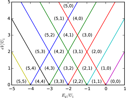

In the limit of zero temperature, the Fermi distribution becomes a step function and thus the rates change discontinuously. Consequently, the stationary state is the same for all values of and within each of the regions defined in Fig. 2. This allows us to give a complete discussion of all possible stationary states. The regions are labeled by the numbers of transition energies below the chemical potentials of the two electrodes. As an example, Fig. 3 shows the relevant energies for the region : four transitions lie below the chemical potential of the top electrode but only one transition lies below the chemical potential of the bottom electrode.
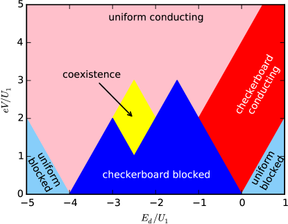
To get an overview, we present in Fig. 4 the MFME phase diagram for the case . We find all possible combinations of phases with and without checkerboard charge order and with and without a charge current through the monolayer. In the presence of checkerboard order, the MFME has two stationary solutions, which are related by interchanging the two sublattices. In the region labeled “coexistence,” the stationary MFME has both checkerboard blocked and uniform conducting solutions. In the following, we discuss each phase based on rigorous results and Monte Carlo simulations.
III.1 Uniform conducting phase at large bias
For fixed on-site energy and sufficiently high bias voltage , the system is always in the region (see Fig. 2). In this regime, an analytical solution of the rate equations (5) is possible. Since the in-tunneling and out-tunneling rates are independent of the occupation numbers of the neighboring sites, the dynamics of the individual sites is decoupled. In the stationary state, the probabilities of a site being occupied or unoccupied are and , respectively. These are the same values one finds for the equilibrium () state in the limit . The average current per site is . The system is clearly in the uniform conducting phase. The solution of the rate equations (5) is given by the product of the aforementioned single-site probabilities since the sites are decoupled.
III.2 Quasi-equilibrium, blocked phases
All regions connected to the zero-bias line, i.e., the regions and in Fig. 2, can be mapped onto an equilibrium Ising-type model with degeneracy of one of the states and an applied magnetic field, as we show in the following. The equilibrium Ising model with has of course been investigated thoroughly Pathria and Beale (2011); Müller-Hartmann and Zittartz (1977); Mahan and Claro (1977). The mapping between our monolayer Hamiltonian and the Ising Hamiltonian
| (11) |
reads as
| (12) | ||||
| (13) | ||||
| (14) |
The state has degeneracy .
We first consider the regions , which contain parts of the line . Recall that the stationary state is the same throughout each region. It is thus sufficient to investigate the case , which corresponds to the model in equilibrium, in the limit . But this state is just the ground state of . For , this is the fully occupied state. For , there are two degenerate ground states with checkerboard charge order with one sublattice occupied and the other unoccupied. Finally, for the ground state is completely empty. The degeneracy is irrelevant in these cases since the energy of the microstates does not depend on it. The corresponding currents [Eq. (9)] vanish in all these regions since all transition rates out of the respective ground states go to zero for 222One might ask whether the rate equations really describe relaxation into these ground states. This is the case if we set and then take the limit since the system is ergodic for any .
Next, we turn to the regions , which touch the line at a single point. While the stationary state is still the same throughout each of these regions, the equilibrium state now lies at a corner of the region, which may be distinct from its interior. These corner points at have fine-tuned values of (see Fig. 2), and correspond to one transition energy being resonant with the chemical potential, which is the same for both electrodes. One can see from Eq. (7) that the rates in the interior, i.e., for , and at the corner, i.e., for , have the same limit for . This result relies on the symmetric coupling to the electrodes: for , the Fermi functions involving the resonant transition approach for both electrodes in the limit , whereas for , one of them approaches unity and the other zero. Since for symmetric coupling only their sum enters, the results are the same. For the regions , , and , the stationary states are thus identical to the ground states for fine-tuned on-site energies , , and , respectively. However, these ground states are not different from the rest of the range : they are the two states with checkerboard order. The current again vanishes, by the same argument as above. The regions and are special in that their corner points at lie right on the transition between different ground states. We will investigate these cases in Sec. III.3.
In summary, in the regions , , , , , , and we find checkerboard charge order and vanishing current, in agreement with the MFME phase diagram in Fig. 4. This phase can be understood in terms of Coulomb blockade due to the nearest-neighbor repulsion . In the region , the sites are fully occupied and the current vanishes. This is the Coulomb-blockade regime due to the on-site repulsion . Finally, in the region we find an empty lattice and vanishing current.
III.3 Degeneracy-driven phase transitions in the conducting phases
We now consider the regions , , , and and their particle-hole-symmetry partners , , , and in Fig. 2. The regions and are interesting since the discussion in Sec. III.2 suggests that their stationary states inherit properties from an equilibrium Ising model fine tuned to its critical point. Moreover, for the region [as well as ] the MFME for predicts a state with checkerboard charge order that is nevertheless conducting (see Fig. 4). On the other hand, the state in region is uniform and conducting, according to the MFME. Since the region with degeneracy is equivalent to the region with degeneracy by a particle-hole transformation, the MFME results imply the existence of a phase transition between uniform and checkerboard states as a function of . Indeed, by determining the stationary state of the MFME for various , we find the critical degeneracy . It is then interesting to characterize this phase transition without making a mean-field approximation. In particular, we want to determine its universality class.
Before turning to the simulations, we first present an analytical estimate for the critical degeneracy for the region . The critical value for the region is then just . As noted in Sec. III.2, in the limit the rates in the interior of region are the same as at the corner point , . The critical value can be related to the critical magnetic field of an antiferromagnetic Ising model. We set and consider the partition function , where is the energy of microstate and is the number of occupied sites in this microstate. The energy is given by , where is the number of bonds between two occupied neighboring sites in microstate . The partition function can be written as
| (15) |
According to Eq. (14), the Ising magnetic field is now . At the corner point of the region , we have . The equivalent Ising model shows a phase transition between checkerboard and uniform order as a function of magnetic field. The critical field is determined by the temperature and the coupling constant . Taking into account that is negative for small , we can then write the critical degeneracy as
| (16) |
This expression is exact but, to the best of our knowledge, the analytical form of the function is not known Müller-Hartmann and Zittartz (1977); Blöte and den Nijs (1988). The conjectured low-temperature expansion proposed by Müller-Hartmann and Zittartz Müller-Hartmann and Zittartz (1977), , gives .
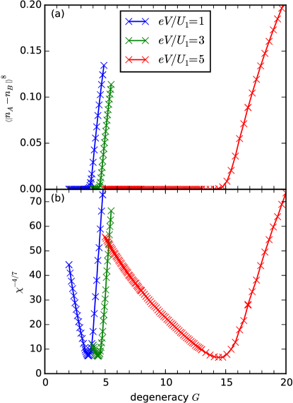
The above discussion is based on the mapping to an equilibrium Ising model. This is not possible for the regions and , which should, however, be physically similar to since all out-tunneling transitions are energetically possible while only some in-tunneling transitions are allowed. [The region will be discussed below.] We have performed Monte Carlo simulations to study the degeneracy-driven transition in these regions. Figure 5 shows the checkerboard order parameter raised to the power and the corresponding susceptibility to the power . For all three regions , , and , we find a transition to checkerboard order for increasing degeneracy . The critical degeneracy for the region is slightly smaller than the value of based on the low-temperature expansion of Ref. Müller-Hartmann and Zittartz (1977). On the other hand, the MFME prediction, , is clearly much too small. Indeed, for the case of with pure spin degeneracy, our simulations do not find checkerboard order in any conducting region, in contrast to the MFME phase diagram in Fig. 4.
Figure 5 shows some finite-size effects, in particular in the susceptibility. Nevertheless, the transitions in the regions , , and are consistent with critical exponents of for the order parameter and for the susceptibility, respectively, and thus with 2D Ising critical behavior Pathria and Beale (2011). The non-equilibrium transition is indeed expected to belong to the classical 2D Ising universality class based on the arguments of Ref. Mitra et al. (2006): integrating out the microscopic degrees of freedom, one obtains a description in terms of a classical field coupled to noise. Generically, the spectrum of this noise is nonzero in the zero-frequency limit, which corresponds to the Ising universality class (“model A” in the terminology of Hohenberg and Halperin Hohenberg and Halperin (1977)). Newer works show that this is indeed true for a scalar (Ising) model, such as ours, but not for multi-component order parameters Sieberer et al. (2013); *PhysRevB.89.134310.
Moreover, increases with increasing bias voltage , i.e., from region to and even more to . This dependence can be understood as follows: for a perfect checkerboard-ordered state, a current flows through the occupied sublattice, as the out-tunneling transition is in the bias window. In contrast, the in-tunneling transition needed to fill a site on the empty sublattice, i.e., to create an occupied defect, is forbidden, except when there are enough empty defects at the surrounding sites on the occupied sublattice. Raising the bias voltage lowers the required number of empty defects and thus makes it easier to destroy the checkerboard order. On the other hand, raising increases the in-tunneling rate for filling an empty site, i.e., for removing an empty defect, which stabilizes the order 333Raising also increases the rate for creating an occupied defect on the empty sublattice, which destabilizes the order, but for this to happen more than one empty defect at neighboring sites is needed, which makes the overall creation rate of such defects much smaller than the overall rate for removing empty defects..
In the region , checkerboard order is even more strongly destabilized than in the previous cases since an occupied defect on the empty sublattice is possible as soon as one empty defect on the occupied sublattice exists. Furthermore, the average concentration of empty defects on the occupied sublattice is high since the out-tunneling transition is in the bias window. This concentration is suppressed by a large but at the same time the creation rate for occupied defects neighboring an empty defect is enhanced. The latter effect evidently prevents charge order even at large . Our simulations do not show any sign of a transition for up to .
The regions , , , and are related to the regions , , , and , respectively, by interchanging empty and occupied states and replacing by . This means that degeneracy-driven transitions in regions , , and take place at critical values , which correspond to higher degeneracy of the empty state compared to the occupied state of a single site (see the discussion of in Sec. II).
III.4 Absorbing phase transitions
We now turn to the three diamond-shaped regions highest in the bias voltage, i.e., regions , its particle-hole-symmetry partner , and in Fig. 2. In all three and indeed in all regions with and , the rates for the transitions and both vanish (for the notation , see Fig. 3). Consequently, there are no allowed transitions out of the perfect checkerboard states. This is the defining property of absorbing states Hinrichsen (2000); Ódor (2004). Absorbing states are necessarily stationary, but for an infinite system it is possible that the stationary state approached from nearly all (namely, all except for a fraction that vanishes in the thermodynamic limit) initial states is not one of the absorbing states. Such a non-absorbing stationary state is called active. If an active state only exists in part of the parameter range, then an absorbing-to-active phase transition has to occur Hinrichsen (2000); Ódor (2004).
Our Monte Carlo simulations suggest that the stationary state in regions and is an absorbing checkerboard state for but is a uniform, and thus active, state in the region . However, the results have to be analyzed with care since for any finite system the simulation will eventually end up in one of the absorbing states, possibly after a very long time.
To check that the regions really lie on different sides of an absorbing phase transition, it is desirably to tune continuously through the purported transition. In addition, this would allow us to determine its universality class. However, the naive idea of fixing the temperature to a small nonzero value and tuning the bias voltage does not work since at the transitions out of the perfect checkerboard states occur with nonzero rates so that these states are no longer absorbing. Instead, we define , where is a bias voltage on the boundary between the regions and for a suitably chosen . The boundary between regions and is analogous. The rates and , which make the checkerboard state non-absorbing, are then proportional to the Fermi function . These rates are tuned to zero by letting . On the other hand, the rates and are proportional to and are kept constant by taking while keeping fixed.
Now, being able to tune our system continuously by changing , we use a dynamical-scaling analysis Ferrell et al. (1967); *FERRELL1968565; Halperin and Hohenberg (1969); Grassberger and de la Torre (1979); Muñoz et al. (1997); Hinrichsen (2000) to clarify the occurring phases and transitions. Two standard critical exponents of an absorbing phase transition are defined by the scaling relations Muñoz et al. (1997); Hinrichsen (2000)
| (17) | ||||
| (18) |
for large times . They pertain to a system prepared in an initial state that differs from an absorbing (checkerboard) states by a localized defect. is the survival probability, i.e., the probability that the system does not reach an absorbing state until the time , and is the density of active sites Hinrichsen (2000), which in our model correspond to empty-empty and occupied-occupied nearest-neighbor bonds. Note that both exponents are free from finite-size effects since in our simulations the lattice was always larger than any grown cluster of active sites.
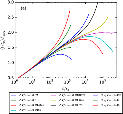
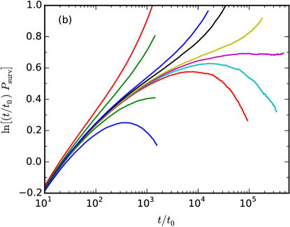
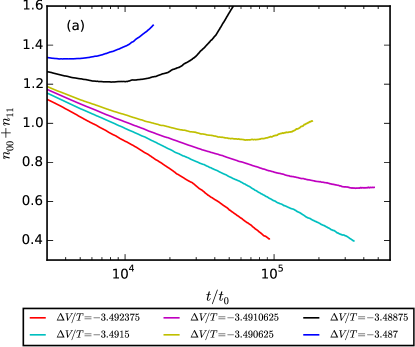

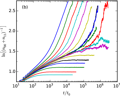
We concentrate on simulations for . Figure 6 shows results for . Since the exponent is close to unity, we have plotted multiplied by . Figure 7 shows results for . We find a clear transition at that agrees with the 2D symmetric directed-percolation universality class (DP2) Hinrichsen (2000); Lee and Vojta (2011); Hinrichsen (1997). Dornic et al. Dornic et al. (2001) conjecture that there is a mapping between the DP2 universality class and a generalized voter model. The latter has an upper critical dimension of two so that one expects mean-field exponents and with logarithmic corrections Lee and Vojta (2011); Hinrichsen (1997). Previous work supports either mean-field behavior with logarithmic corrections or exponents rather close to the mean-field ones Lee and Vojta (2011); Hinrichsen (1997), where the best estimate is and Lee and Vojta (2011).
While our focus is not on this debate, we briefly comment on the critical behavior. If followed mean-field scaling with logarithmic corrections, Fig. 6(a) would show a straight line for large , at the critical value of . If instead satisfied the power law Eq. (17), Fig. 6(b) would show a straight line. Similarly, Fig. 7(a) [Fig. 7(b)] would show a straight line at the critical if showed mean-field scaling with logarithmic corrections (power-law scaling). While in Fig. 6 appears to depend logarithmically on for small [note the straight line in Fig. 7(a)], crosses over to pure mean-field scaling with exponent and without logarithmic corrections for (horizontal line in both panels for ). On the other hand, the scaling of shown in Fig. 7 does not clearly discriminate between the two scaling forms. The data for are not consistent with the mean-field exponent without logarithmic corrections, i.e., with , for , unlike in Fig. 6. We suggest that either the large- scaling regime has not been reached in our simulations or the corrections are more complicated than a simple logarithm .
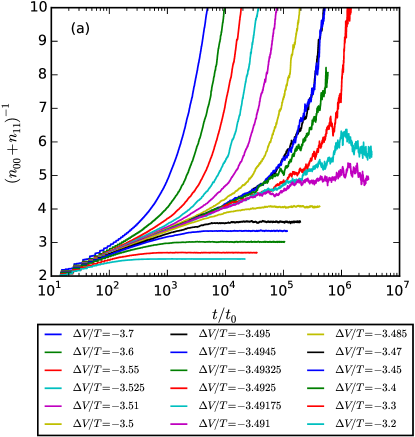
To check the DP2 universality further, we have investigated the time evolution of the concentration of active sites, i.e., of empty-empty and occupied-occupied bonds, when we start from a completely empty or completely occupied lattice, in which all bonds are active. In this case, the mean-field plus logarithmic form of the scaling relation at criticality reads as
| (19) |
whereas the power-law form is
| (20) |
where the best estimate is Lee and Vojta (2011). Our results are presented in Fig. 8. Figure 8(a) [8(b)] would show a straight line at the critical if satisfied mean-field plus logarithmic (power-law) scaling. The data agree better with mean-field scaling with logarithmic corrections for smaller but do not exclude a crossover to power-law scaling at larger times.
In any case, while we cannot resolve the critical behavior, the transition between regions and shows clear characteristics of the 2D DP2 universality class. This is reasonable since a key feature of DP2 is the existence of two symmetry-related absorbing states. Our model obviously has two absorbing checkerboard states that are related by a lattice translation. The DP2 character of the transition supports our conclusion that the system in region is in the active, uniform state, whereas in region it is in the absorbing, checkerboard state. It is interesting that we find a DP2 transition in view of the expectation that the non-equilibrium phase transitions of our model are generically of Ising type Mitra et al. (2006); Sieberer et al. (2013); *PhysRevB.89.134310. We conjecture that this is made possible by the fine tuning inherent in taking and to zero with fixed.
The question arises as to whether the system in the regions , , and can be driven across the DP2 absorbing phase transition by varying . Increasing favors occupied over empty sites. We would thus expect it to destabilize checkerboard order in favor of a uniform state with occupancy close to unity. Since region is in the active phase even for we do not expect the active phase to be destroyed for any . Indeed, we have not found any sign of checkerboard order for values up to .
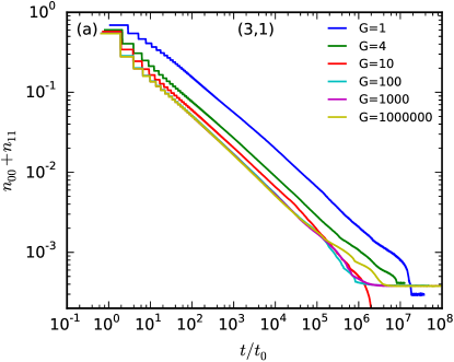
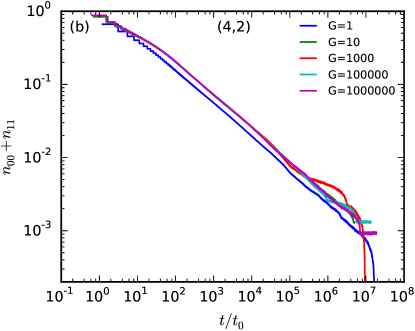
We now turn to the regions and , in which a DP2 transition as a function of might occur. We present simulation results for the surviving concentration of active bonds for a fully occupied (hence, active) starting configuration in Fig. 9. There is no indication of a phase transition for up to . Note that the time evolutions shown in Fig. 9 sometimes get trapped in a seemingly stationary state with nonzero active sites. These states consist of an even number of straight domain walls of the checkerboard order spanning the finite, periodic system. These domain walls are very long lived under local updates since their annihilation requires them to first deform and reconnect. They clearly would not be possible in an infinite system. Thus we conclude that the regions and are in the absorbing phase for all . In particular, the coexistence regime found in the MFME phase diagram in Fig. 4 does not exist, only the checkerboard blocked phase is stable here. This general result is further supported by the power-law decay of with time, in the limit of large but before finite-size effects occur, with an exponent of approximately . This behavior was previously interpreted as being characteristic for the absorbing regime Dornic et al. (2001).
III.5 Phase diagram, occupation, and current

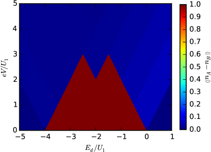
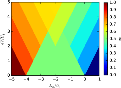

In the previous subsections, we have discussed the stationary state at for all the regions in Fig. 2. The results are summarized in the phase diagram in Fig. 10, which partially anticipates results for the current that are presented below. We mention in passing that, although the simulations are not restricted to uniform and checkerboard-ordered phases, we did not find any other type of charge order. One of the most intriguing results is the possibility of bias-induced charge order: consider for example an on-site energy . If the degeneracy is sufficiently large and we increase the bias voltage starting from zero, the system is initially in a uniform blocked phase with all sites empty. But at it enters a conducting phase with checkerboard charge order, see Sec. III.3. At a higher bias, there is a second transition towards a uniform conducting phase.
While the applied bias voltage is easily varied, this is not the case for the on-site energy . One could, however, prepare series of devices with different on-site energies. In molecular monolayers, one can tune by interchanging side groups, as studied experimentally in Ref. Venkataraman et al. (2007) and theoretically in Ref. Mowbray et al. (2008). Tuning in situ is more difficult. Note that tuning and is equivalent to changing the potential drops between the molecules and the two electrodes independently. This could be done by asymmetrically changing the molecule-electrode distances: if the molecules are covalently bound to one electrode but only van der Waals-coupled to the other, changing the electrode-electrode separation would have the desired effect. This would of course also change the tunneling amplitudes.
We now present simulation results for the most relevant observables in the stationary state for , corresponding to pure spin degeneracy of the occupied sites. The average imbalance between the occupation numbers per site on the two sublattices, , is shown in Fig. 11, the average occupation in Fig. 12, and the average current in Fig. 13. As discussed before, there is a uniform fully occupied phase for , a corresponding uniform completely empty phase for , and a perfectly checkerboard-ordered phase in between. All of them are blocking the current due to the absence of allowed transitions in the bias window. For increasing bias, the monolayer will eventually become conducting and disordered as more and more transitions enter the bias window. Note that is not identically zero in the conducting phases since the nonzero current implies fluctuations in the occupation numbers. All three quantities plotted in Figs. 11–13 clearly show a double-peaked blocked region resulting from the appearance of an active phase in region (see Fig. 2). The current and the average occupation approach and finally reach the non-interacting single-site limit as the number of transitions in the bias window is increased. The observables are asymmetric in the on-site energy relative to since the degeneracy breaks particle-hole symmetry.
It would be desirable to verify the checkerboard charge order experimentally. The charge order implies the presence of two populations of molecules or quantum dots with distinct average charge, each comprising of the monolayer. In the blocked phase, charge fluctuations are suppressed. For molecular layers, the resulting equal distribution of charge states could be seen by optical spectroscopy, for example, in reflection geometry with a transparent conductor as top electrode. On the other hand, in the checkerboard conducting phase, the occupation number of one population fluctuates due to the current, whereas the other is essentially fixed. Spectroscopy should thus see two charge states but with different probabilities. For a layer of metallic nanoparticles, one could similarly try to observe the presence of two populations with distinct surface-plasmon frequencies. A more challenging idea is to observe the diffraction pattern due to the diffraction grating formed by the charge density wave.
IV Results for nonzero temperatures
In this section, we present results for nonzero temperatures. While this is clearly required for comparison with experiments, the case of is less interesting from the point of view of statistical physics. The nontrivial DP2 transition found for in Sec. III.4 relies on the perfect checkerboard states being absorbing, which is no longer the case for . Hence, we expect all (equilibrium and non-equilibrium) phase transitions to be in the 2D Ising universality class Mitra et al. (2006). This also holds for those transitions that were trivially discontinuous for due to the jump in the Fermi function. At , the Fermi functions and consequently the transition rates in Eq. (6) are continuous functions of the parameters , , and .
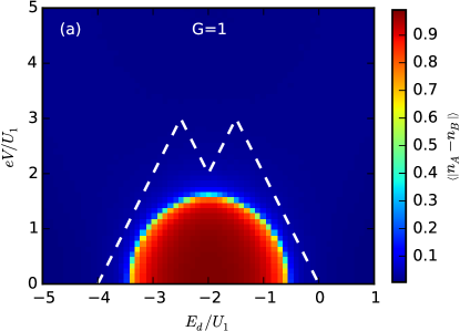

Figure 14 shows results for the checkerboard order parameter for a temperature of approximately two thirds of the Ising critical temperature and two values of , the particle-hole symmetric case and the large degeneracy . The observed shrinking of the regime with checkerboard order compared to is of course expected since higher temperatures allow additional tunneling processes that tend to destabilize charge order. For , the ordered regime is also shifted to larger , in accordance with the effective on-site energy (see Sec. III.3). Interestingly, for this large value of , the checkerboard conducting phase is found to be rather robust against thermal fluctuations.
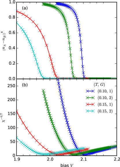
The character of the phase transitions can obviously not be inferred from Fig. 14. We exemplarily consider the transition between checkerboard and uniform phases driven by the bias voltage at a fixed on-site energy and several values of and . As in Sec. III.3, we plot the checkerboard order parameter to the power and the corresponding susceptibility to the power in Fig. 15. The results are consistent with the 2D Ising universality class Mitra et al. (2006); Pathria and Beale (2011); Sieberer et al. (2013); *PhysRevB.89.134310.
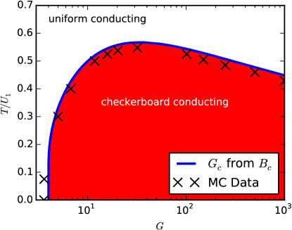
We finally turn to the checkerboard conducting regions, specifically the region , at nonzero temperatures. We found in Sec. III.3 that at there is a transition between uniform and checkerboard-ordered conducting states as the degeneracy is increased. For this, it is important that a checkerboard state cannot be destroyed by electrons tunneling in to create occupied defects in the empty sublattice since the corresponding rate vanishes. This is no longer true for ; for low temperatures there is now an exponentially small rate for creating such occupied defects. However, this in-tunneling rate contains a factor of so that for increasing the checkerboard state should eventually be destabilized in favor of a uniform state with occupancy close to unity. The same conclusion is reached by considering the effective on-site energy in the equivalent Ising model. This expectation is indeed borne out by the results presented in Fig. 16. We find a reentrant transition to the uniform conducting state at large , which shifts to smaller for increasing temperature. On the other hand, the transition to checkerboard order at lower shifts upwards with temperature. Both trends are consistent with the expectation that higher temperatures disfavor ordering. Above the corresponding critical temperature of the 2D Ising model, checkerboard order does not exist for any . Since Fig. 16 shows results for , i.e., in equilibrium, the critical temperature versus should map to the critical temperature versus applied magnetic field for the Ising model. Our simulation results indeed agree well with the conjecture of Müller-Hartmann and Zittartz Müller-Hartmann and Zittartz (1977).
V Summary and conclusions
In summary, we have studied a square lattice of quantum dots or molecules under a bias voltage applied perpendicular to the layer. We have assumed infinite on-site repulsion and finite nearest-neighbor Coulomb interaction within the layer, as well as vanishing intralayer hopping and weak monolayer-electrode hopping. The indirect hopping from a site in the monolayer to one of the electrodes and further to a different site of the monolayer is assumed to be fully incoherent, which is the case in the limits of short Fermi wavelength or strong disorder in the electrodes. By employing Monte Carlo simulations, we avoid mean-field approximations. The interactions lead to the appearance of charge-density-wave phases. Apart from the charge order, the main quantity of interest is the current perpendicular to the layer.
The resulting zero-temperature phase diagram, Fig. 10, shows blocked phases with vanishing current and zero, single, or checkerboard-ordered occupancy. The latter can be understood as a Coulomb-blockade state induced by the nearest-neighbor repulsion. These phases are connected to an equilibrium Ising model at . At larger bias voltages, they give way to conducting phases. Interestingly, it is possible for these phases to possess checkerboard charge order. This requires a high degeneracy of the occupied single-site states, which could be realized by combining charge and orbital degeneracies. The transition between the uniform conducting phase and the checkerboard conducting phase as a function of is in the 2D Ising universality class. The checkerboard conducting phase only exists out of equilibrium. In a large parameter range we find a transition from a uniform blocked phase to a checkerboard conducting phase at a finite critical bias voltage. This constitutes an interesting case of bias- or current-induced charge order. Furthermore, there is a region at finite bias voltage for which the two symmetry-related blocked checkerboard states are absorbing but the stationary state is nevertheless conducting and uniform. The presence of this active phase is evident in the current-voltage characteristics. It is interesting that such an active phase could be realized in a monolayer under bias, as there are not many experimental realizations. By judiciously taking the limit , we determine the phase transition between the absorbing and active phases to be in the 2D DP2 universality class.
The features found at are robust for small nonzero temperatures, except that absorbing states no longer exist for and that, as a consequence, the absorbing-to-active phase transition transforms into a 2D Ising transition between checkerboard blocked and uniform conducting phases. Apart from this change, the ordered phases shrink and, for degeneracies , shift to higher on-site energies for increasing temperature.
It would be desirable to extend the underlying dynamics to contain coherences as well as higher-order tunneling processes such as cotunneling and pair tunneling. Even in the absence of intralayer hopping, tunneling via the electrodes can induce coherences between eigenstates of the local particle numbers, i.e., delocalized charges in the monolayer. Intralayer hopping of course also favors delocalization in the monolayer. Higher-order processes and coherences are required for a study of Kondo-type effects in tunneling through the layer. Coherent hopping, be it direct or indirect through the electrodes, would turn the system into a much more difficult extended Hubbard model out of equilibrium. This would call for non-equilibrium quantum Monte Carlo simulations, which would suffer from the sign problem. On the other hand, a higher-order MFME including coherences seems feasible. In any case, even the quasi-classical model considered here should be valuable for further studies. On the one hand, comparison with experiments, for example on rolled-up structures, calls for a realistic description of electronic, spin, and vibrational degrees of freedom of molecular layers. On the other, further studies of the considered model might help to constrain the critical behavior of the 2D DP2 universality class.
Acknowledgements.
We would like to thank S. Diehl, J. Marino, A. Rubio, T. Vojta, and A. Wacker for useful discussions. Financial support by the Deutsche Forschungsgemeinschaft, through Research Unit FOR 1154, Towards Molecular Spintronics, is gratefully acknowledged. C. T. also acknowledges support by the Deutsche Forschungsgemeinschaft through Collaborative Research Center SFB 1143.References
- Itskevich et al. (1996) I. E. Itskevich, T. Ihn, A. Thornton, M. Henini, T. J. Foster, P. Moriarty, A. Nogaret, P. H. Beton, L. Eaves, and P. C. Main, Phys. Rev. B 54, 16401 (1996).
- Narihiro et al. (1997) M. Narihiro, G. Yusa, Y. Nakamura, T. Noda, and H. Sakaki, Appl. Phys. Lett. 70, 105 (1997).
- Suzuki et al. (1997) T. Suzuki, K. Nomoto, K. Taira, and I. Hase, Japanese J. Appl. Phys. 36, 1917 (1997).
- Hapke-Wurst et al. (1999) I. Hapke-Wurst, U. Zeitler, H. W. Schumacher, R. J. Haug, K. Pierz, and F. J. Ahlers, Semicond. Sci. Technol. 14, L41 (1999).
- Belyaev et al. (2001) A. Belyaev, L. Eaves, S. Vitusevich, P. Main, M. Henini, A. Förster, N. Klein, and S. Danylyuk, in Proceedings of the 25th International Conference on the Physics of Semiconductors (ICPS 25), edited by N. Miura (Springer, 2001).
- Hapke-Wurst et al. (2003) I. Hapke-Wurst, U. Zeitler, U. F. Keyser, R. J. Haug, K. Pierz, and Z. Ma, Appl. Phys. Lett. 82, 1209 (2003).
- Lin and Lee (2003) S. D. Lin and C. P. Lee, J. Appl. Phys. 93, 2952 (2003).
- Pulizzi et al. (2003) F. Pulizzi, E. E. Vdovin, K. Takehana, Y. V. Dubrovskii, A. Patanè, L. Eaves, M. Henini, P. N. Brunkov, and G. Hill, Phys. Rev. B 68, 155315 (2003).
- Austing et al. (2005) D. Austing, R. Hill, A. Patanè, P. Main, M. Henini, L. Eaves, and S. Tarucha, Physica E 26, 482 (2005).
- Sun et al. (2006) J. Sun, P. Jin, C. Zhao, L. Yu, X. Ye, B. Xu, Y. Chen, and Z. Wang, J. Electrochem. Soc. 153, G703 (2006).
- Vdovin et al. (2007) E. E. Vdovin, Y. N. Khanin, O. Makarovsky, Y. V. Dubrovskii, A. Patanè, L. Eaves, M. Henini, C. J. Mellor, K. A. Benedict, and R. Airey, Phys. Rev. B 75, 115315 (2007).
- Swart et al. (2016) I. Swart, P. Liljeroth, and D. Vanmaekelbergh, Chemical Reviews (2016), 10.1021/acs.chemrev.5b00678, pMID: 26900754.
- Bigelow et al. (1946) W. C. Bigelow, D. L. Pickett, and W. A. Zisman, J. Coll. Sci. 1, 513 (1946).
- Scheffler et al. (2013) M. Scheffler, L. Smykalla, D. Baumann, R. Schlegel, T. Hänke, M. Toader, B. Büchner, M. Hietschold, and C. Hess, Surf. Sci. 608, 55 (2013).
- Smykalla et al. (2015) L. Smykalla, P. Shukrynau, M. Korb, H. Lang, and M. Hietschold, Nanoscale 7, 4234 (2015).
- Poirier et al. (1994) G. E. Poirier, M. J. Tarlov, and H. E. Rushmeier, Langmuir 10, 3383 (1994).
- Vuillaume et al. (1996) D. Vuillaume, C. Boulas, J. Collet, J. V. Davidovits, and F. Rondelez, Appl. Phys. Lett. 69, 1646 (1996).
- Whitesides and Boncheva (2002) G. M. Whitesides and M. Boncheva, Proc. Natl. Acad. Sci. U.S.A. 99, 4769 (2002).
- Lodha and Janes (2004) S. Lodha and D. B. Janes, Appl. Phys. Lett. 85, 2809 (2004).
- Prinz et al. (2000) V. Prinz, V. Seleznev, A. Gutakovsky, A. Chehovskiy, V. Preobrazhenskii, M. Putyato, and T. Gavrilova, Physica E 6, 828 (2000).
- Schmidt and Eberl (2001) O. G. Schmidt and K. Eberl, Nature 410, 168 (2001).
- Bof Bufon et al. (2014) C. C. Bof Bufon, C. Vervacke, D. J. Thurmer, M. Fronk, G. Salvan, S. Lindner, M. Knupfer, D. R. T. Zahn, and O. G. Schmidt, The J. Phys. Chem. C 118, 7272 (2014).
- Bof Bufon et al. (2010) C. C. Bof Bufon, J. D. Cojal González, D. J. Thurmer, D. Grimm, M. Bauer, and O. G. Schmidt, Nano Lett. 10, 2506 (2010).
- Thurmer et al. (2010) D. J. Thurmer, C. C. Bof Bufon, C. Deneke, and O. G. Schmidt, Nano Lett. 10, 3704 (2010).
- Bof Bufon et al. (2011) C. C. Bof Bufon, J. D. Arias Espinoza, D. J. Thurmer, M. Bauer, C. Deneke, U. Zschieschang, H. Klauk, and O. G. Schmidt, Nano Lett. 11, 3727 (2011).
- Müller et al. (2012) C. Müller, C. C. Bof Bufon, M. E. Navarro Fuentes, D. Makarov, D. H. Mosca, and O. G. Schmidt, Appl. Phys. Lett. 100, 022409 (2012).
- Grimm et al. (2013) D. Grimm, C. C. Bof Bufon, C. Deneke, P. Atkinson, D. J. Thurmer, F. Schäffel, S. Gorantla, A. Bachmatiuk, and O. G. Schmidt, Nano Lett. 13, 213 (2013).
- Vilan et al. (2000) A. Vilan, A. Shanzer, and D. Cahen, Nature 404, 166 (2000).
- Vilan and Cahen (2002) A. Vilan and D. Cahen, Adv. Funct. Mater. 12, 795 (2002).
- Stein et al. (2010) N. Stein, R. Korobko, O. Yaffe, R. H. Lavan, H. Shpaisman, E. Tirosh, A. Vilan, and D. Cahen, The J. Phys. Chem. C 114, 12769 (2010).
- Tian et al. (2003) M. Tian, J. Wang, J. Kurtz, T. E. Mallouk, and M. H. W. Chan, Nano Lett. 3, 919 (2003).
- Coll et al. (2009) M. Coll, L. H. Miller, L. J. Richter, D. R. Hines, O. D. Jurchescu, N. Gergel-Hackett, C. A. Richter, and C. A. Hacker, J. Am. Chem. Soc. 131, 12451 (2009).
- Wang et al. (2011) G. Wang, Y. Kim, M. Choe, T.-W. Kim, and T. Lee, Adv. Mater. 23, 755 (2011).
- Vuillaume (2010) D. Vuillaume, in Oxford Handbook of Nanoscience and Technology, Vol. 3, edited by A. Narlikar and Y. Fu (Oxford University Press, 2010) Chap. 9, pp. 312–342.
- Andergassen et al. (2010) S. Andergassen, V. Meden, H. Schoeller, J. Splettstoesser, and M. R. Wegewijs, Nanotechnology 21, A262001 (2010).
- Bruus and Flensberg (2004) H. Bruus and K. Flensberg, Many-Body Quantum Theory in Condensed Matter Physics (Oxford University Press, 2004).
- Hohenberg and Halperin (1977) P. C. Hohenberg and B. I. Halperin, Rev. Mod. Phys. 49, 435 (1977).
- Cross and Hohenberg (1993) M. C. Cross and P. C. Hohenberg, Rev. Mod. Phys. 65, 851 (1993).
- Hinrichsen (2000) H. Hinrichsen, Adv. Phys. 49, 815 (2000).
- Ódor (2004) G. Ódor, Rev. Mod. Phys. 76, 663 (2004).
- Kießlich et al. (2002) G. Kießlich, A. Wacker, and E. Schöll, Physica B 314, 459 (2002).
- Kießlich et al. (2003) G. Kießlich, A. Wacker, E. Schöll, S. A. Vitusevich, A. E. Belyaev, S. V. Danylyuk, A. Förster, N. Klein, and M. Henini, Phys. Rev. B 68, 125331 (2003).
- Wetzler et al. (2003) R. Wetzler, A. Wacker, and E. Schöll, Phys. Rev. B 68, 045323 (2003).
- Wetzler et al. (2004) R. Wetzler, R. Kunert, A. Wacker, and E. Schöll, New J. Phys. 6, 81 (2004).
- Leijnse (2013) M. Leijnse, Phys. Rev. B 87, 125417 (2013).
- Mitra et al. (2006) A. Mitra, S. Takei, Y. B. Kim, and A. J. Millis, Phys. Rev. Lett. 97, 236808 (2006).
- Bolvin and Kahn (1995a) H. Bolvin and O. Kahn, Chem. Phys. 192, 295 (1995a).
- Bolvin and Kahn (1995b) H. Bolvin and O. Kahn, Chem. Phys. Lett. 243, 355 (1995b).
- A. Bousseksou et al. (1995) A. Bousseksou, H. Constant-Machado, and F. Varret, J. Phys. I France 5, 747 (1995).
- Yokoyama et al. (1998) T. Yokoyama, Y. Murakami, M. Kiguchi, T. Komatsu, and N. Kojima, Phys. Rev. B 58, 14238 (1998).
- Breuer and Petruccione (2007) H.-P. Breuer and F. Petruccione, The Theory of Open Quantum Systems (Oxford University Press, 2007).
- Timm (2008) C. Timm, Phys. Rev. B 77, 195416 (2008).
- Wangsness and Bloch (1953) R. K. Wangsness and F. Bloch, Phys. Rev. 89, 728 (1953).
- Bloch (1957) F. Bloch, Phys. Rev. 105, 1206 (1957).
- Redfield (1965) A. G. Redfield, Adv. Magn. Reson. 1, 1 (1965).
- Wick et al. (1952) G. C. Wick, A. S. Wightman, and E. P. Wigner, Phys. Rev. 88, 101 (1952).
- Wick et al. (1970) G. C. Wick, A. S. Wightman, and E. P. Wigner, Phys. Rev. D 1, 3267 (1970).
- Zurek (1982) W. H. Zurek, Phys. Rev. D 26, 1862 (1982).
- Giulini et al. (1995) D. Giulini, C. Kiefer, and H. Zeh, Phys. Lett. A 199, 291 (1995).
- Elste and Timm (2005) F. Elste and C. Timm, Phys. Rev. B 71, 155403 (2005).
- Timm (2011) C. Timm, Phys. Rev. B 83, 115416 (2011).
- Note (1) Kinetic simulations would require us to advance the simulation time by an exponentially distributed time with this mean. However, for the long-time limit we are interested in, both prescriptions give the same results.
- Bortz et al. (1975) A. Bortz, M. Kalos, and J. Lebowitz, J. Comput. Phys. 17, 10 (1975).
- Gillespie (1976) D. T. Gillespie, J. Comput. Phys. 22, 403 (1976).
- Gillespie (1977) D. T. Gillespie, J. Phys. Chem. 81, 2340 (1977).
- Schulze (2002) T. P. Schulze, Phys. Rev. E 65, 036704 (2002).
- Swendsen and Wang (1986) R. H. Swendsen and J.-S. Wang, Phys. Rev. Lett. 57, 2607 (1986).
- Wolff (1989) U. Wolff, Phys. Rev. Lett. 62, 361 (1989).
- Pathria and Beale (2011) R. K. Pathria and P. D. Beale, Statistical mechanics, 3rd ed. (Elsevier/Academic Press, 2011).
- Müller-Hartmann and Zittartz (1977) E. Müller-Hartmann and J. Zittartz, Z. Phys. B: Condens. Matter 27, 261 (1977).
- Mahan and Claro (1977) G. D. Mahan and F. H. Claro, Phys. Rev. B 16, 1168 (1977).
- Note (2) One might ask whether the rate equations really describe relaxation into these ground states. This is the case if we set and then take the limit since the system is ergodic for any .
- Blöte and den Nijs (1988) H. W. J. Blöte and M. P. M. den Nijs, Phys. Rev. B 37, 1766 (1988).
- Sieberer et al. (2013) L. M. Sieberer, S. D. Huber, E. Altman, and S. Diehl, Phys. Rev. Lett. 110, 195301 (2013).
- Sieberer et al. (2014) L. M. Sieberer, S. D. Huber, E. Altman, and S. Diehl, Phys. Rev. B 89, 134310 (2014).
- Note (3) Raising also increases the rate for creating an occupied defect on the empty sublattice, which destabilizes the order, but for this to happen more than one empty defect at neighboring sites is needed, which makes the overall creation rate of such defects much smaller than the overall rate for removing empty defects.
- Ferrell et al. (1967) R. A. Ferrell, N. Menyhárd, H. Schmidt, F. Schwabl, and P. Szépfalusy, Phys. Rev. Lett. 18, 891 (1967).
- Ferrell et al. (1968) R. Ferrell, N. Menyhàrd, H. Schmidt, F. Schwabl, and P. Szépfalusy, Ann. Phys. 47, 565 (1968).
- Halperin and Hohenberg (1969) B. I. Halperin and P. C. Hohenberg, Phys. Rev. 177, 952 (1969).
- Grassberger and de la Torre (1979) P. Grassberger and A. de la Torre, Ann. Phys. 122, 373 (1979).
- Muñoz et al. (1997) M. A. Muñoz, G. Grinstein, and Y. Tu, Phys. Rev. E 56, 5101 (1997).
- Lee and Vojta (2011) M. Y. Lee and T. Vojta, Phys. Rev. E 83, 011114 (2011).
- Hinrichsen (1997) H. Hinrichsen, Phys. Rev. E 55, 219 (1997).
- Dornic et al. (2001) I. Dornic, H. Chaté, J. Chave, and H. Hinrichsen, Phys. Rev. Lett. 87, 045701 (2001).
- Venkataraman et al. (2007) L. Venkataraman, Y. S. Park, A. C. Whalley, C. Nuckolls, M. S. Hybertsen, and M. L. Steigerwald, Nano Letters 7, 502 (2007).
- Mowbray et al. (2008) D. J. Mowbray, G. Jones, and K. S. Thygesen, The Journal of Chemical Physics 128, 111103 (2008).