Ultra-broadband nanophotonic beamsplitter using an anisotropic sub-wavelength metamaterial
Nanophotonic beamsplitters are fundamental building blocks in integrated optics, with applications ranging from high speed telecom receivers to biological sensors and quantum splitters. While high-performance multiport beamsplitters have been demonstrated in several material platforms using multimode interference couplers, their operation bandwidth remains fundamentally limited. Wavelength independent integrated beamsplitters would enable breakthrough broadband integrated photonic systems for communications, sensing and quantum physics. Here, we leverage for the first time the inherent anisotropy and dispersion of a sub-wavelength structured photonic metamaterial to demonstrate ultra-broadband integrated beamsplitting. Our device, which is three times more compact than its conventional counterpart, can achieve virtually perfect operation over an unprecedented design bandwidth exceeding all optical communication bands combined, and making it the most broadband silicon photonics component reported to date. Our demonstration paves the way toward nanophotonic waveguide components with ultra-broadband operation for next generation integrated photonic systems.
Integrated photonic systems are poised to produce key advances in areas such as optical communications [1, 2], sensing [3, 4], spectroscopy [5, 6], metrology [7], frequency comb generation [8] and quantum physics [9, 10]. Since beamsplitters are fundamental photonic building blocks, substantially extending their operational bandwidth would pave the way towards broadband systems capable, for instance, of covering several optical communication bands, or realizing sensors and frequency combs over large spectral regions as required in optical coherence tomography. Integrated beamsplitters are preferably implemented with multimode interference couplers (MMIs), which exploit the self-imaging effect discovered by Henry Talbot in the 1830s [11]. Talbot imaging allows to form multiport couplers with well defined amplitude and phase ratios that offer improved performance compared to y-branches and directional couplers [12, 13]. MMI couplers are used in a wide variety of waveguide devices [1, 10, 14, 15, 16, 17, 18], and have been implemented in a broad range of material platforms [19, 20, 21, 22]. However, until very recently, the same classical structure, similar to the one shown in Fig. 1 for a MMI configuration, has been used. Consisting of an essentially rectangular central multimode region with tapered input and output waveguides, it provides a rugged design, but also imposes fundamental restrictions in terms of size and bandwidth [23, 13]. On the other hand, the recent advent of sub-wavelength grating (SWG) metamaterial waveguides, which suppress diffraction effects, has enabled the concept of refractive index engineering [24, 25]. This concept has ushered in breakthrough devices for fiber-to-chip coupling [26, 27], wavelength multiplexing [28], and polarization splitting [29], among other innovations. Applied to MMIs, sub-wavelength index engineering led to the first demonstration of a slotted MMI [30], which reduced the size of the device by a factor of two compared to a conventional MMI, without affecting its performance.
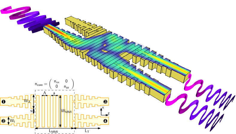
Here we examine, for the first time, self-imaging in an anisotropic sub-wavelength structure and exploit this new concept, in combination with dispersion engineering [31], to experimentally demonstrate a compact and ultra-broadband MMI (see Fig. 2). Our fabricated device yields a threefold size reduction compared to a conventional device, while at the same time achieving perfect performance (excess losses and imbalance , phase error ) over an unprecedented bandwidth of more than around a central wavelength of , limited by our measurement setup. Full 3D simulations predict the bandwidth exceeding ; in simulation an optimized conventional MMI design covers less than with comparable performance. To the best of our knowledge this not only constitutes the MMI with the broadest bandwidth ever demonstrated, but also one of the most broadband, fully passive integrated optical devices in general.
Results
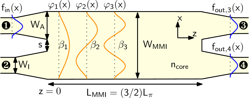
Self-imaging revisted. We first focus on the 2D model of the MMI shown in Fig. 1 and 2 in order to compare self-imaging in conventional and sub-wavelength engineered MMIs. In this 2D model the -axis is contracted using the effective index method [32]. In both devices the mode field launched from the input waveguide, , is expanded into the modes of the multimode slab region, i.e. , with the overlap between the input field and the -th slab mode. These modes propagate with specific phase constants, , producing self-images of the input field as they interfere. The positions at which these images form is governed by the beat length of the two lowest order modes [13],
| (1) |
For instance, a double image of the input field is formed at , where is the physical length of the multimode region (see Fig. 1). Since is fixed, any wavelength variation of the beat length will result in a detuning of the device and in a significant degradation of its performance.
Conventional multimode interference. In a conventional MMI, under the paraxial approximation, the beat length is given by
| (2) |
where is the effective index of the multimode region obtained with the effective index method [32] and is the free space wavelength. is the effective width of the multimode region taking into account the Goos-Hänchen shift, which is assumed to be identical for all modes and invariant with wavelength [13]. The choice of the material platform clearly dictates the value of and its wavelength dependence. The minimum width of the multimode region is determined by the separation () between the input/output waveguides, to avoid coupling between them, and the required width of the access waveguides (), to control the excitation of higher order modes; see [33, 15] for details. Hence, there is very limited freedom to engineer the beat length or its wavelength dependence.
| Parameter | Conventional | Broadband |
|---|---|---|
| Silicon thickness () | ||
| Width MMI () | ||
| Length MMI () | ||
| Width input () | ||
| Width access () | ||
| Length taper () | ||
| Separation () | ||
| Period () | – | |
| Duty cycle (DC) | – | 50 % |
| @ | ||
Considering a thick silicon platform with silicon dioxide () upper cladding, TE polarization, and the geometrical parameters given in table 1, Eq. (2) yields at . Figure 3(a) shows the beat length calculated through Eq. (1), with obtained from a slab waveguide of width , silicon dioxide cladding, and effective core index . The beat length is at , in good agreement with Eq. (2). However, due to the strong wavelength dependence, the device will only operate in a limited bandwidth of as discussed below.
Multimode interference in anisotropic media. The fundamental advantage of our broadband MMI device, shown in Fig. 2, arises from the inherent anisotropy of its sub-wavelength structure: two guided waves traveling in the central multimode region along the and directions experience optically different structures [34, 35]. Referring to the effective indexes of these waves as and , respectively, we see that in the 2D model shown in Fig. 1 the equivalent material in the multimode region can be described by the diagonal tensor . In such an anisotropic medium, the dispersion equation is given by , where is the wave-vector component in the direction, is the propagation constant, and [36]. Extending the procedure outlined in [13] for conventional isotropic MMIs, we find that in the anisotropic case the beat length is given by:
| (3) |
Equation (3) provides an analytical design framework for our ultra-broadband MMIs.
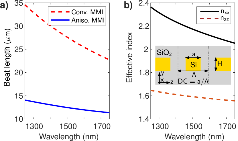
The elements of effective index tensor can be calculated from the structure shown in the inset of Fig. 3(b): is the effective index of the fundamental Bloch mode traveling in the direction and polarized along the axis; is the effective index of the fundamental Bloch mode traveling in the direction and polarized along the axis. For the dimensions given in table 1, we obtain the indexes shown in Fig. 3(b); specifically at we have , . Equation (3) then predicts a significantly reduced beat length of , which arises directly from the reduced value of compared to [see Eqs. (2) and (3)]. Since the variation of and with wavelength is, to first order, proportional to and , the wavelength dependence of the beat length is expected to decrease, too. Figure 3(a) shows the beat length calculated through Eq. (1), with obtained from an anisotropic slab waveguide of width , silicon dioxide cladding, and [36]. From the figure, we find at , in good agreement with Eq. (3), and observe that the beat length becomes significantly flatter with wavelength. We furthermore found that the beat length is minimum for a duty cycle of , which facilitates fabrication, as it results in the largest linewidths for a given grating period. It is noted that the precise dispersion behavior of the MMI modes near their Bragg wavelength can only be obtained in full 3D simulations, which enables us to further flatten the beat length by fine-tuning the pitch of the structure.
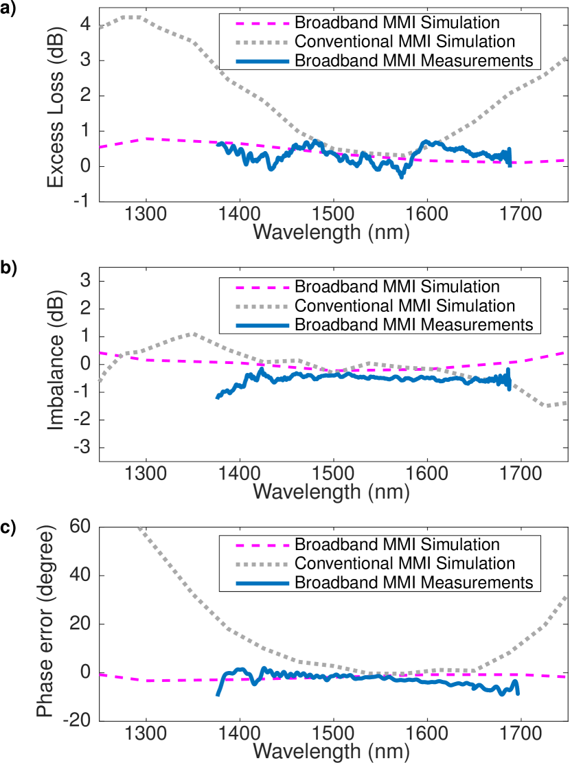
Design and simulation. We use full 3D simulations to assess and further optimize the performance of both the conventional and the sub-wavelength metamaterial engineered MMI. Figure 4 shows the simulated wavelength dependence of the beat length of a conventional MMI; the propagation constants were obtained with a commercial mode solver [37]. As expected from the 2D model [Fig. 3(a)], the beat length exhibits a strong variation with wavelength, between and , resulting in performance degratation when de-tuning the device from its design wavelenght. For a conventional MMI with the optimized dimensions shown in table 1, the simulated impact of this de-tuning is shown Fig. 5, including the excess losses (EL), imbalance (IB) and phase error (PE). By denoting the complex transmission from the fundamental mode of input waveguide 1 to the fundamental mode of the output waveguides 3 and 4 as and (see Fig. 1), these performance parameters are: , , and . From Figs. 5(a)-(c) it is obvious that as the device is operated further away from its design wavelength its performance steadily deteriorates. Aiming for excess losses and imbalance below and phase error smaller than thus yields a bandwidth of under for this optimized MMI design.
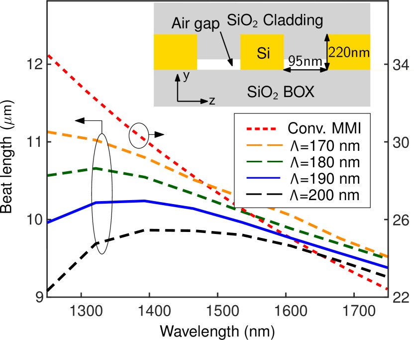
The wavelength dependence of the beat length in our sub-wavelength engineered MMI (see Fig. 2) is shown, for a duty cycle, in Fig. 4; the propagation constants were obtained using 3D Finite Difference Time Domain (FDTD) simulations [38], and the procedure described in [39]. For the device parameters given in table 1, we find that by fine-tuning the pitch near , and thereby adjusting the dispersion of the MMI modes, the beat length becomes virtually wavelength independent in the to wavelength range. Furthermore, the beat length at is , which is a threefold reduction compared to the conventional device. The inset of Fig. 4 illustrates the longitudinal cross-section of the MMI. In our initial design we assumed that the upper would completely fill the trenches between the silicon segments. However, our experimental results suggest that this is not the case, and that in fact an air gap of approximately is left, due to the relatively high aspect ratio of the trenches. All 3D simulation results presented here include this gap.
For a pitch of the wavelength average beat length is , yielding a device with approximately for a MMI device. We optimized the length of the device using 3D-FDTD simulations of the complete structure that take into account material dispersion. Device performance for the optimized length of is shown in Fig. 5. These results confirm virtually perfect device operation over a wavelength span, with excess losses and imbalance below , and phase error less than . This is an unprecedented almost threefold bandwidth enhancement compared to the conventional MMI.
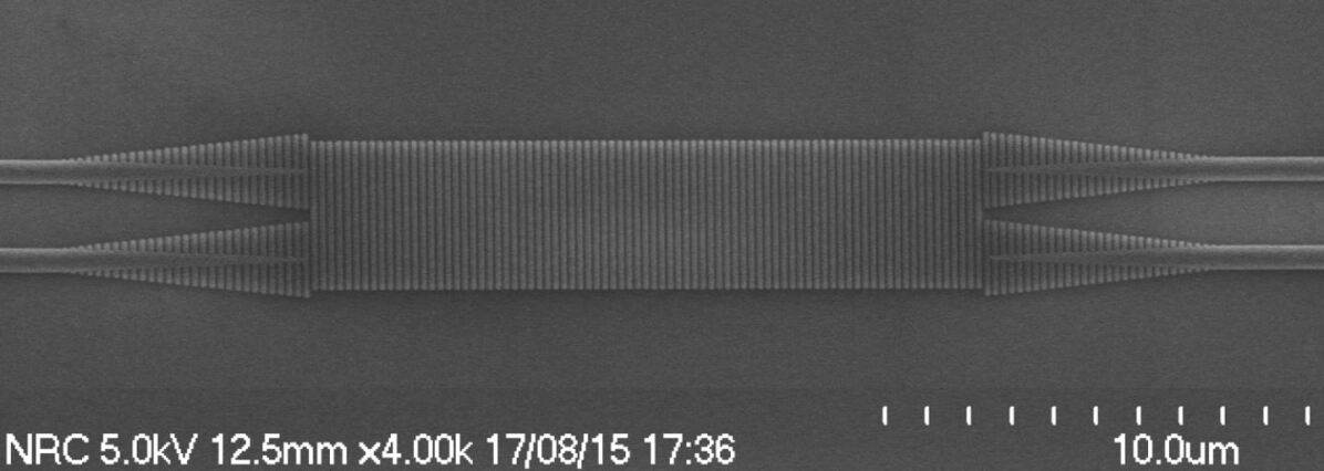
Experimental results. In order to experimentally validate the broadband operation of our device, several test structures were fabricated on a standard silicon-on-insulator wafer, as described in the methods. Figure 6 shows a Scanning Electron Microscope (SEM) image of one of the fabricated devices prior to the deposition of the upper cladding. Measurements of the devices were carried out on two independent setups (see methods). The experimental results shown in Fig. 5 reveal virtually perfect device performance in the - wavelength range: excess losses and imbalance are below , and the phase error is smaller than , thereby confirming the broadband behavior of the device. We observed a resonant behavior near , which is attributed to the increased duty cycle of the fabricated devices and could be addressed with proper pre-scaling of the mask. Our broadband source does not extend beyond preventing measurements at longer wavelengths.
Discussion
In conclusion, we have shown that the intrinsic anisotropy of sub-wavelength engineered metamaterials can be exploited to design compact and ultra-broadband nanophotonic beam splitters. Specifically, by controlling anisotropy and dispersion of a nanophotonic metamaterial waveguide, we have demonstrated MMI designs with virtually ideal performance over a and have fabricated a device with a measured bandwidth in excess of , outperforming conventional MMIs by a wide margin. We believe that this new strategy to engineer ultra-broadband waveguide devices can usher in broadband integrated nanophotonic systems with applications in coherent communications, sensing, spectroscopy and quantum photonics.
Methods
Fabrication. We fabricated a chip containing both individual MMIs, asymmetric Mach-Zehnder interferometers and reference waveguides. To enable broadband light coupling to the chip we used sub-wavelength engineered fiber-to-chip mode transformers [26]. The devices were defined with electron beam lithography and transferred to the silicon layer with reactive ion etching. The upper cladding was deposited using plasma-enhanced chemical vapor deposition.
Measurements. The devices were characterized with two independent setups. An initial screening of the devices was carried out using a tunable laser source at the input and power-detector at the output, covering the to range. In order to measure in an even broader range, we used a second setup with a broadband light source as input and an optical spectrum analyzer at the output. In both cases the input polarization was set to quasi-TE (electric field in the horizontal plane) using a polarization controller. To determine excess losses, the transmission through an individual MMI was normalized to the transmission through a reference waveguide. The phase error was obtained from the interferogram produced by the asymmetric Mach-Zehnder interferometers, using a minimum-phase technique [40]. The measurement data from both setups was found to be in very good agreement in the common wavelength range, with a deviation below in phase, in imbalance and in excess loss.
References
- [1] Dong, P. et al. Monolithic silicon photonic integrated circuits for compact 100 Gb/s coherent optical receivers and transmitters. IEEE J. Sel. Top. Quantum Electron. 20, 150–157 (2014).
- [2] Sano, A. et al. 102.3-Tb/s (224 548-Gb/s) C-and extended L-band all-Raman transmission over 240 km using PDM-64QAM single carrier FDM with digital pilot tone. In National Fiber Optic Engineers Conference, PDP5C–3 (Optical Society of America, 2012).
- [3] Estevez, M.-C., Alvarez, M. & Lechuga, L. M. Integrated optical devices for lab-on-a-chip biosensing applications. Laser Photonics Rev. 6, 463–487 (2012).
- [4] Rodrigo, D. et al. Mid-infrared plasmonic biosensing with graphene. Science 349, 165–168 (2015).
- [5] Nedeljkovic, M. et al. Mid-infrared silicon-on-insulator fourier-transform spectrometer chip. IEEE Photonic Tech. L. 28, 528–531 (2016).
- [6] Le Coarer, E. et al. Wavelength-scale stationary-wave integrated fourier-transform spectrometry. Nat. Photonics 1, 473–478 (2007).
- [7] Pasquazi, A. et al. Sub-picosecond phase-sensitive optical pulse characterization on a chip. Nat. Photonics 5, 618–623 (2011).
- [8] Razzari, L. et al. CMOS-compatible integrated optical hyper-parametric oscillator. Nat. Photonics 4, 41–45 (2010).
- [9] Crespi, A. et al. Anderson localization of entangled photons in an integrated quantum walk. Nat. Photonics 7, 322–328 (2013).
- [10] He, J. et al. Ultracompact quantum splitter of degenerate photon pairs. Optica 2, 779–782 (2015).
- [11] Talbot, H. F. Facts relating to optical science. Philos. Mag. 9, 401–407 (1836).
- [12] Ulrich, R. & Ankele, G. Self-imaging in homogeneous planar optical waveguides. Appl. Phys. Lett. 27, 337–339 (1975).
- [13] Soldano, L. B. & Pennings, E. Optical multi-mode interference devices based on self-imaging: principles and applications. J. Lightwave Technol. 13, 615–627 (1995).
- [14] Runge, P. et al. Monolithic InP receiver chip with a 90∘ hybrid and 56 GHz balanced photodiodes. Opt. Express 20, B250–B255 (2012).
- [15] Halir, R., Roelkens, G., Ortega-Moñux, A. & Wangüemert-Pérez, J. G. High-performance 90∘ hybrid based on a silicon-on-insulator multimode interference coupler. Opt. Lett. 36, 178–180 (2011).
- [16] Zhang, Y., Hosseini, A., Xu, X., Kwong, D. & Chen, R. T. Ultralow-loss silicon waveguide crossing using Bloch modes in index-engineered cascaded multimode-interference couplers. Opt. Lett. 38, 3608–3611 (2013).
- [17] Kleijn, E., Smit, M. & Leijtens, X. Multimode interference reflectors: A new class of components for photonic integrated circuits. J. Lightwave Technol. 31, 3055–3063 (2013).
- [18] Fandiño, J. S., Doménech, J. D. & Muñoz, P. Two-port multimode interference reflectors based on aluminium mirrors in a thick SOI platform. Opt. Express 23, 20219–20233 (2015).
- [19] Tajaldini, M. & Jafri, M. Simulation of an ultra-compact multimode interference power splitter based on kerr nonlinear effect. J. Lightwave Technol. 32, 1282–1289 (2014).
- [20] Zhu, Z., Garcia-Ortiz, C. E., Han, Z., Radko, I. P. & Bozhevolnyi, S. I. Compact and broadband directional coupling and demultiplexing in dielectric-loaded surface plasmon polariton waveguides based on the multimode interference effect. Appl. Phys. Lett. 103, 061108 (2013).
- [21] Guan, X., Wu, H., Shi, Y. & Dai, D. Extremely small polarization beam splitter based on a multimode interference coupler with a silicon hybrid plasmonic waveguide. Opt. Lett. 39, 259–262 (2014).
- [22] Zheng, R., Gao, D. & Dong, J. Ultra-compact broadband tunable graphene plasmonic multimode interferometer. IEEE Photonic Tech. L. 28, 645 – 648 (2016).
- [23] Besse, P. A., Bachmann, M., Melchior, H., Soldano, L. B. & Smit, M. K. Optical bandwidth and fabrication tolerances of multimode interference couplers. J. Lightwave Technol. 12, 1004–1009 (1994).
- [24] Cheben, P. et al. Refractive index engineering with subwavelength gratings for efficient microphotonic couplers and planar waveguide multiplexers. Opt. Lett. 35, 2526–2528 (2010).
- [25] Halir, R. et al. Waveguide sub-wavelength structures: a review of principles and applications. Laser Photonics Rev. 9, 25–49 (2015).
- [26] Cheben, P. et al. Broadband polarization independent nanophotonic coupler for silicon waveguides with ultra-high efficiency. Opt. Express 23, 22553–22563 (2015).
- [27] Benedikovic, D. et al. Subwavelength index engineered surface grating coupler with sub-decibel efficiency for 220-nm silicon-on-insulator waveguides. Opt. Express 23, 22628–22635 (2015).
- [28] Piggott, A. Y. et al. Inverse design and demonstration of a compact and broadband on-chip wavelength demultiplexer. Nat. Photonics 9, 374–377 (2015).
- [29] Shen, B., Wang, P., Polson, R. & Menon, R. An integrated-nanophotonics polarization beamsplitter with footprint. Nat. Photonics 9, 378–382 (2015).
- [30] Ortega-Moñux, A. et al. An ultra-compact multimode interference coupler with a subwavelength grating slot. Laser Photonics Rev. 7, L12–L15 (2013).
- [31] Maese-Novo, A. et al. Wavelength independent multimode interference coupler. Opt. Express 21, 7033–7040 (2013).
- [32] Chen, C.-L. Foundations for Guided-Wave Optics (Wiley, 2006).
- [33] Halir, R. et al. A design procedure for high-performance, rib-waveguide-based multimode interference couplers in silicon-on-insulator. J. Lightwave Technol. 26, 2928–2936 (2008).
- [34] Bouchitte, G. & Petit, R. Homogenization techniques as applied in the electromagnetic theory of gratings. Electromagnetics 5, 17–36 (1985).
- [35] Gu, C. & Yeh, P. Form birefringence dispersion in periodic layered media. Opt. Lett. 21, 504–506 (1996).
- [36] Satomura, Y., Matsuhara, M. & Kumagai, N. Analysis of electromagnetic-wave modes in anisotropic slab waveguide. IEEE T. Microw. Theory 22, 86–92 (1974).
- [37] Fimmwave & Fimmprop, available from Photon Design. https://www.photond.com.
- [38] Fullwave, available from RSoft. http://www.rsoftdesign.com.
- [39] Wangüemert-Pérez, J. G. et al. Evanescent field waveguide sensing with subwavelength grating structures in silicon-on-insulator. Opt. Lett. 39, 4442–4445 (2014).
- [40] Halir, R. et al. Characterization of integrated photonic devices with minimum phase technique. Opt. Express 17, 8349–8361 (2009).
Acknowledgements
We acknowledge funding from the Ministerio de Economía y Competitividad, Programa Estatal de Investigación, Desarrollo e Innovación Orientada a los Retos de la Sociedad (cofinanciado FEDER), Proyecto TEC2013-46917-C2-1-R. We would like to thank Dr. Jean Lapointe for preparing files for e-beam lithography.