,
Landau Levels in 2D materials using Wannier Hamiltonians obtained by first principles
Abstract
We present a method to calculate the Landau levels and the corresponding edge states of two dimensional (2D) crystals using as a starting point their electronic structure as obtained from standard density functional theory (DFT). The DFT Hamiltonian is represented in the basis of maximally localized Wannier functions. This defines a tight-binding Hamiltonian for the bulk that can be used to describe other structures, such as ribbons, provided that atomic scale details of the edges are ignored. The effect of the orbital magnetic field is described using the Peierls substitution in the hopping matrix elements. Implementing this approach in a ribbon geometry, we obtain both the Landau levels and the dispersive edge states for a series of 2D crystals, including graphene, Boron Nitride, MoS2, Black Phosphorous, Indium Selenide and MoO3. Our procedure can readily be used in any other 2D crystal, and provides an alternative to effective mass descriptions.
I Introduction
The motion of electrons in two dimensions under the influence of a perpendicular magnetic field results in a discrete spectrum of energy levels, associated to the bound closed cyclotron orbits expected within the classical picture. In the case of Schrodinger electrons, the discrete spectrum was first calculated by Landau,landau1962 that showed that , where are integer numbers and , where and are the charge and mass of the electron. The concept of Landau levels (LL) is also useful in systems for which the effective mass approximation is a good description of the relevant energy bands, such as semiconductor two dimensional electron gases.AndoRMP With the observation of the unconventional quantum Hall effect in graphene,novoselov2005 ; Zhang2005 it was soon realized that the spectrum of quantized levels was different from the usual Landau quantization, and they would rather scale as , with and being the Fermi velocity of graphene carriers. This unconventional spectrum of Landau Levels can easily be obtained using the effective mass Hamiltonian for graphene, isomorphic to the celebrated Dirac Hamiltonian.
The physics of the magnetic quantum oscillationsgillgren2014gate ; li2015quantum ; tayari2015two and, in the extreme quantum limit, the quantum Hall effect of a given system, are often best described in terms its Landau levels. The quest for samples with increased mobility has finally led to the observation of the quantum Hall effect in few layer Black Phosphorous,li2016 in thin film transition metal disulfides wu2015 and monolayer WSe2PhysRevLett.116.086601 which provides an experimental motivation for this work. Importantly, the properties of Landau levels can be dramatically different depending on the symmetry of the crystal. Thus, hexagonal crystals such as graphenezheng2002 and MoS2Niu2013 have Landau levels that can be accounted for in terms of two sets of Dirac electrons, one per valley, whereas in the case of black phosphorous the spectrum is similar to the more conventional case of Schrodinger LL.pereira2015 ; yuan2015 Dirac LL are dramatically different from Schrodinger LL, as they come in 3 groups, electron-like, hole-like and the intriguing Landau level. Whereas electron and hole Dirac-LL have a twofold valley degeneracy, the LL breaks valley symmetry.
The conventional procedure to calculate the quantized levels of electrons in two dimensional systems, either quantum wells or 2D crystals, requires to derive the right effective mass Hamiltonian,saito1998physical ; katsnelson2012 and solve the Schrodinger equation, replacing by . The effective mass approximation is well suited for this task because the magnetic length is much larger than the crystal period for laboratory scale magnetic fields. When applied to an infinite two dimensional system without edges, this approach yields a set of dispersion-less LL, very often after a simple analytic calculation. The determination of the dispersive edge states requires to solve the equation without translational invariance in the direction perpendicular to the edge,Halperin1982 ; breyfertig which normally requires numerical solution.
The implementation of the method can become impractical in some situations, such as in-plane heterojunctions of 2D crystals, or in general, whenever the Hamiltonian for bulk is not known. In these situations, the calculation of both the bulk LL and the edge states could be done if a tight-binding Hamiltonian for the system is known. In that case, the effect of the magnetic field is included by doing the so called Peierls substitution,saito1998physical that consists in replacing the hopping by , where is the circulation of the vector potential associated to the magnetic field. This strategy is very often used in the case of graphene, for which a straightforward tight-binding Hamiltonian is available,RevModPhys.81.109 and permits to compute the edge states, as well as interface states in the case of in-plane heterojunctions. Lado2013 However, tight-binding models are not always available.
Here we propose a constructive approach to obtain both the quantized levels, edge states and interface states valid for a very wide variety of 2D crystals and Van der Waals heterostructures. Our strategy consists in deriving a tight-binding Hamiltonian for a given 2D crystal starting from DFT calculations, using the well tested Wannierization method. PhysRevB.56.12847 ; mostofi2008wannier90 ; PhysRevB.65.035109 ; PhysRevB.69.035108 ; RevModPhys.84.1419 ; PhysRevB.74.235111 This procedure allows to obtain an exact representation of the DFT Hamiltonian in a basis set of localized orbitals, ie, a tight-binding representation.PhysRevB.88.245436 ; PhysRevB.87.235420 ; lado2016dirac ; jung2013 ; PhysRevB.92.161115 This procedure is carried out in the absence of magnetic field and yields a tight binding description that captures the topology and orbital weight of the states in the whole Brillouin zone, as opposed to being valid close to high symmetry points, giving thereby an accurate description for complex materials. Once this is done at , the addition of the effect of the magnetic field using the Peierls substitution is straight-forward and permits to obtain both the Landau levels and the edge states, provided electronic reconstructions triggered by magnetic field are not considered.
II Methods
The Wannierization procedure consists in a change of basis, from the Bloch basis which are eigenstates of the Kohn Sham Bloch Hamiltonian , into a localized Wannier basis . Here stands for band index. The change of basis is performed by an integration of the Bloch waves in the whole Brillouin zone, weighted by a gauge field , so that . In particular, the change of basis is characterized by the unitary field , which is chosen so that the Wannier orbitals have the smallest spread in real space, giving rise to the so called maximally localized Wannier functions.RevModPhys.84.1419 ; PhysRevB.56.12847 The Hamiltonian in the Wannier basis is no longer diagonal, but due to the localized nature of Wannier states, it only couples states whose positions are close in real space, giving rise to a sparse Hamiltonian. This procedure is performed in the set of bands relevant for the low energy properties, giving rise to a Hamiltonian with a size much smaller than the original DFT one, but reproducing the Hamiltonian in the energy window of the Wannierized bands.
Due to the small matrix size of the Wannier Hamiltonian, it is possible to precisely calculate quantities that depend strongly on the number of k-points. This procedure has been successfully applied (among others) to calculate optical,assmann2015woptic thermoelectric,pizzi2014boltzwann ballistic transportPhysRevB.69.035108 and strong correlations through dynamical mean field theory.PhysRevB.74.125120 Here we are interested in the calculation of Landau levels and edge states in 2D crystals and, as we discuss now, the DFT calculation is done for the unit cell of the bulk 2D crystal. The obtained Wannier Hamiltonian represents a two dimensional tight binding model and has the following form
| (1) |
which in reciprocal space reads
| (2) |
where are the indexes of the different orbitals in the unit cell and are the vectors that label the different unit cells. The matrices are the hoppings between the Wannier orbitals between the different unit cells,
| (3) |
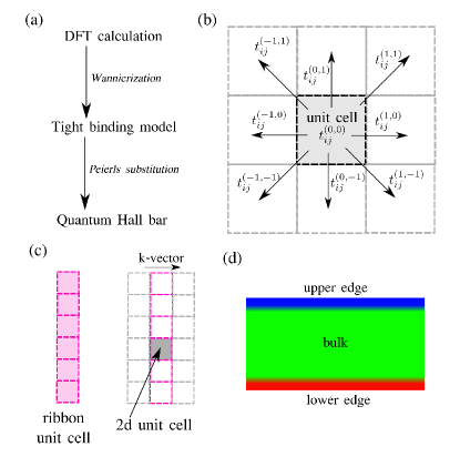
with the -th Wannier orbital in the cell . In Fig. 1b it is shown a sketch of the meaning of those matrices in real space, for the case of a square lattice and hopping to first neighboring cells.
Once we have the hopping integrals Eq. (3), obtained for the minimal unit cell that describes the 2D crystal, we can build a model for a one dimensional slab, as schematically shown in Fig. 1c. In the same step it is also possible to add the effect of the magnetic field acting on the orbital degrees of freedom using the Peierls substitution. Assuming that the bar is infinite in the direction, we use the Landau gauge that maintains the translation symmetry of the Hamiltonian, and modifies the hoppings of the 1d unit cell according to
| (4) |
where
| (5) |
is the Peierls phase, the magnetic field and the center of the different Wannier orbitals in the cells and of the 1d system. Finally, by calculating the expectation value of the position along the width of the ribbon for each state, we obtain whether a certain state is a bulk LL or an edge state (see Fig. 1d).
Since the method uses the same matrix elements for edge and bulk atoms, it completely misses the atomic scale reconstructions at the edges, such as dangling bonds and any other edge specific atomic scale process. The method assumes that the edges are identical to bulk, except for the reduced coordination. Whereas this assumption is certainly not realistic to describe atomic scale edge properties, it provides a quite reliable description of both bulk LL and even the edge states associated to propagating modes along the boundaries of the sample, whose localization length along the transverse direction is given by , much larger than the lattice constant.
III Results
III.1 Graphene
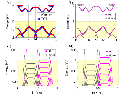
We now test the procedure with graphene.RevModPhys.81.109 In a single graphene layer, the low energy properties are dominated by two -like orbitals, one in each carbon atom. At higher energies, the decoupled bands coexist with bonding/antibonding states. To perform the Wannierization, a frozen window of eV is chosen so it contains the low energy region, whereas the outer window goes up to eV to capture the whole pz manifold. The comparison between the full DFT band structure and the Wannier band structure is shown in Fig. 2a. It is apparent that the Wannierization captures both the low energy Dirac dispersion as well as the electron hole asymmetry which arises due to second neighbor hopping.PhysRevB.88.165427
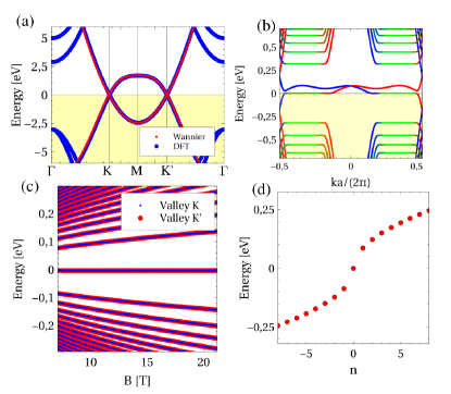
Upon application of a magnetic field in a ribbon build with the previous Hamiltonian, the familiar set of Dirac Landau levels appear. In particular (Fig. 2b), a single zero Landau level per valley shows up, that connects with zigzag edge states which show some dispersion due to the finite second neighbor hopping.PhysRevB.88.165427 Except for this feature, associated to states atomically localized at the edges, the method yields results identical to those obtained with the standard tight-binding model.katsnelson2012 The color of the bands in Fig. 2b shows the spatial location of the state: green stands for bulk111As opposed to being localized in the edge, whereas red and blue stand for top and bottom edge respectively. We can repeat the calculation for several values of and study the evolution of the Landau level spectra as a function of . We obtain the expectedzheng2002 ; katsnelson2012 square root behavior of the energy with . Independently on the magnetic field the first Landau level is always pinned at zero energy and two fold degenerate, originating one from each valley. Finally, the evolution of the LL energy for a fixed magnetic field as a function of the LL index can be obtained in the same way, showing the expected square root behavior . This further confirms the reliability of our method.
III.2 Boron nitride
Hexagonal boron nitride gorbachev2011hunting ; alem2009atomically (BN) is a two dimensional material which is mostly known for its insulating behavior and its extraordinary properties for acting as a high quality substrate for other 2D materials. young2014tunable ; PhysRevB.93.115441 ; doi:10.1021/acsnano.5b01341 ; britnell2012atomically Very much like graphene, BN consist on a honeycomb lattice, but with two inequivalent atoms, boron and nitrogen, in the unit cell. Its electronic structure is usually understood as a gapped Dirac equation in the pz manifold, having a direct band gap, although recent findings suggest that its bulk form shows an indirect gap.cassabois2015hexagonal
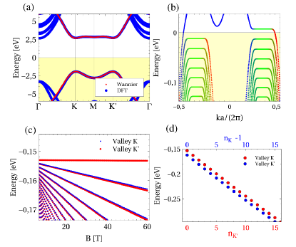
The electronic structure obtained with DFT is shown in Fig. 3a, as well as the comparison with the bands obtained via Wannierization with pz-like orbitals of boron and nitrogen. The low energy properties show a strong electron-hole asymmetry, giving rise in the conduction to a quite flat band between and , so that in the following we will focus on the more conventional valence band. In figure Fig. 3b we show the Landau levels obtained with the Wannier Hamiltonian, focusing on the valence band. It is apparent that the spectrum is different for and valleys (positive and negative values of in the figure), as expected for the case of a massive Dirac equation.koshino2010 In particular, the Landau level for holes is only present in one of the valleys. The scaling of the Landau levels with the magnetic field is shown in Fig. 3c, where it is observed the flatness with of the 0LL, expected in a massive Dirac equationkoshino2010 and the almost linear dispersion of the Landau Levels with , expected for Dirac electrons with a large mass.
III.3 MoS2
Transition metal dichalcogenides are another set of materials that can be exfoliated into 2D flakes and are attracting enormous interest.wang2012 They also have a hexagonal structure, but their electronic structure is more complicated than the one of graphene and BN, involving several orbitals of the transition metal, and also some contribution coming from the orbitals of the group VI atom.PhysRevB.88.245436 Therefore, obtaining a Slater Koster model or a tight binding model by fitting to the band structure is a very challenging task. zahid2013generic ; cappelluti2013tight ; ridolfi2015tight ; PhysRevB.88.085433 ; kormanyos2015k ; liu2015electronic Even if a good fitting is obtained, the fact that the parametrized Hamiltonian reproduces the topology and orbital character of the original Hamiltonian has to be carefully checked. In contrast, the Wannierization procedure allows to get the tight binding Hamiltonian in a single shot, reproducing both the topology and orbital weights of the bands.
Unconventional Hall effect in dichalcogenides Niu2013 ; PhysRevB.93.035406 ; PhysRevB.88.125438 is expected due to the Dirac-like nature of its band structure.xiao2012 In the following, we will focus on the case of MoS2, although a similar analysis can be applied to other transition metal dichalcogenides (TMD). We study first the conduction band, for which the effect of spin orbit coupling is much smallerPhysRevB.88.245436 than in the valence band, so that it can be initially neglected. In particular, the spin-orbit splitting in the conduction band is much smaller than the Landau level splitting for moderate values of . For the particular case of MoS2, the orbitals chosen as initial guess are the p orbitals in S and the d-orbitals in Mo, giving rise to a 11 band Hamiltonian.PhysRevB.88.245436
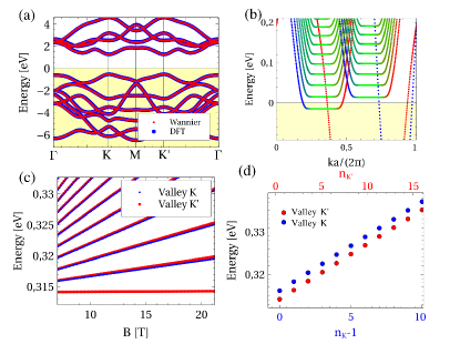
The comparison between the DFT and Wannier Hamiltonians obtained is shown in Fig. 4a. We emphasize that since the Wannierization is simply a change of basis, the orbital information is perfectly conserved between the DFT Kohn Sham states and the tight binding Hamiltonian. With the previous Hamiltonian a quantum Hall slab can be built, that permits to compute the Landau level spectra shown in Fig. 4b. Because of the lack of inversion symmetry, the Landau level in the conduction band is only present in one valley as observed in Fig. 4b. PhysRevB.90.045427 ; PhysRevLett.114.037401 In addition, for Landau indexes , a sizable valley splitting has been predicted, PhysRevB.90.045427 ; PhysRevB.91.075433 ; PhysRevB.88.125438 based on a three band tight binding model, feature that would not be observed in the Landau levels of a massive Dirac equation. Including hopping up to third neighboring cells, we find that the valley splitting in the conduction band is rather small. In comparison, if we only retain hopping to the first neighboring cell, we recover the sizable intervalley splitting predicted.PhysRevB.90.045427 ; PhysRevB.91.075433 We thus conclude that the valley splitting in the conduction band depends strongly on the details of the tight binding Hamiltonian used.
So far we have ignored the effect of spin orbit coupling. We can implement the method used so far starting from a DFT calculation that includes spin orbit coupling, and performing a Wannierization over a fully relativistic calculation. The results of this procedure are shown in Fig. 5a, and the Landau levels for the valence band in a quantum Hall slab are shown in Fig. 5c.
Nevertheless, the effect of SOC can also be captured without a fully relativistic Wannierization, but just by adding an atomic-like SOC term to the spinless Wannierization performed previously.PhysRevB.88.245436 This will be valid as long as the Wannier orbitals are atomic-like close to the atomPhysRevB.87.235109 ; PhysRevB.88.245436 (which is where the SOC has its strongest contribution), and provided the SOC splitting comes from the manifold where the Wannierization was performed. For example, in the case of graphene, the first principles SOC gap of 40 eV will be reproduced with the previous procedure only if the Wannierization includes d-orbitals of carbon,PhysRevB.80.235431 ; PhysRevB.82.245412 whereas only inclusion of sp orbitals would yield a gap 1 eV for realistic SOC coupling, PhysRevB.74.165310 ; PhysRevB.75.041401 much below the actual DFT value.
The inclusion of SOC after the Wannierization gives rise to the following Hamiltonian
| (6) |
where
| (7) |
is the atomic spin-orbit coupling. is the Wannier Hamiltonian obtained from the non relativistic DFT calculation, for the bulk or the ribbon depending on the case.
This procedure avoids having to perform a relativistic calculation, and can be useful to approximately capture SOC effects if a particular DFT code lacks of relativistic implementation, if the fully relativistic calculation is computationally too expensive, or simply to study how the band structure evolves as the SOC is turned on.PhysRevB.88.245436 It is important to note that effects produced by variations of the DFT charge density by SOC effects will not be captured, so that small differences in dispersions and effective masses are expected.
The values of and in Eq. 7 correspond approximately to the atomic SOC in Mo and S, which was shownPhysRevB.88.245436 to be on the order of 80 meV for Mo and 50 meV for S. The bulk band structure obtained with the non relativistic Wannierization plus atomic SOC following Eq.7 is shown in Fig. 5b. It is observed that this method gives a band structure in good agreement with the fully relativistic one (Fig. 5a), in particular reproducing the valley spin splitting in the and points. The quantum Hall effect in this particular system is shown in Fig. 5c for the fully relativistic Wannierization and in Fig. 5d for the non-relativistic Wannierization plus atomic SOC. In both cases it is observed that due to the large spin splitting in the valence valleys, the Landau levels are spin polarized for each valley, and with a valley-dependent spectrum for the values of the Landau index larger than . More importantly, only one of the valleys shows a single Landau level, which turns the system into a quantum spin ferromagnet upon hole doping. Although methods 5c,d give qualitative similar results, a small difference in effective mass between both calculations create a small misalignment between the levels.
Finally, it is worth to note that the previous calculations do not include nor the Zeeman term neither the coupling to the atomic orbital angular momentum , where is the atomic angular momentum, the spin, and is the Bohr magneton. This orbital coupling is internal and it is different from the orbital magnetization.PhysRevLett.95.137205 ; resta2010electrical ; PhysRevB.74.024408 In the case of MoS2, the last angular term would create a valley dependent splitting in the valence band that increases linearly with , since the states in the valence band valleys are dominated by from Mo. In comparison, its contribution in the conduction band will be much smaller, due to the dominant character. The Zeeman term would create a spin splitting in both valleys, whose effect would be more important in the conduction band, where at large enough fields would be able to compete with the small SOC splitting of the conduction band.
III.4 Black phosphorus, InSe and MoO3
In the following we will apply the method presented to other semiconducting two dimensional materials. In particular we will study cases whose low energy properties are believed to be dominated by Schrodinger-like dispersion relations, rather than Dirac like.
We first turn our attention to monolayer black phosphorus, castellanos2014isolation a two dimensional semiconductor that shows highly anisotropic electronic properties due to its distorted lattice. Its a direct gap semiconductor, with top of the valence and bottom of the conduction bands located at the point in the Brillouin zone.
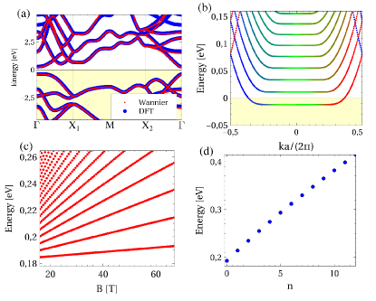
The strong mixing between s and p orbitals in black phosphorus, together with the low symmetry of the unit cells turns the fitting of its electronic structure a very challenging task if few orbitals are considered.takao1981electronic ; rudenko2014quasiparticle ; rudenko2015toward In order to properly capture the electronic structure of black phosphorus, we carry out the Wannierization with 16 Wannier orbitals , corresponding to the and orbitals of the 4 atoms of the unit cell. The inclusion of all those orbitals gives rise to a tight binding model that agrees well with the DFT eigenvalues as shown in Fig. 6a. The Wannierization with the 16 orbitals is not computationally expensive, and importantly its construction in this way warrants that all the orbital weights are properly captured.
Implementing this Hamiltonian in a one dimensional black phosphorus slab, and using the Peierls substitution, we obtain the spectrum of Landau levelszhou2015landau and edge bands shown in Fig. 6b. The anisotropic nature of the low energy properties averages out,pereira2015 ; zhou2015landau and the resulting scaling with the Landau level index (Fig. 6d) and magnetic field (Fig. 6c) are in line with those obtained using the effective mass approach.pereira2015
We now implement our method for a monolayer of indium selenide,debbichi2015two another semiconductor that can synthesized in 2D form. It shows a hexagonal lattice, very much like TMD, but with four atoms per unit cell instead of three, two In and two Se. debbichi2015two ; lauth2016solution ; lei2014evolution It has an indirect gap between the conduction band at and a Mexican hat around in valence,debbichi2015two with a direct gap of similar value. The gap is in the order of 1.6 eV, and tunable by a perpendicular electric field.debbichi2015two In addition, electroluminescenceelectroInSe as well as by confinement effectsbrotons2016nanotexturing have been recently experimentally observed.
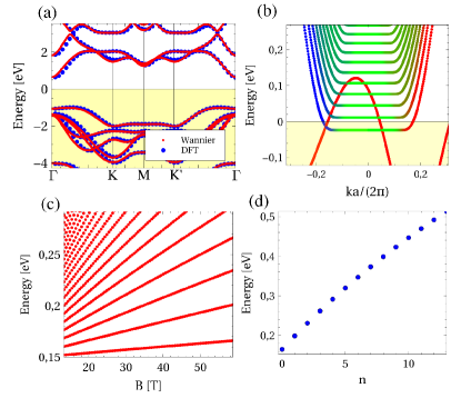
For the sake of simplicity, in the following we focus on the conduction band of InSe, that shows a minimum at . The lack of inversion symmetry will create a spin splitting in the band structure once SOC is considered, that vanishes at the point, a time reversal invariant momenta. With that in mind, we perform a non relativistic calculation, together with the Wannierization (Fig. 7a) of the InSe monolayer. The Wannierization is performed using 14 orbitals, and of In and of Se (each unit cell has 2 Se and 2 In). With the Wannier Hamiltonian, the Hall bar is created (Fig. 7b), giving rise to a conventional Landau level spectra. The scaling of the Landau level energy with the magnetic field (7c) and with the Landau index (7d) is the one of the conventional 2d electron gas. Therefore, the conduction band of InSe is one of the cleanest examples of Schrodinger dispersion in a 2d material, lacking of SOC splitting or Berry curvature effects. In striking comparison, the valence band will show both SOC effects and Berry curvature effects, since the top of the valence band is not at .
The last two dimensional material we consider is MoO3,kalantar2010synthesis another semiconducting material that can be brought to 2D formmolina2015centimeter giving rise to a bilayer system formed by two Mo planes. It has an orthorhombic unit cell, with each Mo atom sitting in an octahedral environment of O atoms. It is an indirect gap semiconductor, even in the 2D form, with a gap between the conduction band at and the valence band at .molina2015centimeter
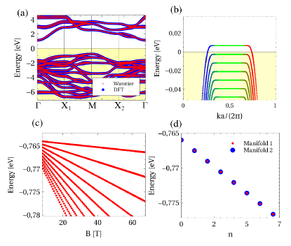
The low energy properties of this compound can be captured taking into account the d orbitals of Mo and the p orbitals of O, giving rise to tight binding Hamiltonian. In the following, we will focus on the Landau Levels of the valence band, which corresponds to the parabolic band located at . At that point, two bands coexist, which correspond to the two different Mo layers in the unit cell, each one giving rise to one set of Landau levels. The MoO3 Landau level spectrum, shown in Fig. 8b, is the one expected for Schrodinger quasiparticles, except for the twofold orbital degeneracy associated to the layer index. The degeneracy remains as we ramp the magnetic field (Fig. 8c), and for the different Landau indexes (Fig. 8d). The degeneracy could be lifted upon application of a perpendicular electric field or, more interestingly, if electronic order arises due to electron-electron interaction.
IV Landau levels as a measure of Dirac-ness
We now briefly discuss the concept of Dirac-ness and we use a recently proposed method to quantify it.goerbig2014measure There is no doubt that quasiparticles in graphene behave as Dirac electrons. However, when a given 2D crystal has a gap, things are less clear as the energy dispersion of two Schrodinger bands is very similar to the spectrum of a gapped Dirac equation. A simple way to measure the Dirac-ness of a band structure consists on looking at the evolution of the zero Landau level with magnetic field.goerbig2014measure This idea is based on the fact that for Schrodinger fermions, the energy of the Landau levels follow whereas for Dirac massive fermions in the large mass regime , where in the energy off-set of the band and m the effective mass. The previous expression can be generalized into
| (8) |
with for Dirac and for Schrodinger. Therefore, a key feature of massive Dirac fermions is that the energy of the zero Landau level is independent of the magnetic field, showing a flat evolution of the Landau level energy versus magnetic field. On the contrary, conventional Schrodinger fermions will have all their Landau levels dependent on the magnetic field, so that no flat evolution is observed.
The Dirac-ness can be easily observed by checking the Landau levels versus magnetic field as obtained for the different materials. In particular, graphene (Fig. 2c), boron nitride (Fig. 3c) and MoS2 (Fig. 4c) show a zero Landau level whose energy is independent of the magnetic field, and thereby they are Dirac materials. In contrast, black phosphorus (Fig. 6c), InSe (Fig. 7c) and MoO3 (Fig. 8c) show a first Landau level with non-zero slope. By fitting the first four Landau levels at the different magnetic fields shown in Figs. 2 3 4 6 7 8: to Eq. 8, we obtain the values shown in Table. 1.
| Material | |
|---|---|
| graphene | 0.0 |
| BN, valley (valence) | 0.024 |
| BN, valley (valence) | -0.03 |
| MoS2,valley (conduction) | 0.017 |
| MoS2, valley (conduction) | -0.03 |
| Black Phosphorus (conduction) | 0.499 |
| InSe (conduction) | 0.496 |
| MoO3 (valence) | 0.5 |
V Conclusions
We have shown that using the Wannierization procedure a faithful tight-binding representation of the DFT Hamiltonian can be obtained for several 2D materials. We have shown how the addition of a Peierls phase into the Wannier Hamiltonian permits to compute the Landau Level spectrum, both for bulk and edge states, of a variety of 2D materials, including graphene, BN, MoS2, Black Phosphorous, Indium Selenide and MoO3. The method is particularly suitable for systems lacking a reliable tight-binding model, or for which the derivation of an effective mass Hamiltonian is complicated or not available. We have also shown that by analyzing the evolution of the Landau level spectra, the Dirac-ness of the band structure can be determined, yielding a simple tool to identify materials with Dirac physics.
Acknowledgments
JFR acknowledges financial supported by MEC-Spain (FIS2013-47328-C2-2-P) and Generalitat Valenciana (ACOMP/2010/070), Prometeo. This work has been financially supported in part by FEDER funds. We thank B. Amorim and N. Garcia-Martinez for fruitful discussions. We acknowledge financial support by Marie-Curie-ITN 607904-SPINOGRAPH. J. L. Lado thanks the hospitality of the Departamento de Fisica Aplicada at the Universidad de Alicante. This work was supported by National Funds through the Portuguese Foundation for Science and Technology (FCT) in the framework of the Strategic Funding UID/FIS/04650/2013 and through project PTDC/FIS-NAN/3668/2014
Appendix A Computational details
The starting point is density functional calculations, performed with Quantum Espresso, for the unit cell of the desired 2D crystal. We use PBEPhysRevLett.77.3865 functional and the PAW pseudopotentialslejaeghere2016reproducibility for structural relaxation. Wannierization PhysRevB.56.12847 ; mostofi2008wannier90 ; PhysRevB.65.035109 ; PhysRevB.69.035108 ; RevModPhys.84.1419 is performed in kmesh, over the non relativistic calculation with PAW pseudopotentials, except for the case of relativistic MoS2 where we used norm conserving pseudopotentials. With the Wannier Hamiltonian for bulk, the tight binding Hamiltonian for the ribbon is created by taking the relevant tight binding parameters of the bulk Hamiltonian for each cell replica, considering hoppings up to third neighbouring cells.
The scaling of the Landau levels with magnetic field is calculated first by determining the position in reciprocal space of the flat Landau bands (in the case of graphene, BN and MoS2 two different regions). The diagonalization of the quantum Hall slab is performed in that kpoint, retaining only those eigenvalues whose eigenfunctions are located in the bulk to throw away edge states and dangling bond eigenvalues (see Figs. 4b, 7b). This procedure allows to study very wide ribbons, since the tight binding Hamiltonian is highly sparse and a few eigenvalues around the Fermi energy can be efficiently calculated with ARPACK.lehoucq1998arpack
References
- (1) L. Landau and E. Lifshitz, “Quantum mechanics (non-relativistic theory) course on theoretical physics, vol. 3, pergamon,” 1962.
- (2) T. Ando, A. B. Fowler, and F. Stern, “Electronic properties of two-dimensional systems,” Rev. Mod. Phys., vol. 54, pp. 437–672, Apr 1982.
- (3) K. Novoselov, A. K. Geim, S. Morozov, D. Jiang, M. Katsnelson, I. Grigorieva, S. Dubonos, and A. Firsov, “Two-dimensional gas of massless dirac fermions in graphene,” nature, vol. 438, no. 7065, pp. 197–200, 2005.
- (4) Y. Zhang, Y.-W. Tan, H. L. Stormer, and P. Kim, “Experimental observation of the quantum hall effect and berry’s phase in graphene,” Nature, vol. 438, no. 7065, pp. 201–204, 2005.
- (5) N. Gillgren, D. Wickramaratne, Y. Shi, T. Espiritu, J. Yang, J. Hu, J. Wei, X. Liu, Z. Mao, K. Watanabe, et al., “Gate tunable quantum oscillations in air-stable and high mobility few-layer phosphorene heterostructures,” 2D Materials, vol. 2, no. 1, p. 011001, 2014.
- (6) L. Li, G. J. Ye, V. Tran, R. Fei, G. Chen, H. Wang, J. Wang, K. Watanabe, T. Taniguchi, L. Yang, et al., “Quantum oscillations in a two-dimensional electron gas in black phosphorus thin films,” Nature nanotechnology, vol. 10, no. 7, pp. 608–613, 2015.
- (7) V. Tayari, N. Hemsworth, I. Fakih, A. Favron, E. Gaufrès, G. Gervais, R. Martel, and T. Szkopek, “Two-dimensional magnetotransport in a black phosphorus naked quantum well,” Nature communications, vol. 6, 2015.
- (8) L. Li, F. Yang, G. J. Ye, Z. Zhang, Z. Zhu, W. Lou, X. Zhou, L. Li, K. Watanabe, T. Taniguchi, et al., “Quantum hall effect in black phosphorus two-dimensional electron system,” Nature nanotechnology, 2016.
- (9) Z. Wu, S. Xu, H. Lu, G.-B. Liu, A. Khamoshi, T. Han, Y. Wu, J. Lin, G. Long, Y. He, et al., “Observation of valley zeeman and quantum hall effects at q valley of few-layer transition metal disulfides,” arXiv preprint arXiv:1511.00077, 2015.
- (10) B. Fallahazad, H. C. P. Movva, K. Kim, S. Larentis, T. Taniguchi, K. Watanabe, S. K. Banerjee, and E. Tutuc, “Shubnikov˘de haas oscillations of high-mobility holes in monolayer and bilayer : Landau level degeneracy, effective mass, and negative compressibility,” Phys. Rev. Lett., vol. 116, p. 086601, Feb 2016.
- (11) Y. Zheng and T. Ando, “Hall conductivity of a two-dimensional graphite system,” Physical Review B, vol. 65, no. 24, p. 245420, 2002.
- (12) X. Li, F. Zhang, and Q. Niu, “Unconventional quantum hall effect and tunable spin hall effect in dirac materials: Application to an isolated trilayer,” Phys. Rev. Lett., vol. 110, p. 066803, Feb 2013.
- (13) J. M. Pereira and M. I. Katsnelson, “Landau levels of single-layer and bilayer phosphorene,” Phys. Rev. B, vol. 92, p. 075437, Aug 2015.
- (14) S. Yuan, M. I. Katsnelson, and R. Roldán, “Quantum hall effect in biased black phosphorus,” arXiv preprint arXiv:1512.06345, 2015.
- (15) R. Saito, G. Dresselhaus, M. S. Dresselhaus, et al., Physical properties of carbon nanotubes, vol. 35. World Scientific, 1998.
- (16) M. Katsnelson, Graphene: carbon in two dimensions. Cambridge University Press, 2012.
- (17) B. I. Halperin, “Quantized hall conductance, current-carrying edge states, and the existence of extended states in a two-dimensional disordered potential,” Phys. Rev. B, vol. 25, pp. 2185–2190, Feb 1982.
- (18) L. Brey and H. A. Fertig, “Edge states and the quantized hall effect in graphene,” Phys. Rev. B, vol. 73, p. 195408, May 2006.
- (19) A. H. Castro Neto, F. Guinea, N. M. R. Peres, K. S. Novoselov, and A. K. Geim, “The electronic properties of graphene,” Rev. Mod. Phys., vol. 81, pp. 109–162, Jan 2009.
- (20) J. L. Lado, J. W. González, and J. Fernández-Rossier, “Quantum hall effect in gapped graphene heterojunctions,” Physical Review B, vol. 88, no. 3, p. 035448, 2013.
- (21) N. Marzari and D. Vanderbilt, “Maximally localized generalized wannier functions for composite energy bands,” Phys. Rev. B, vol. 56, pp. 12847–12865, Nov 1997.
- (22) A. A. Mostofi, J. R. Yates, Y.-S. Lee, I. Souza, D. Vanderbilt, and N. Marzari, “wannier90: A tool for obtaining maximally-localised wannier functions,” Computer physics communications, vol. 178, no. 9, pp. 685–699, 2008.
- (23) I. Souza, N. Marzari, and D. Vanderbilt, “Maximally localized wannier functions for entangled energy bands,” Phys. Rev. B, vol. 65, p. 035109, Dec 2001.
- (24) A. Calzolari, N. Marzari, I. Souza, and M. Buongiorno Nardelli, “Ab initio transport properties of nanostructures from maximally localized wannier functions,” Phys. Rev. B, vol. 69, p. 035108, Jan 2004.
- (25) N. Marzari, A. A. Mostofi, J. R. Yates, I. Souza, and D. Vanderbilt, “Maximally localized wannier functions: Theory and applications,” Rev. Mod. Phys., vol. 84, pp. 1419–1475, Oct 2012.
- (26) T. Thonhauser and D. Vanderbilt, “Insulator/chern-insulator transition in the haldane model,” Phys. Rev. B, vol. 74, p. 235111, Dec 2006.
- (27) K. Kośmider, J. W. González, and J. Fernández-Rossier, “Large spin splitting in the conduction band of transition metal dichalcogenide monolayers,” Phys. Rev. B, vol. 88, p. 245436, Dec 2013.
- (28) L. Chen, Z. F. Wang, and F. Liu, “Robustness of two-dimensional topological insulator states in bilayer bismuth against strain and electrical field,” Phys. Rev. B, vol. 87, p. 235420, Jun 2013.
- (29) J. Lado and V. Pardo, “Dirac topological insulator in the dz2 manifold of a honeycomb oxide,” arXiv preprint arXiv:1604.05554, 2016.
- (30) J. Jung and A. H. MacDonald, “Tight-binding model for graphene -bands from maximally localized wannier functions,” Phys. Rev. B, vol. 87, p. 195450, May 2013.
- (31) H. Huang, Z. Liu, H. Zhang, W. Duan, and D. Vanderbilt, “Emergence of a chern-insulating state from a semi-dirac dispersion,” Phys. Rev. B, vol. 92, p. 161115, Oct 2015.
- (32) E. Assmann, P. Wissgott, J. Kuneš, A. Toschi, P. Blaha, and K. Held, “woptic: optical conductivity with wannier functions and adaptive k-mesh refinement,” Computer Physics Communications, 2015.
- (33) G. Pizzi, D. Volja, B. Kozinsky, M. Fornari, and N. Marzari, “Boltzwann: A code for the evaluation of thermoelectric and electronic transport properties with a maximally-localized wannier functions basis,” Computer Physics Communications, vol. 185, no. 1, pp. 422–429, 2014.
- (34) F. Lechermann, A. Georges, A. Poteryaev, S. Biermann, M. Posternak, A. Yamasaki, and O. K. Andersen, “Dynamical mean-field theory using wannier functions: A flexible route to electronic structure calculations of strongly correlated materials,” Phys. Rev. B, vol. 74, p. 125120, Sep 2006.
- (35) A. Kretinin, G. L. Yu, R. Jalil, Y. Cao, F. Withers, A. Mishchenko, M. I. Katsnelson, K. S. Novoselov, A. K. Geim, and F. Guinea, “Quantum capacitance measurements of electron-hole asymmetry and next-nearest-neighbor hopping in graphene,” Phys. Rev. B, vol. 88, p. 165427, Oct 2013.
- (36) As opposed to being localized in the edge.
- (37) R. V. Gorbachev, I. Riaz, R. R. Nair, R. Jalil, L. Britnell, B. D. Belle, E. W. Hill, K. S. Novoselov, K. Watanabe, T. Taniguchi, et al., “Hunting for monolayer boron nitride: optical and raman signatures,” Small, vol. 7, no. 4, pp. 465–468, 2011.
- (38) N. Alem, R. Erni, C. Kisielowski, M. D. Rossell, W. Gannett, and A. Zettl, “Atomically thin hexagonal boron nitride probed by ultrahigh-resolution transmission electron microscopy,” Physical Review B, vol. 80, no. 15, p. 155425, 2009.
- (39) A. F. Young, J. Sanchez-Yamagishi, B. Hunt, S. H. Choi, K. Watanabe, T. Taniguchi, R. Ashoori, and P. Jarillo-Herrero, “Tunable symmetry breaking and helical edge transport in a graphene quantum spin hall state,” Nature, vol. 505, no. 7484, pp. 528–532, 2014.
- (40) M. Gurram, S. Omar, S. Zihlmann, P. Makk, C. Schönenberger, and B. J. van Wees, “Spin transport in fully hexagonal boron nitride encapsulated graphene,” Phys. Rev. B, vol. 93, p. 115441, Mar 2016.
- (41) G.-H. Lee, X. Cui, Y. D. Kim, G. Arefe, X. Zhang, C.-H. Lee, F. Ye, K. Watanabe, T. Taniguchi, P. Kim, and J. Hone, “Highly stable, dual-gated mos2 transistors encapsulated by hexagonal boron nitride with gate-controllable contact, resistance, and threshold voltage,” ACS Nano, vol. 9, no. 7, pp. 7019–7026, 2015. PMID: 26083310.
- (42) L. Britnell, R. V. Gorbachev, R. Jalil, B. D. Belle, F. Schedin, M. I. Katsnelson, L. Eaves, S. V. Morozov, A. S. Mayorov, N. M. Peres, et al., “Atomically thin boron nitride: a tunnelling barrier for graphene devices,” arXiv preprint arXiv:1202.0735, 2012.
- (43) G. Cassabois, P. Valvin, and B. Gil, “Hexagonal boron nitride is an indirect bandgap semiconductor,” arXiv preprint arXiv:1512.02962, 2015.
- (44) M. Koshino and T. Ando, “Anomalous orbital magnetism in dirac-electron systems: Role of pseudospin paramagnetism,” Phys. Rev. B, vol. 81, p. 195431, May 2010.
- (45) Q. H. Wang, K. Kalantar-Zadeh, A. Kis, J. N. Coleman, and M. S. Strano, “Electronics and optoelectronics of two-dimensional transition metal dichalcogenides,” Nature nanotechnology, vol. 7, no. 11, pp. 699–712, 2012.
- (46) F. Zahid, L. Liu, Y. Zhu, J. Wang, and H. Guo, “A generic tight-binding model for monolayer, bilayer and bulk mos2,” AIP Advances, vol. 3, no. 5, p. 052111, 2013.
- (47) E. Cappelluti, R. Roldán, J. Silva-Guillén, P. Ordejón, and F. Guinea, “Tight-binding model and direct-gap/indirect-gap transition in single-layer and multilayer mos 2,” Physical Review B, vol. 88, no. 7, p. 075409, 2013.
- (48) E. Ridolfi, D. Le, T. Rahman, E. Mucciolo, and C. Lewenkopf, “A tight-binding model for mos2 monolayers,” Journal of Physics: Condensed Matter, vol. 27, no. 36, p. 365501, 2015.
- (49) G.-B. Liu, W.-Y. Shan, Y. Yao, W. Yao, and D. Xiao, “Three-band tight-binding model for monolayers of group-vib transition metal dichalcogenides,” Phys. Rev. B, vol. 88, p. 085433, Aug 2013.
- (50) A. Kormányos, G. Burkard, M. Gmitra, J. Fabian, V. Zólyomi, N. D. Drummond, and V. Fal’ko, “k· p theory for two-dimensional transition metal dichalcogenide semiconductors,” 2D Materials, vol. 2, no. 2, p. 022001, 2015.
- (51) G.-B. Liu, D. Xiao, Y. Yao, X. Xu, and W. Yao, “Electronic structures and theoretical modelling of two-dimensional group-vib transition metal dichalcogenides,” Chemical Society Reviews, vol. 44, no. 9, pp. 2643–2663, 2015.
- (52) M. Tahir, P. Vasilopoulos, and F. M. Peeters, “Quantum magnetotransport properties of a monolayer,” Phys. Rev. B, vol. 93, p. 035406, Jan 2016.
- (53) F. Rose, M. O. Goerbig, and F. Piéchon, “Spin- and valley-dependent magneto-optical properties of mos2,” Phys. Rev. B, vol. 88, p. 125438, Sep 2013.
- (54) D. Xiao, G.-B. Liu, W. Feng, X. Xu, and W. Yao, “Coupled spin and valley physics in monolayers of mos 2 and other group-vi dichalcogenides,” Physical Review Letters, vol. 108, no. 19, p. 196802, 2012.
- (55) R.-L. Chu, X. Li, S. Wu, Q. Niu, W. Yao, X. Xu, and C. Zhang, “Valley-splitting and valley-dependent inter-landau-level optical transitions in monolayer quantum hall systems,” Phys. Rev. B, vol. 90, p. 045427, Jul 2014.
- (56) D. MacNeill, C. Heikes, K. F. Mak, Z. Anderson, A. Kormányos, V. Zólyomi, J. Park, and D. C. Ralph, “Breaking of valley degeneracy by magnetic field in monolayer ,” Phys. Rev. Lett., vol. 114, p. 037401, Jan 2015.
- (57) H. Rostami and R. Asgari, “Valley zeeman effect and spin-valley polarized conductance in monolayer in a perpendicular magnetic field,” Phys. Rev. B, vol. 91, p. 075433, Feb 2015.
- (58) R. Sakuma, “Symmetry-adapted wannier functions in the maximal localization procedure,” Phys. Rev. B, vol. 87, p. 235109, Jun 2013.
- (59) M. Gmitra, S. Konschuh, C. Ertler, C. Ambrosch-Draxl, and J. Fabian, “Band-structure topologies of graphene: Spin-orbit coupling effects from first principles,” Phys. Rev. B, vol. 80, p. 235431, Dec 2009.
- (60) S. Konschuh, M. Gmitra, and J. Fabian, “Tight-binding theory of the spin-orbit coupling in graphene,” Phys. Rev. B, vol. 82, p. 245412, Dec 2010.
- (61) H. Min, J. E. Hill, N. A. Sinitsyn, B. R. Sahu, L. Kleinman, and A. H. MacDonald, “Intrinsic and rashba spin-orbit interactions in graphene sheets,” Phys. Rev. B, vol. 74, p. 165310, Oct 2006.
- (62) Y. Yao, F. Ye, X.-L. Qi, S.-C. Zhang, and Z. Fang, “Spin-orbit gap of graphene: First-principles calculations,” Phys. Rev. B, vol. 75, p. 041401, Jan 2007.
- (63) T. Thonhauser, D. Ceresoli, D. Vanderbilt, and R. Resta, “Orbital magnetization in periodic insulators,” Phys. Rev. Lett., vol. 95, p. 137205, Sep 2005.
- (64) R. Resta, “Electrical polarization and orbital magnetization: the modern theories,” Journal of Physics: Condensed Matter, vol. 22, no. 12, p. 123201, 2010.
- (65) D. Ceresoli, T. Thonhauser, D. Vanderbilt, and R. Resta, “Orbital magnetization in crystalline solids: Multi-band insulators, chern insulators, and metals,” Phys. Rev. B, vol. 74, p. 024408, Jul 2006.
- (66) A. Castellanos-Gomez, L. Vicarelli, E. Prada, J. O. Island, K. Narasimha-Acharya, S. I. Blanter, D. J. Groenendijk, M. Buscema, G. A. Steele, J. Alvarez, et al., “Isolation and characterization of few-layer black phosphorus,” 2D Materials, vol. 1, no. 2, p. 025001, 2014.
- (67) Y. Takao and A. Morita, “Electronic structure of black phosphorus: tight binding approach,” Physica B+ C, vol. 105, no. 1-3, pp. 93–98, 1981.
- (68) A. N. Rudenko and M. I. Katsnelson, “Quasiparticle band structure and tight-binding model for single-and bilayer black phosphorus,” Physical Review B, vol. 89, no. 20, p. 201408, 2014.
- (69) A. Rudenko, S. Yuan, and M. Katsnelson, “Toward a realistic description of multilayer black phosphorus: From g w approximation to large-scale tight-binding simulations,” Physical Review B, vol. 92, no. 8, p. 085419, 2015.
- (70) X. Zhou, R. Zhang, J. Sun, Y. Zou, D. Zhang, W. Lou, F. Cheng, G. Zhou, F. Zhai, and K. Chang, “Landau levels and magneto-transport property of monolayer phosphorene,” Scientific reports, vol. 5, 2015.
- (71) L. Debbichi, O. Eriksson, and S. Lebègue, “Two-dimensional indium selenides compounds: An ab initio study,” The journal of physical chemistry letters, vol. 6, no. 15, pp. 3098–3103, 2015.
- (72) J. Lauth, F. E. Gorris, M. Samadi Khoshkhoo, T. Chassé, W. Friedrich, V. Lebedeva, A. Meyer, C. Klinke, A. Kornowski, M. Scheele, et al., “Solution-processed two-dimensional ultrathin inse nanosheets,” Chemistry of Materials, vol. 28, no. 6, pp. 1728–1736, 2016.
- (73) S. Lei, L. Ge, S. Najmaei, A. George, R. Kappera, J. Lou, M. Chhowalla, H. Yamaguchi, G. Gupta, R. Vajtai, et al., “Evolution of the electronic band structure and efficient photo-detection in atomic layers of inse,” ACS nano, vol. 8, no. 2, pp. 1263–1272, 2014.
- (74) N. Balakrishnan, Z. R. Kudrynskyi, M. W. Fay, G. W. Mudd, S. A. Svatek, O. Makarovsky, Z. D. Kovalyuk, L. Eaves, P. H. Beton, and A. Patanè, “Room temperature electroluminescence from mechanically formed van der waals iii–vi homojunctions and heterojunctions,” Advanced Optical Materials, vol. 2, no. 11, pp. 1064–1069, 2014.
- (75) M. Brotons-Gisbert, D. Andres-Penares, J. Suh, F. Hidalgo, R. Abargues, P. J. Rodríguez-Cantó, A. Segura, A. Cros, G. Tobias, E. Canadell, et al., “Nanotexturing to enhance photoluminescent response of atomically thin indium selenide with highly tunable band gap,” Nano Letters, 2016.
- (76) K. Kalantar-Zadeh, J. Tang, M. Wang, K. L. Wang, A. Shailos, K. Galatsis, R. Kojima, V. Strong, A. Lech, W. Wlodarski, et al., “Synthesis of nanometre-thick moo 3 sheets,” Nanoscale, vol. 2, no. 3, pp. 429–433, 2010.
- (77) A. J. Molina-Mendoza, J. L. Lado, J. Island, M. A. Niño, L. Aballe, M. Foerster, F. Y. Bruno, H. S. van der Zant, G. Rubio-Bollinger, N. Agraït, et al., “Centimeter-scale synthesis of ultrathin layered moo3 by van der waals epitaxy,” arXiv preprint arXiv:1512.04355, 2015.
- (78) M. Goerbig, G. Montambaux, et al., “Measure of diracness in two-dimensional semiconductors,” EPL (Europhysics Letters), vol. 105, no. 5, p. 57005, 2014.
- (79) J. P. Perdew, K. Burke, and M. Ernzerhof, “Generalized gradient approximation made simple,” Phys. Rev. Lett., vol. 77, pp. 3865–3868, Oct 1996.
- (80) K. Lejaeghere, G. Bihlmayer, T. Björkman, P. Blaha, S. Blügel, V. Blum, D. Caliste, I. E. Castelli, S. J. Clark, A. Dal Corso, et al., “Reproducibility in density functional theory calculations of solids,” Science, vol. 351, no. 6280, p. aad3000, 2016.
- (81) R. B. Lehoucq, D. C. Sorensen, and C. Yang, ARPACK users’ guide: solution of large-scale eigenvalue problems with implicitly restarted Arnoldi methods, vol. 6. Siam, 1998.