Suspending superconducting qubits by silicon micromachining
Abstract
We present a method for relieving aluminum 3D transmon qubits from a silicon substrate using micromachining. Our technique is a high yield, one-step deep reactive ion etch that requires no additional fabrication processes, and results in the suspension of the junction area and edges of the aluminum film. The drastic change in the device geometry affects both the dielectric and flux noise environment experienced by the qubit. In particular, the participation ratios of various dielectric interfaces are significantly modified, and suspended qubits exhibited longer ’s than non-suspended ones. We also find that suspension increases the flux noise experienced by tunable SQUID-based qubits.
The coherence times of superconducting qubits have steadily increased over the past decade due to careful engineering of the electromagnetic environment, better materials and fabrication methods, and improved device designs that minimize loss. State-of-the-art superconducting qubits with the longest lifetimes () make use of very low loss tangent dielectric substrates and have large separation between planar conductors to decrease the effect of dielectric loss in the interfaces between materials Paik et al. (2011); Barends et al. (2013); Martinis and Megrant (2014). In particular, it has been shown that for aluminum 3D transmons on sapphire, times are limited by the various interfaces between the dielectric substrate, the superconducting metal, and vacuum Wang et al. (2015). This effect can be attributed to the larger electric fields near metallic surfaces and the higher concentration of two-level systems (TLS) at disordered interfaces Martinis et al. (2005); Chang et al. (2013); Gao et al. (2008). At the same time, magnetic impurities at the surface of superconductors have been proposed as the cause of flux noise that limits the performance of SQUID based qubits and sensors Yoshihara et al. (2006); Bialczak et al. (2007); Anton et al. (2013).
In order to better understand these effects, one strategy is to drastically alter the geometry of materials and interfaces that contribute to qubit loss and decoherence. In this Letter, we present a procedure for removing the substrate and suspending aluminum Josephson junctions on silicon by micromachining. Silicon is a low-loss dielectric that offers several advantages for implementing the next generation of complex quantum circuits O‘Connell et al. (2008); Gambetta et al. (2016). Its prevalent use in the semiconductor and MEMS industries have led to a large variety of fabrication techniques that are not available for sapphire Kovacs, Maluf, and Petersen (1998). Using silicon as a substrate material enables the development of novel devices and architectures in circuit QED, such as multilayer quantum circuits that incorporate micromachined superconducting enclosures and resonators Brecht et al. (2015a, b). Substrate micromachining has also been used to reduce dielectric loss and frequency noise in niobium titanium nitride coplanar waveguide resonators on silicon Bruno et al. (2015); Barends et al. (2010). On the other hand, silicon has a more complex surface chemistry than sapphire; for example, it forms an amorphous oxide layer that may be host to a large number of TLS’s and paramagnetic impurities O‘Connell et al. (2008); Schickfus and Hunklinger (1977); Koch, DiVincenzo, and Clarke (2007).
We suspend our qubits with a simple, one-step deep reactive ion etch (DRIE) using the BOSCH process that does not require any additional steps to mask or protect the devices Laermer and Schilp (1996); Bruno et al. (2015); SUP . We begin with high resistivity (100) silicon wafers ( cm) and fabricate aluminum 3D transmon qubits using the standard Dolan bridge double-angle deposition techniqueDolan (1977). DRIE is then performed directly on the fabricated qubits. This is possible because aluminum itself is an excellent mask for the BOSCH process. We have performed this process on more than one hundred devices of various geometries, and found that the Josephson junctions were almost all unaffected except for a slight increase in the normal state resistance, possibly due to increased diffusion of the junction oxide when the devices are heated by the etching process.
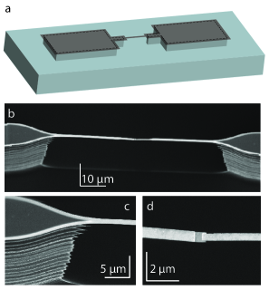
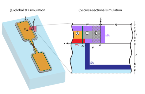
Figure 1 shows a schematic drawing and scanning electron micrographs (SEM) of suspended 3D transmons. We note that all regions 700 nm from the edge are undercut, resulting in the junction region and the narrow 1 m wide leads on either side becoming completely suspended. This means that our process is compatible with aluminum based devices of any geometry, as long as suspended metal regions are supported by other larger features. The suspended single junction transmons are robust against solvent cleaning, drying, and repeated thermal cycles. We observe, however, that more complex suspended structures such as SQUID loops are more easily damaged, for example by surface tension during solvent cleaning or wet etches.
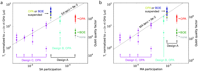
We first study the effect our process has on dielectric loss and qubit . Following the analysis in Wang et al. (2015), we quantify the loss due to various dielectric materials using their participation ratios and loss tangents (tan). In Figure 2, we plot the measured ’s of several types of qubits with different designs and fabrication procedures against the simulated participation ratios of their metal-substrate (MS) interfaces. Similar plots of versus the substrate-air (SA) and metal-air (MA) participation ratios can be found in the supplementary materials SUP . In addition to qubits of the design shown in Figure 1 (Design A), we also fabricated a set of qubit designs with higher surface participation (Designs B and C). Design C qubits have planar capacitors whose gaps can be varied to change the surface participations. Drawings of all qubit designs can be found in the supplementary materials SUP . The dielectric participation ratios were obtained through electromagnetic simulations that faithfully modeled the device geometries, including the undercut at the edge of suspended devices Wang et al. (2015); SUP .
Without any kind of surface preparation before or after aluminum deposition, the typical ’s of the Design A qubits are only a few microseconds, which is more than an order of magnitude worse than the same design on sapphire. The use of surface treatment techniques such as buffered oxide etch (BOE) or oxygen plasma ashing (OPA) SUP ; Slichter (2011) improves the lifetimes of the regular non-suspended qubits. DRIE further improves the ’s of the Design A qubits. The highest measured with this procedure was 63 s for a etch depth of 60 m, which is comparable to the ’s of typical qubits of the same design on sapphire. We note that the qubit loss is likely frequency dependent because of coupling to resonant loss channels such as TLS’s. This can lead to low ’s in exceptional cases, which we have also included in Figure 2. We will explore this further in our later discussion of flux tunable qubits.
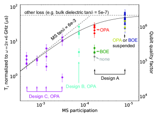
The results in Figure 2 indicate that the quality of interfaces of qubits on silicon are highly dependent on surface treatments and are generally higher loss than those on sapphire. The ’s of non-suspended Design A qubits suggest that surface treatment before and after deposition is important on silicon. On the other hand, only OPA before deposition is needed to obtain 50 s ’s on sapphire Wang et al. (2015). It is possible that, for example, the liftoff process leaves more resist residue on silicon than on sapphire. In addition, any exposed silicon surface will form an oxide even after cleaning. Both resist and oxide are likely to result in a higher loss SA interface, which has comparable participation ratios as the MS interface for non-suspended qubits. This may explain the observation that while qubit ’s are better after surface cleaning, they never reach the levels measured on sapphire.
It is also evident from Figure 2 that it is insufficient to consider a simple model where qubit loss is dominated by single dielectric interface. The qubits with high MS participation (Design C) have ’s that follow a line of constant MS tan, consistent with being limited by loss due to that interface. However, qubits with lower MS participation (Designs A and B) deviate from that line. One simple explanation for this trend is that the bulk dielectric loss for our silicon substrates becomes significant once the MS participation has been sufficiently reduced. The bulk dielectric participations of the measured qubits, including the suspended ones, are all similar to within 10. Therefore, we can indicate the limit due to bulk dielectric loss as a horizontal line in Figure 2. We find that taking into account both bulk and MS surface loss mechanisms results in a model that is consistent with data from both the suspended qubits and the regular qubits that underwent OPA.
We emphasize, however, that other loss mechanisms can play a role as well. For example, the SA and MA participations scale similarly to the MS participation for the regular, non-suspended qubitsWang et al. (2015). However, unlike a change in qubit geometry, the DRIE process affects the three interfaces differently. In particular, it increases both the SA and MA participations SUP . Therefore, increased loss from the SA and MA interfaces could contribute to negating the improvement expected from the reduced MS participation. We also cannot rule out more complex effects of the DRIE, such as a change in the SA and MA tan’s from damage or polymer deposition on these surfaces. Clearly, more investigations are needed to isolate and understand these different effects. Our results indicate that micromachining is a new technique to alter the loss contributions of various materials in ways not possible with changes in geometry alone. This can help us gain information about the roles of individual interfaces in limiting qubit ’s.
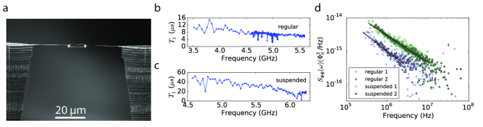
In order to investigate the effects of DRIE on qubit behavior in more detail, we also measured frequency dependence of the and flux noise of regular and suspended tunable SQUID qubits. The qubit design is exactly the same as in Figure 1, except the single junction is replaced by a 10 m 10 m SQUID loop, which is completely suspended after etching. A side-view SEM of a suspended SQUID transmon is shown in Figure 3a. We compare this device with another that underwent BOE before deposition and no other surface cleaning or etching after deposition. The two qubits were symmetrically arranged inside the same copper cavity to ensure that they experienced a similar background electromagnetic environment. Two separate solenoid coils mounted outside the cavity and aligned with the location of the qubits allowed us to individually control the frequency of each device.
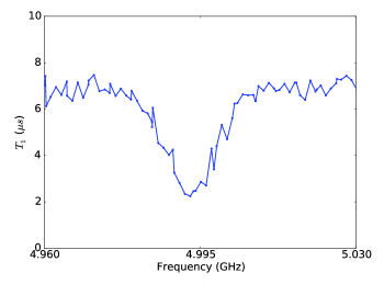
We plot as a function of qubit frequency for one pair of regular and suspended qubits in Figure 3b and 3c, respectively. For the regular qubit, we find that, in addition to a low overall of 10 s, there are sharp dips in the at a multitude of distinct frequencies. The suspended qubit shows a higher overall , but also exhibits a few resonant features where the the is drastically reduced. A second pair of qubits measured in the same manner exhibited similar behavior. These observations imply that both types of qubits are affected by the presence of resonant loss channels such as TLS’s, as was observed in many previous studies Martinis et al. (2005); Lisenfeld et al. (2015). We observe that resonant loss channels are less prevalent for the suspended qubit than the regular qubit. However, their presence may explain the variability that we observe in the measurements of single junction qubits.
The 3D SQUID transmons also allow us to investigate if and how suspension affects their magnetic environments. In particular, many previous works have observed flux noise experienced by several different types of superconducting qubits Yoshihara et al. (2006); Bialczak et al. (2007); Anton et al. (2013). It has been proposed that, similarly to dielectric loss, flux noise can be caused by defects in amorphous surface materials, such as silicon oxide Koch, DiVincenzo, and Clarke (2007). However, typical measured flux noise levels in SQUIDs have been orders of magnitude higher than estimates based on known sources, and the origin of this important dephasing mechanism for superconducting qubits remains uncertain Bylander et al. (2011); Bialczak et al. (2007); Anton et al. (2013).
In order to measure the noise power spectral density (PSD) of the qubits, we use the technique demonstrated in Bylander et al. (2011). We measure the response of the qubits to a collection of Carr-Purcell-Meiboom-Gill (CPMG) dynamical decoupling sequences with varying time delays and number of pulses to filter out noise at different frequencies. We can then use this in combination with the measured frequency-flux curves for the qubits to extract the PSD within a range of noise frequencies Bylander et al. (2011); SUP . The results are shown in Figure 3d. The PSD’s include data from two pairs of regular and suspended qubits measured in the same cavity on successive cooldowns. The data from the two pairs of qubits agree very well with each other, indicating that observed differences between the two types of qubits are not due to sample to sample variations. The flux noise for both qubits exhibits a clear power law dependence with an exponent of for the suspended qubit and for the regular qubit. We find that, while the PSD of both qubits is consistent with the range of previous measurements, the flux noise of the suspended qubits is higher than the regular qubits by a factor of of 3 in the frequency range measured. We also performed the same measurements at the zero-flux points of each qubit, and found that the PSD was essentially flat at the level of Hz. This suggests that the measured noise in this frequency range is likely to be flux-related and not due to, for example, critical current fluctuations.
While one might expect that removing the substrate from underneath the SQUID loop would decrease the flux noise due to surface spins, our data indicates that the opposite effect occurs. It has been suggested that the dominant contributors to flux inside the SQUID loop are spins on the surface of the loop traces Koch, DiVincenzo, and Clarke (2007). Therefore, removing the silicon surface inside and outside the loop may not have a large effect on the flux noise. On the other hand, DRIE also exposes the bottom surface of the aluminum loop, which forms a layer of amorphous AlOx in air. Our observations are consistent with the new AlOx layer having a higher concentration of spins than the aluminum-silicon interface, possibly because most of the SiOx was removed by BOE prior to deposition. The observation that the flux noise increased by more than a factor of two after etching could suggest that the new AlOx layer on the bottom surface contains more defects than the top surface. This might be the case given that the top oxide layer was grown in pure oxygen conditions inside the evaporator rather than through exposure to air Schneider et al. (1999). We emphasize that while this explanation is consistent with our observations, further investigation would be needed to elucidate the microscopic origins of additional flux noise in suspended qubits.
We have demonstrated that micromachining of silicon substrates is compatible with aluminum Josephson junction qubits. The process results in a reduction of the metal-substrate interface and an improvement of qubit ’s. Our results seem to suggest that we are approaching a regime where qubit decay is dominated by other mechanisms such as dielectric loss of the bulk silicon substrate. The loss tangent of “undoped” high-resistivity silicon is not very well known or understood, and is likely to be dependent on residual dopants and defects. We speculate that the DRIE technique described here, in combination with higher quality substrates, can result in qubits with even longer lifetimes. In addition, MS and bulk participation ratios can be further reduced by redesigning the qubit so that the DRIE process suspends larger areas of the device. We emphasize, however, that dielectric loss will eventually become dominated by another material. Even in the limit of a qubit floating in vacuum, there will be dielectric loss due to, for example, oxide on the surface of the metal. Beyond the reduction of dielectric loss, our measurements of flux noise with suspended SQUID transmons is another example of how qubit properties can be altered by changing the geometry of the substrate and the materials present in the environment. We expect that other potential loss mechanisms for cQED devices, such as quasiparticles and phonon couplingCatelani et al. (2011); Ioffe et al. (2004), will also be affected. Therefore, our process provides a tool for understanding and improving the various aspects involved in the performance of superconducting qubits.
We thank Luke Burkhart, Mollie Schwartz, and Michel Devoret for valuable discussions. Facilities use was supported by the Yale SEAS cleanroom, YINQE and NSF MRSEC DMR-1119826. This research was supported by the Army Research Office under Grant No. W911NF-14-1-0011. C.A. acknowledges support from the NSF Graduate Research Fellowship under Grant No. DGE-1122492. Y.Y.G. acknowledges support from an A*STAR NSS Fellowship.
Supplemental Materials for ”Suspending superconducting qubits by silicon micromachining”
I Qubit designs and fabrication procedures
Three types of 3D transmon qubit geometries were used to vary the surface participation in Figure 2 of the main text. They were similar to the designs used in Wang et al. (2015), and are shown in Figure S1. Design A, which had the lowest surface participations, was used to study the effects of DRIE etching.
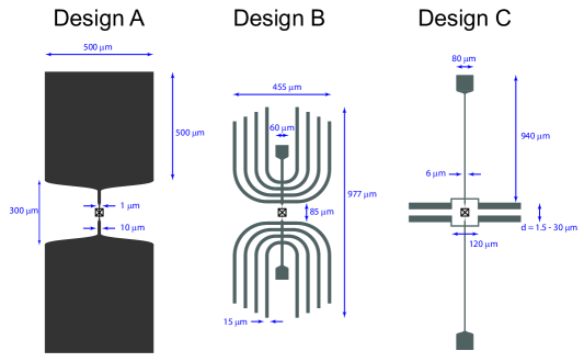
Table S1 shows the various combinations of fabrication steps performed on Design A qubits and the resulting best ’s. Fabrication of all qubits was performed using the Dolan bridge technique on 300-500 um thick (100) high resistivity ( cm) silicon wafers (Crystec and SiliconQuest). After cleaning in acetone and methanol, the wafer was spun with a bilayer of e-beam resist consisting of 500 nm of MMA (8.5) MAA EL 13 and 70 nm of 950K PMMA A3, then baked at 175 ∘C. Patterning of the qubit was done on a 100 kV VISTEC EBPG 5000+ e-beam writer, and the wafer was subsequently developed for 55 seconds in 1:3 MIBK:IPA followed by a 5 second rinse in IPA. For some of the devices, the developed wafer was then either etched in 10:1 BOE for 10 s or in an oxygen plasma asher (Glow Research AutoGlow) at 100 W for 10 s. We call this post-development step “clean 1” in Table S1. The wafer was then loaded into a Plassys e-beam evaporation system (MEB550S or UMS 300). In the case of BOE, the wafer was kept in a vacuum box during transport to the evaporator, which takes about five minutes. A bi-layer of aluminum (20 nm and 60 nm) was deposited using double-angle evaporation. In between the two layers, the junction barrier was grown by thermal oxidation using using a 85:15 Ar:O2 mixture at 15 Torr for 12 minutes. Finally, the aluminum was capped with another oxide layer grown at 3 Torr for 10 minutes. After deposition, liftoff was performed in 90 ∘C NMP for several hours, then rinsed with acetone and methanol. Prior to dicing into individual chips with one qubit each, a layer of photoresist was spun on the wafer to protect the qubits. After dicing in an ADT 7100 dicer, the resist was removed by rinsing in solvent.
The diced chips were then optionally oxygen plasma ashed (OPA) at 100 W for 3 minutes (clean 2) and/or DRIE etched. The DRIE was done using the BOSCH process with alternating SF6 inductively coupled plasma (ICP) etch (10 s, 35 mTorr, 700 W) and C4F8 ICP passivation (3s, 35 mTorr, 700 W) steps. The plasma was turned off for 1 minute after every 5 etch/passiviation cycles to prevent overheating of the sample. By changing the ratio of the etch and passivation step times, we can control the amount of undercut and the orientation of the sidewalls. A larger ratio results in a larger undercut and a sidewall that slopes more inward with etch depth. Finally, the total number cycles controls the overall depth of the etch. We find that a 10s/3s etch/passivation cycle, resulting in a 700 nm undercut, and a 60 um etch depth gives a significant modification of the participation ratios without jeopardizing the structural integrity of the devices.
After DRIE, some of the chips were processed with OPA again at 100 W for 3 minutes to remove any deposited polymer that might remain from the BOSCH process (clean 3).
| Clean 1 | Clean 2 | DRIE | Clean 3 | Max (s) |
|---|---|---|---|---|
| None | None | None | None | 4 |
| BOE | None | None | None | 6 |
| BOE | None | Yes | None | 63 |
| BOE | None | Yes | OPA | 59 |
| BOE | OPA | None | None | 7 |
| BOE | OPA | Yes | OPA | 50 |
| OPA | OPA | None | OPA | 23 |
| OPA | OPA | Yes | OPA | 44 |
II Simulations of dielectric participation
Simulations for surface and bulk dielectric participation ratios were performed a method similar to that in Wang et al. (2015). For the suspended qubits, the geometries of the various interfaces were modified accordingly, as shown in Figure S2.
The DRIE suspension processes affects the substrate-air (SA) and metal-air (MA) interfaces in a qualitatively different way than the metal-substrate (MS) interface. While it reduces the MS participation by about a factor of 5, it increases the SA participation by a factor of 4.5 and the MA participation by a factor of 3, as shown in Table S2 and S3. As mentioned in the main text, the increase of these participation ratios could contribute to additional loss in the suspended qubits, which would explain why their ’s fall below the constant MS loss tangent line in Figure 2 of the main text. However, it is evident from Figure S3 that the unetched Design A qubits have shorter ’s than would be expected from a constant MS, SA, or MA loss tangent. Therefore, as proposed in the main text, an additional loss mechanism is needed to explain this discrepancy. The simplest model assumes an effect that is independent of surface participations, such as bulk dielectric loss.
| Qubit | MS | SA | MA |
|---|---|---|---|
| Design A, suspended | 1.25e-5 | 2.90e-4 | 5.74e-6 |
| Design A, regular | 6.16e-5 | 6.40e-5 | 1.90e-6 |
| Design B, | 1.39e-4 | 1.64e-4 | 1.45e-5 |
| Design C, 30 m | 3.32e-4 | 3.83e-4 | 3.53e-5 |
| Design C, 20 m | 3.96e-4 | 4.55e-4 | 4.22e-5 |
| Design C, 10 m | 5.63e-4 | 6.49e-4 | 6.19e-5 |
| Design C, 6 m | 7.64e-4 | 8.85e-4 | 8.74e-5 |
| Design C, 3 m | 1.25e-3 | 1.46e-3 | 1.55e-4 |
| Design C, 1.5 m | 2.16e-3 | 2.36e-3 | 3.16e-4 |
III Resonant loss features
Both suspended and non-suspended flux tunable SQUID qubits exhibited dips in at certain frequencies, consistent with resonant loss mechanisms usually attributed to TLS’s in previous works Martinis et al. (2005); Lisenfeld et al. (2015). They appear to be more prevalent in the non-suspended qubits, which exhibited several of such features of various widths. A detailed measurement of versus frequency around one of these features is shown in S4.
IV Flux noise analysis
The power spectral densities (PSD) of the flux noise experienced by suspended and regular SQUID transmons were measured using dynamical decoupling techniques as described in Bylander et al. (2011). We briefly summarize the procedure here.
We applied a series of Carr-Purcell-Meiboom-Gill (CPMG) sequences Meiboom and Gill (1958), given by
| (S1) |
followed by dispersive measurement of the qubit state. The qubits were tuned to some flux point near where the was relatively long. In our case, the measured signal is given by
| (S2) |
Where is the qubit frequency, and are an overall offset and scaling determined by the qubit readout parameters, and is the PSD of the flux noise. By varying the length of the total sequence and the number of echo pulses , we can vary the center frequency and bandwidth of the filter function that makes the dynamical decoupling sequence sensitive to a particular part of the noise spectrum Álvarez and Suter (2011); Uhrig (2007). The expression for for the CPMG sequence can be found in the supplementary materials for Bylander et al. (2011).
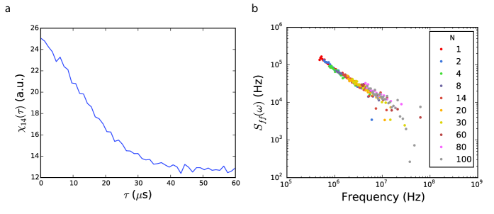
Our goal is to invert equation S2 in order to determine from the raw data. Each set of raw data consists of varying for a fix number of echo pulses, an example of which is shown in Figure S5a. We then fit the data to a functional form
| (S3) |
which takes into account the independently measured decay of the qubit and assumes a particular functional form for the dephasing, which of course depends on the flux noise PSD that we would like to determine. Therefore, the fit is only used to extract , , and , which are used to normalize the raw data and determine the range of for which the data is above the noise floor.
Next, we simplify the problem by assuming that is sharply peaked and replace it with a rectangular filter function with the same height and width. This becomes a better approximation for larger and . Using this simplified filter function, we can calculate the power spectral density of the frequency noise. An example is shown in Figure S5b after combining datasets with different ’s for one of the suspended qubits. Note that each data point in the raw data corresponds to one data point in the PSD. Finally, to convert this into flux noise, we determine by measuring the flux tuning spectrum of the qubits.
References
- Paik et al. (2011) H. Paik, D. I. Schuster, L. S. Bishop, G. Kirchmair, G. Catelani, A. P. Sears, B. R. Johnson, M. J. Reagor, L. Frunzio, L. I. Glazman, S. M. Girvin, M. H. Devoret, and R. J. Schoelkopf, Phys. Rev. Lett. 107, 240501 (2011).
- Barends et al. (2013) R. Barends, J. Kelly, A. Megrant, D. Sank, E. Jeffrey, Y. Chen, Y. Yin, B. Chiaro, J. Mutus, C. Neill, P. O’Malley, P. Roushan, J. Wenner, T. C. White, A. N. Cleland, and J. M. Martinis, Phys. Rev. Lett. 111, 080502 (2013).
- Martinis and Megrant (2014) J. M. Martinis and A. Megrant, arXiv.org (2014), 1410.5793 .
- Wang et al. (2015) C. Wang, C. Axline, Y. Y. Gao, T. Brecht, Y. Chu, L. Frunzio, M. H. Devoret, and R. J. Schoelkopf, Applied Physics Letters 107, 162601 (2015).
- Martinis et al. (2005) J. M. Martinis, K. B. Cooper, R. McDermott, M. Steffen, M. Ansmann, K. D. Osborn, K. Cicak, S. Oh, D. P. Pappas, R. W. Simmonds, and C. C. Yu, Physical Review Letters 95, 1 (2005).
- Chang et al. (2013) J. B. Chang, M. R. Vissers, A. D. Córcoles, M. Sandberg, J. Gao, D. W. Abraham, J. M. Chow, J. M. Gambetta, M. Beth Rothwell, G. A. Keefe, M. Steffen, and D. P. Pappas, Applied Physics Letters 103, 012602 (2013), http://dx.doi.org/10.1063/1.4813269.
- Gao et al. (2008) J. Gao, M. Daal, A. Vayonakis, S. Kumar, J. Zmuidzinas, B. Sadoulet, B. A. Mazin, P. K. Day, and H. G. Leduc, Applied Physics Letters 92, 152505 (2008).
- Yoshihara et al. (2006) F. Yoshihara, K. Harrabi, A. O. Niskanen, Y. Nakamura, and J. S. Tsai, Phys. Rev. Lett. 97, 167001 (2006).
- Bialczak et al. (2007) R. C. Bialczak, R. McDermott, M. Ansmann, M. Hofheinz, N. Katz, E. Lucero, M. Neeley, a. D. O’Connell, H. Wang, a. N. Cleland, and J. M. Martinis, Physical Review Letters 99, 1 (2007).
- Anton et al. (2013) S. M. Anton, J. S. Birenbaum, S. R. O’Kelley, V. Bolkhovsky, D. a. Braje, G. Fitch, M. Neeley, G. C. Hilton, H. M. Cho, K. D. Irwin, F. C. Wellstood, W. D. Oliver, A. Shnirman, and J. Clarke, Physical Review Letters 110, 2 (2013).
- O‘Connell et al. (2008) A. D. O‘Connell, M. Ansmann, R. C. Bialczak, M. Hofheinz, N. Katz, E. Lucero, C. McKenney, M. Neeley, H. Wang, E. M. Weig, A. N. Cleland, and J. M. Martinis, Applied Physics Letters 92, 112903 (2008).
- Gambetta et al. (2016) J. M. Gambetta, C. E. Murray, Y. K. K. Fung, D. T. McClure, O. Dial, W. Shanks, J. Sleight, and M. Steffen, arXiv.org (2016), 1605.08009 .
- Kovacs, Maluf, and Petersen (1998) G. T. A. Kovacs, N. I. Maluf, and K. E. Petersen, Proceedings of the IEEE 86, 1536 (1998).
- Brecht et al. (2015a) T. Brecht, W. Pfaff, C. Wang, Y. Chu, L. Frunzio, M. H. Devoret, and R. J. Schoelkopf, Npj Quantum Information 2, 16002 (2015a).
- Brecht et al. (2015b) T. Brecht, M. Reagor, Y. Chu, W. Pfaff, C. Wang, L. Frunzio, M. H. Devoret, and R. J. Schoelkopf, Applied Physics Letters 107, 192603 (2015b).
- Bruno et al. (2015) A. Bruno, G. de Lange, S. Asaad, K. L. van der Enden, N. K. Langford, and L. DiCarlo, Appl. Phys. Lett. 106, 182601 (2015).
- Barends et al. (2010) R. Barends, N. Vercruyssen, A. Endo, P. J. de Visser, T. Zijlstra, T. M. Klapwijk, and J. J. A. Baselmans, Applied Physics Letters 97, 033507 (2010).
- Schickfus and Hunklinger (1977) M. V. Schickfus and S. Hunklinger, Physics Letters A 64, 144 (1977).
- Koch, DiVincenzo, and Clarke (2007) R. H. Koch, D. P. DiVincenzo, and J. Clarke, Physical Review Letters 98, 267003 (2007).
- Laermer and Schilp (1996) F. Laermer and A. Schilp, “Method of anisotropically etching silicon,” (1996), US Patent 5501893.
- (21) See supplementary material at URL .
- Dolan (1977) G. J. Dolan, Applied Physics Letters 31 (1977).
- Slichter (2011) D. H. Slichter, Quantum Jumps and Measurement Backaction in a Superconducting Qubit, Ph.D. thesis, University of California, Berkeley (2011).
- Lisenfeld et al. (2015) J. Lisenfeld, G. J. Grabovskij, C. Müller, J. H. Cole, G. Weiss, and A. V. Ustinov, Nature Communications 6, 6182 (2015).
- Bylander et al. (2011) J. Bylander, S. Gustavsson, F. Yan, F. Yoshihara, K. Harrabi, G. Fitch, D. G. Cory, Y. Nakamura, J.-S. Tsai, and W. D. Oliver, Nature Physics 7, 21 (2011).
- Schneider et al. (1999) J. M. Schneider, A. Anders, B. Hjörvarsson, I. Petrov, K. Macák, U. Helmersson, and J.-E. Sundgren, Applied Physics Letters 74 (1999).
- Catelani et al. (2011) G. Catelani, R. J. Schoelkopf, M. H. Devoret, and L. I. Glazman, Phys. Rev. B 84, 064517 (2011).
- Ioffe et al. (2004) L. B. Ioffe, V. B. Geshkenbein, C. Helm, and G. Blatter, Phys. Rev. Lett. 93, 057001 (2004).
- Meiboom and Gill (1958) S. Meiboom and D. Gill, Review of Scientific Instruments 29 (1958).
- Álvarez and Suter (2011) G. A. Álvarez and D. Suter, Physical Review Letters 107, 1 (2011).
- Uhrig (2007) G. S. Uhrig, Phys. Rev. Lett. 98, 100504 (2007).