Germanium under high tensile stress: nonlinear dependence of direct band gap vs. strain
Abstract
Germanium is a strong candidate as a laser source for silicon photonics. It is widely accepted that the band structure of germanium can be altered by tensile strain so as to reduce the energy difference between its direct and indirect band gaps. However, the conventional gap deformation potential model most widely adopted to describe this transition happens to have been investigated only up to uniaxially loaded strains. In this work, we use a micro-bridge geometry to uniaxially stress germanium along [100] up to longitudinal strain and then perform electro-absorption spectroscopy. We accurately measure the energy gap between the conduction band at the point and the light- and heavy-hole valence bands. While the experimental results agree with the conventional linear deformation potential theory up to strain, a significantly nonlinear behavior is observed at higher strains. We measure the hydrostatic and tetragonal shear deformation potential of germanium to be and and introduce a second order deformation potential. The experimental results are found to be well described by tight-binding simulations. These new high strain coefficients will be suitable for the design of future CMOS-compatible lasers and opto-electronic devices based on highly strained germanium.
keywords:
germanium, tensile strain, electro-modulation, bandgap, tight-binding1 Introduction
Despite its indirect band gap, germanium is a promising candidate as a light emitter for the integrated silicon photonics. The application of several percent of tensile strain has been proposed to increase its optical emission efficiency. Since it reduces the energy difference between its direct and indirect band gaps, it could in principle lead to laser emission 1.
Significant efforts have been undertaken in the band gap engineering of germanium in order to overcome this energy difference. Applying high amounts of tensile strain in Ge should lead to a direct band gap behavior 2, 3. Various techniques have been proposed to reach such high strain levels, including the use of silicon nitride as an external stressor 4, 5, 6, 7, the stretching of germanium nanowires 8, 9, as well as the mechanical amplication in a micro-bridge of the small tensile strain present in a germanium layer grown on a silicon substrate 10, 11, 12.
The behavior of the direct band gap under large hydrostatic compressive stress is known to be non linear 13, 14, 15, 16. However, for the range of tensile strain which is of interest for the exploration of direct band gap germanium, in the order of several percent, the current theory is based on first order coefficients known as deformation potentials that are experimentally confirmed only up to strain for [100] uniaxial stress 17, 18, 19, 20. In particular, the most commonly cited deformation potentials predict an indirect-to-direct band gap transition at 21 leading to claims about the direct nature of the band gap based only on strain measurements 22.
In this work, we study experimentally the effects of strong uniaxial tensile stress along [100] in Ge micro-bridges using optical electro-absorption measurements. Based on the Franz-Keldysh effect, the electro-modulation techniques have proven to be more accurate than photoluminescence for the measurement of optical transitions in semiconductors such as germanium 23, 24, particularly in the transmission configuration 25. Using this technique, we demonstrate a significant nonlinearity in the strain-band gap relation.
We then compute the effects of strain on the band structure of germanium using a tight-binding model and compare this theoretical work to the spectroscopic measurements. We finally extract second-order deformation potentials from both theoretical and experimental data.
2 Electro-absorption spectroscopy
Using the method described by Suess et al.10, we fabricate highly strained germanium micro-bridges from germanium-on-insulator layers (figure 1.a to c). These structures, normally suspended in air, are brought into contact with the silicon substrate, allowing further technological steps (see method section).
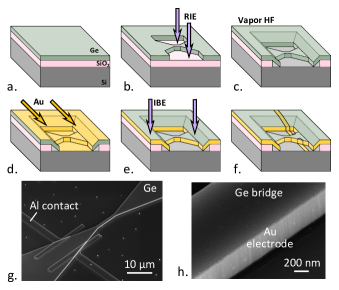
In order to perform electro-absorption spectroscopy experiments, an electric field must be applied to the strained germanium sample. For this purpose, of gold was deposited at with a planetary rotation of the sample in order to cover all the sides of the microbridges (figure 1.d). An argon Ion Beam Etching (IBE) step removed the top layer of gold, leaving about of gold only on the side walls of the patterned bridge structures (figure 1.e). Finally, deep UV lithography was employed to pattern the contacts, followed by the deposition of of aluminum. After lift-off, the gold electrodes on both sides of the micro-bridge are contacted by aluminum contacts (figure 1.f), as seen in figures 1.g and 1.h. Due to its low ultimate tensile stress ( 26) and negligible thickness, the influence of gold on the strain in germanium is estimated to be less than and can be disregarded.
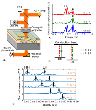
We performed electro-absorption spectroscopy for optical polarisations with an electric field parallel and perpendicular to the stress axis of the micro-bridge. Experimental electro-absorption spectra from strained micro-bridges exhibit two main oscillating components, as seen in figure 2.b. We observe an extinction of the lowest energy structure for the polarisation parallel to the bridge axis. This is explained by the selection rules for the valence bands. As shown in figure 2.c, the transition from the conduction band at the point to the heavy hole valence band has a null momentum matrix element for a light polarisation with an electric field along the stress axis, while the vertical transition with the light hole band does not exhibit such an extinction 27. It is possible to extract from this spectrum the direct band gaps to the light and heavy hole bands and . For this strained germanium microbridge (at ), we measure for instance and . Because of the low absorption coefficient of germanium at its indirect band edge, it is not possible to extract the energy of the transitions between the L valley of the conduction band and the valence bands.
By performing electro-absorption spectroscopy on micro-bridges with different stretching arm lengths, it is possible to measure the spectrum as a function of longitudinal strain, as shown in figure 2.d. For strain levels above , we clearly observe the splitting between the light and heavy hole bands. We reached strains up to and the corresponding band gaps are and .
From a set of 19 strained micro-bridge samples, we finally plotted the position of the band gaps as a function of longitudinal strain in figure 3. We first compared these experimental data points with theoretical curves obtained using deformation potentials from the model-solid theory 21 which are commonly cited for strained germanium (for instance in ref. 3, 5, 8), as plotted in figure 3. They are in very good agreement below , i.e. the deformation potentials describe well the evolution of the direct band gaps with the uniaxial [100] stress. However, experimental transition energies above are systematically lower than the theoretical curves. We therefore conclude that a first order approach using deformation potentials cannot describe precisely the behavior of the band gaps at very high strain and that higher order effects have then to be taken into account.
3 Comparison with theoretical models
We have computed the direct band gap of germanium as a function of the uniaxial [100] loading using the tight-binding model of ref. 28, adapted to the case of uniaxial stress 29. This tight-binding model was built on top of ab initio data and designed to reproduce the band structure of germanium under arbitrary strains in the range. Since this model targets the zero temperature band structure, the calculated heavy- and light-hole bandgaps were corrected for room temperature effects using Varshni’s model 30.
We plot in figure 3 the results of the simulations, as well as the experimental data points and the band gaps calculated with the deformation potentials. Experimental points are in very good agreement with the tight-binding model, which thus properly predict the evolution of the direct band gaps with strain, at least up to .
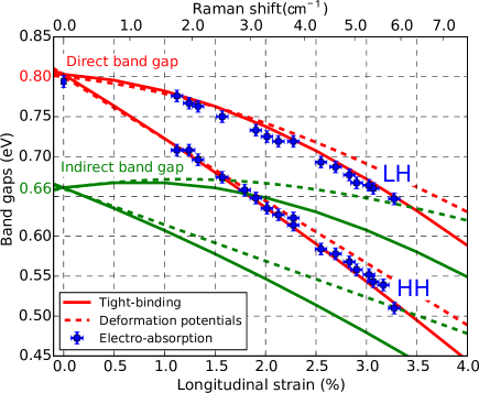
Additionally, the tight-binding model allows us to compute the evolution of the indirect band gap which cannot be observed in our experiment. We also obtain a significant nonlinearity for this transition, as seen in figure 3. This has a consequence on the position of the crossover point between the indirect and the direct band gap regimes: it is predicted to occur at , instead of for the deformation potential theory 21 as has been previously inferred in ref. 22.
To take into account the non-linearity in the relation between the band gap and strain, we introduce an extra term in the conduction band energy shifts. We choose to add a second order term because the non linearity of the tight-binding conduction band edge is an even function. Furthermore, since the usual deformation potential theory can properly describe the splitting between the light- and heavy-hole bands (both theoretically and experimentally), a second order term is not required. We also introduce a similar second order term in the expression of the indirect band gap. These second order deformation potentials, only valid for [100] uniaxial stress, allow to compute the band edges as follows:
| (1) |
| (2) |
Where (resp. ) are the direct (resp. indirect) band gaps calculated using the deformation potential theory (see supplementary information for detailed formulas).
In particular, since the heavy-hole band is fundamental for tensile uniaxial stress, we can express the relation between longitudinal strain and the lowest direct bandgap as:
| (3) |
Table 1 summarizes the deformation potentials found in this work both experimentally via the electro-absorption technique, and theoretically, via tight-binding simulations, and compares them to previous works in the literature. The linear coefficients for the conduction bands as well as the tetragonal valence band shear deformation potential from the present work exhibit very good agreement with the already published theoretical and experimental data. Fitting the tight-binding results, we of course obtain similar coefficients as published in 2009 28, but the introduction of a second order term slightly modifies the linear ones. We note however that the tight-binding deformation potential is slighly larger than experimental measurements, as it was adjusted on older data sets. In addition, the table shows the second order coefficients and we introduce to compute more precisely the evolution of the band gaps with the [100] uniaxial stress.
| Present work | Previous works | |||
|---|---|---|---|---|
| Exp. | Theor. | Exp. | Theor. | |
|
111Ref. 31
222Ref. 17 333Ref. 18 444Ref. 19 555Ref. 16 666Ref. 15 777Ref. 13 181818Ref. 39 |
888Ref. 21
999Ref. 28 101010Ref. 32 111111Ref. 33 121212Ref. 34 131313Ref. 35 141414Ref. 36 151515Ref. 37 |
|||
| – | -3.20 |
161616Ref. 38
171717Ref. 14 |
888Ref. 21
999Ref. 28 101010Ref. 32 121212Ref. 34 131313Ref. 35 141414Ref. 36 151515Ref. 37 |
|
| -2.72 |
111Ref. 31
222Ref. 17 333Ref. 18 444Ref. 19 181818Ref. 39 |
888Ref. 21
999Ref. 28 131313Ref. 35 141414Ref. 36 151515Ref. 37 |
||
| -30 | – | – | ||
| – | -35 | – | – | |
4 Conclusion
To conclude, we have measured the direct bandgap of germanium as a function of [100] uniaxial strain up to using electro-absorption spectroscopy. We demonstrate a non-linear relation between the direct band gap and the longitudinal strain. This shows that a first order theory using deformation potentials is not enough to reproduce the evolution of the band gaps of germanium at high strains. It would for instance lead to a error for the light-hole band gap at , which corresponds to an error of about in wavelength.
More precise simulations such as tight-binding modelling are required to properly describe strain-induced band gap shifts for strain levels higher than where nonlinear effects have a preeminent role.
Our experiments highlight the need for proper experimental verification of the dependence of the band structure on strain under the high strains attainable nowadays. The corrections will have a direct impact on the design of future optoelectronic and electronic devices using highly strained semiconductor layers.
This work was supported by the CEA projects ‘Phare DSM-DRT: Photonique’ and ‘Operando’ and has been performed with the help of ‘Plateforme technologique amont’ in Grenoble.
5 Methods
5.1 Strained micro-bridges fabrication
A backside polished Germanium-On-Insulator (GeOI) substrate (figure 1.a) obtained with the SmartCut™ process was used for the fabrication of the strained micro-bridges 40. These micro-bridges amplify the biaxial strain in the germanium layer resulting from the difference between the thermal expansion coefficients of silicon and germanium 10. The germanium layer was patterned with Reactive Ion Etching (RIE) using a recipe based on \ceCl2, \ceN2 and \ceO2 and of aluminium as a hard mask (figure 1.b). The resulting micro-bridges are wide, thick and long. The membranes were then released by etching the silicon dioxide sacrificial layer in a Primaxx HF vapor reactor. The release of the structure induces the retractation of the stretching arms, which put the bridge under tensile strain 10. The bridge geometry was chosen so as to obtain an homogeneous, pure tetragonal strain in the central region 41. The process used brought the whole released structure into contact with the silicon substrate, allowing further lithographic steps on the sample (figure 1.c).
5.2 Spectroscopy
Raman spectroscopy is performed to measure the strain in the micro-bridges. A laser with a output is used as a light source in a Renishaw inVia spectrometer. The resulting Raman spectrum is independent of the excitation power in this range. The Raman shift is then fitted by a Lorentzian curve and compared to the spectrum of bulk unstrained germanium. We calibrated the relationship between the Raman shift and the longitudinal uniaxial stretch along [100] using Laue X-ray micro-diffraction on selected micro-bridges (with strains up to ) at the BM32 line of the European Synchrotron Radiation Facility (ESRF) 42. X-ray diffraction indeed provides a direct measurement of the lattice parameters of the micro-bridge, thus gives a model-free measurement of strain. The obtained relationship is then fitted with a second order polynomial and used to extract strains from Raman shifts for the samples of this study. No diffraction peak broadening was observed up to the most strained bridges, indicating the absence of plasticity (at the probe location). All shear components measured by X-ray diffraction are two orders of magnitude smaller than the diagonal components.
Electro-absorption experiments were performed with a Fourier Transform Infrared (FTIR) spectrometer using a quartz-tungsten-halogen bulb as a light source and a Cassegrain objective to focus the incident light onto a single micro-bridge. The transmitted light was collected on a Thorlabs extended \ceInGaAs photodiode and the generated signal was sent to a Stanford Research Systems SR830 lock-in amplifier. The electric field was applied by a Keysight 33500B function generator outputting a positive square wave and triggering the lock-in amplifier.
References
- Liu et al. 2007 Liu, J.; Sun, X.; Pan, D.; Wang, X.; Kimerling, L. C.; Koch, T. L.; Michel, J. Tensile-strained, n-type Ge as a gain medium for monolithic laser integration on Si. Opt. Express 2007, 15, 11272–11277
- Boucaud et al. 2013 Boucaud, P.; Kurdi, M. E.; Ghrib, A.; Prost, M.; de Kersauson, M.; Sauvage, S.; Aniel, F.; Checoury, X.; Beaudoin, G.; Largeau, L.; Sagnes, I.; Ndong, G.; Chaigneau, M.; Ossikovski, R. Recent advances in germanium emission. Photon. Res. 2013, 1, 102–109
- Boztug et al. 2014 Boztug, C.; Sanchez-Perez, J. R.; Cavallo, F.; Lagally, M. G.; Paiella, R. Strained-Germanium Nanostructures for Infrared Photonics. ACS Nano 2014, 8, 3136–3151, PMID: 24597822
- de Kersauson et al. 2011 de Kersauson, M.; Kurdi, M. E.; David, S.; Checoury, X.; Fishman, G.; Sauvage, S.; Jakomin, R.; Beaudoin, G.; Sagnes, I.; Boucaud, P. Optical gain in single tensile-strained germanium photonic wire. Opt. Express 2011, 19, 17925–17934
- Jinendra et al. 2012 Jinendra, J. R.; Hryciw, A.; Baer, T. M.; Miller, D. A. B.; Brongersma, M. L.; Howe, R. T. A micromachining-based technology for enhancing germanium light emission via tensile strain. Nat Photon 2012, 6, 398–405
- Ghrib et al. 2013 Ghrib, A.; El Kurdi, M.; de Kersauson, M.; Prost, M.; Sauvage, S.; Checoury, X.; Beaudoin, G.; Sagnes, I.; Boucaud, P. Tensile-strained germanium microdisks. Applied Physics Letters 2013, 102, –
- Capellini et al. 2014 Capellini, G.; Reich, C.; Guha, S.; Yamamoto, Y.; Lisker, M.; Virgilio, M.; Ghrib, A.; Kurdi, M. E.; Boucaud, P.; Tillack, B.; Schroeder, T. Tensile Ge microstructures for lasing fabricated by means of a silicon complementary metal-oxide-semiconductor process. Opt. Express 2014, 22, 399–410
- Greil et al. 2012 Greil, J.; Lugstein, A.; Zeiner, C.; Strasser, G.; Bertagnolli, E. Tuning the Electro-optical Properties of Germanium Nanowires by Tensile Strain. Nano Letters 2012, 12, 6230–6234, PMID: 23146072
- Guilloy et al. 2015 Guilloy, K.; Pauc, N.; Gassenq, A.; Gentile, P.; Tardif, S.; Rieutord, F.; Calvo, V. Tensile Strained Germanium Nanowires Measured by Photocurrent Spectroscopy and X-ray Microdiffraction. Nano Letters 2015, 15, 2429–2433, PMID: 25759950
- Suess et al. 2013 Suess, M. J.; Geiger, R.; Minamisawa, A. R.; Schiefler, G.; Frigerio, J.; Chrastina, D.; Isella, G.; Spolenak, R.; Faist, J.; Sigg, H. Analysis of enhanced light emission from highly strained germanium microbridges. Nat Photon 2013, 7, 466–472
- Nam et al. 2013 Nam, D.; Sukhdeo, D. S.; Kang, J.-H.; Petykiewicz, J.; Lee, J. H.; Jung, W. S.; Vuckovic, J.; Brongersma, M. L.; Saraswat, K. C. Strain-Induced Pseudoheterostructure Nanowires Confining Carriers at Room Temperature with Nanoscale-Tunable Band Profiles. Nano Letters 2013, 13, 3118–3123, PMID: 23758608
- Gassenq et al. 2015 Gassenq, A. et al. 1.9 % bi-axial tensile strain in thick germanium suspended membranes fabricated in optical germanium-on-insulator substrates for laser applications. Applied Physics Letters 2015, 107, 191904
- Welber et al. 1977 Welber, B.; Cardona, M.; Tsay, Y.-F.; Bendow, B. Effect of hydrostatic pressure on the direct absorption edge of germanium. Phys. Rev. B 1977, 15, 875–879
- Ahmad and Adams 1986 Ahmad, C. N.; Adams, A. R. Electron transport and pressure coefficients associated with the and minima of germanium. Phys. Rev. B 1986, 34, 2319–2328
- Goni et al. 1989 Goni, A. R.; Syassen, K.; Cardona, M. Direct-band-gap absorption in germanium under pressure. Phys. Rev. B 1989, 39, 12921–12924
- Li et al. 1994 Li, G. H.; Goñi, A. R.; Syassen, K.; Cardona, M. Intervalley scattering potentials of Ge from direct exciton absorption under pressure. Phys. Rev. B 1994, 49, 8017–8023
- Balslev 1967 Balslev, I. Direct edge piezo-reflectance in Ge and GaAs. Solid State Communications 1967, 5, 315 – 317
- Chandrasekhar and Pollak 1977 Chandrasekhar, M.; Pollak, F. H. Effects of uniaxial stress on the electroreflectance spectrum of Ge and GaAs. Phys. Rev. B 1977, 15, 2127–2144
- Pollak and Cardona 1968 Pollak, F. H.; Cardona, M. Piezo-Electroreflectance in Ge, GaAs, and Si. Phys. Rev. 1968, 172, 816–837
- Hall 1962 Hall, J. J. Large-Strain Dependence of the Acceptor Binding Energy in Germanium. Phys. Rev. 1962, 128, 68–75
- Van de Walle 1989 Van de Walle, C. G. Band lineups and deformation potentials in the model-solid theory. Phys. Rev. B 1989, 39, 1871–1883
- Sukhdeo et al. 2014 Sukhdeo, D. S.; Nam, D.; Kang, J.-H.; Brongersma, M. L.; Saraswat, K. C. Direct bandgap germanium-on-silicon inferred from 5.7% 100 uniaxial tensile strain. Photon. Res. 2014, 2, A8–A13
- Ghosh 1968 Ghosh, A. K. Electroreflectance Spectra and Band Structure of Germanium. Phys. Rev. 1968, 165, 888–897
- Hamakawa et al. 1968 Hamakawa, Y.; Handler, P.; Germano, F. A. Interband Electro-Optical Properties of Germanium. II. Electroreflectance. Phys. Rev. 1968, 167, 709–716
- Frova et al. 1966 Frova, A.; Handler, P.; Germano, F. A.; Aspnes, D. E. Electro-Absorption Effects at the Band Edges of Silicon and Germanium. Phys. Rev. 1966, 145, 575–583
- Howatson 2012 Howatson, A. Engineering Tables and Data; Springer Netherlands, 2012
- Chuang 2012 Chuang, S. Physics of Photonic Devices; Wiley Series in Pure and Applied Optics; Wiley, 2012
- Niquet et al. 2009 Niquet, Y. M.; Rideau, D.; Tavernier, C.; Jaouen, H.; Blase, X. Onsite matrix elements of the tight-binding Hamiltonian of a strained crystal: Application to silicon, germanium, and their alloys. Phys. Rev. B 2009, 79, 245201
- Escalante et al. 2015 Escalante, J. M. et al. Non-linear model of electronic band structure to highly tensile-strained Germanium. 2015 IEEE 12th International Conference on Group IV Photonics (GFP). 2015; pp 77–78
- Varshni 1967 Varshni, Y. Temperature dependence of the energy gap in semiconductors. Physica 1967, 34, 149 – 154
- Liu et al. 2004 Liu, J.; Cannon, D. D.; Wada, K.; Ishikawa, Y.; Danielson, D. T.; Jongthammanurak, S.; Michel, J.; Kimerling, L. C. Deformation potential constants of biaxially tensile stressed epitaxial films on . Phys. Rev. B 2004, 70, 155309
- Chang et al. 1984 Chang, K.; Froyen, S.; Cohen, M. L. Pressure coefficients of band gaps in semiconductors. Solid State Communications 1984, 50, 105 – 107
- Rodriguez et al. 1986 Rodriguez, C. O.; Peltzer y Blanca, E. L.; Cappannini, O. M. First-principles determination of the sublinear dependence of the direct &) on hydrostatic pressure. Phys. Rev. B 1986, 33, 8436–8440
- Alouani et al. 1988 Alouani, M.; Brey, L.; Christensen, N. E. Calculated optical properties of semiconductors. Phys. Rev. B 1988, 37, 1167–1179
- Klenner et al. 1992 Klenner, M.; Falter, C.; Ludwig, W. Electron-phonon matrix elements and deformation potentials in silicon and germanium in the quasi-ion model. Annalen der Physik 1992, 504, 24–33
- Blacha et al. 1984 Blacha, A.; Presting, H.; Cardona, M. Deformation Potentials of k = 0 States of Tetrahedral Semiconductors. physica status solidi (b) 1984, 126, 11–36
- Schmid et al. 1990 Schmid, U.; Christensen, N.; Cardona, M. Calculated deformation potentials in Si, Ge, and GeSi. Solid State Communications 1990, 75, 39 – 43
- Balslev 1966 Balslev, I. Influence of Uniaxial Stress on the Indirect Absorption Edge in Silicon and Germanium. Phys. Rev. 1966, 143, 636–647
- El Kurdi et al. 2016 El Kurdi, M.; Prost, M.; Ghrib, A.; Sauvage, S.; Checoury, X.; Beaudoin, G.; Sagnes, I.; Picardi, G.; Ossikovski, R.; Boucaud, P. Direct band gap germanium microdisks obtained with silicon nitride stressor layers. ACS Photonics 2016,
- Reboud et al. 2015 Reboud, V.; Widiez, J.; Hartmann, J. M.; Osvaldo Dias, G.; Fowler, D.; Chelnokov, A.; Gassenq, A.; Guilloy, K.; Pauc, N.; Calvo, V.; Geiger, R.; Zabel, T.; Faist, J.; Sigg, H. Structural and optical properties of 200 mm germanium-on-insulator (GeOI) substrates for silicon photonics applications. Proc. SPIE 2015, 9367, 936714–936714–6
- Tardif et al. 2016 Tardif, S. et al. Lattice strain and tilt mapping in stressed Ge microstructures using X-ray Laue micro-diffraction and rainbow-filtering. arXiv:1603.06370 2016,
- Gassenq et al. 2016 Gassenq, A. et al. Accurate strain measurements in highly strained Ge nano-bridges. Applied Physics Letters 2016, 108, 241902