Broadband Transverse Electric Surface Wave in Silicene
Abstract
Transverse electric (TE) surface wave in silicine is theoretically investigated. The TE surface wave in silicene is found to exhibit better characteristics compared with that in graphene, in terms of a broader frequency range and more confinement to the surface which originate from the buckled structure of silicene. We found that even undoped silicene can support the TE surface wave. We expect to obtain the similar characteristics of the TE surface wave in other two-dimensional materials that have slightly buckled honeycomb lattice.
pacs:
72.20.Pa,72.10.-d,73.50.LwSurface electromagnetic waves, or simply surface waves are electromagnetic (EM) waves that propagate on the surface of a material hill2008light . Surface waves recently have attracted a lot of interest, because of their capability to transport the EM energy on the surface maier01 ; liu2006magnetic ; oulton2008hybrid ; vakil11 ; jablan09 ; hill2008light . There are two kinds of surface waves based on their polarizations; the transverse magnetic (TM) and transverse electric (TE) surface waves. In the case of TM surface wave, the component of magnetic field is transverse to the propagation direction, while the electric field has a component parallel to the propagation direction. The TM surface wave that also refers to a surface plasmon, can be seen as an electric dipole wave on the surface of material due to spatial perturbation of charge density sun2014artificial ; menabde15 . On the other hand, the TE surface wave has the component of electric field transverse to the propagation direction while the magnetic field has a component parallel to the direction of propagation. The TE surface wave can be seen as a magnetic dipole wave on the surface of material due to the self-sustained surface current oscillation sun2014artificial ; menabde15 .
It is important to note that the radiation loss of magnetic dipole is much smaller than that of electric dipole jackson1999classical . Therefore, the TE surface wave can propagate longer than TM surface wave he14 ; liu2012manipulating , which makes the TE surface wave desirable for the transporting EM energy over long distance sun2014artificial ; liu2012manipulating . However, the TE surface wave cannot exist on the surface of an conventional bulk metal because condition for generating the TE mode is limited which means that the induced surface current is not available in the conventional bulk metal maier01 ; sarid2010modern ; hill2008light ; sun2014artificial . Some efforts have been made for designing artificial materials so that the TE surface wave can be generated, such as metamaterials and a cluster of nanoparticles, which are generally complicated, hence making them less viable and accessible sun2014artificial ; ruppin2000surface ; liu2012manipulating ; liu2006magnetic .
The difficulties of generating the TE surface wave can be alleviated by using two-dimensional (2D) materials such like graphene, which is a monolayer of carbon atoms arranged in honeycomb lattice novoselov05 ; mikhailov07 . Mikhailov and Ziegler have shown that, when the imaginary part of optical conductivity of 2D material is negative (positive), the TE (TM) surface wave can propagate on the surface of the 2D materials mikhailov07 . Due to the presence of the Dirac cone in its electronic structure, the imaginary part of optical conductivity of graphene can be negative at a certain frequency range. This is in contrast to usual 2D electron gas systems, which have a positive imaginary part of optical conductivity mikhailov07 ; he14 . This unusual property has also enabled graphene to have the TE surface wave mikhailov07 ; he14 ; menabde15 ; jablan2011transverse . However, it was predicted that the TE surface wave in doped graphene may only exist for a narrow frequency range of mikhailov07 ; he14 ; menabde15 , where is the Fermi energy. Moreover, the TE surface wave in graphene is less confined in the direction perpendicular to the surface in comparison with the TM surface wave mikhailov07 ; he14 .
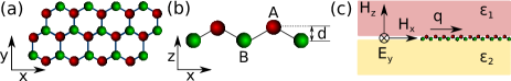
In this letter, we propose that silicene is a better 2D material rather than graphene to support the TE surface wave. Silicene is a monolayer of silicon atoms arranged in honeycomb lattice and the stable structure of silicene is not purely planar, but slightly buckled stille12 ; tabert14 ; guzman07 ; ezawa2012topological , i.e., the two sublattices are separated by vertical distance due to the -like hybridization liu2011quantum ; ezawa2012topological . The schematic structure of silicene can be seen in Figs. 1(a) and 1(b). The buckling of the atoms creates potential difference between two sublattices when an external electric field is applied in the direction perpendicular to the surface stille12 ; tabert14 ; guzman07 ; ezawa2012topological . The induced potential difference, along with the non-negligible spin orbit (SO) coupling in silicene, will give a tunable energy gap liu2011low ; stille12 ; tabert14 ; ezawa2012topological . We will show that the tunable energy gap of silicene affects a unique optical conductivity and the properties of TE surface wave which makes it a key difference from graphene.
Suppose that a silicene layer, or generally any monolayer 2D material, in the plane is sandwiched between two dielectric media with dielectric constant and as shown in Fig. 1(c). The dispersion of the TE surface wave can be obtained by employing the Maxwell equations with boundary conditions of TE wave near the surface of the layer. Here we assume that the 2D material is negligibly thin and it is characterized by its optical conductivity which will appear as a surface current density in the boundary conditions for magnetic field as shown below. The TE surface wave has an electric field in the direction and the wave vector in the direction. There are two magnetic field components and in TE surface wave as shown in Fig. 1(c). Due to the confined nature of the surface wave, the EM fields should decay in the direction perpendicular to the surface (). Thus, we can write the magnetic fields in the media and as and , respectively. The electric field in the -th medium () is obtained through . The decay constant is given by . The boundary conditions at the surface are (i) and (ii) , where is defined as surface current density. Employing the boundary conditions and assuming that the two dielectric media as vaccum (, thus ), we obtain the TE surface wave dispersion mikhailov07 ; jablan2011transverse ,
| (1) |
Since is a positive value, Eq. (1) requires a negative value of Im .
Next, we derive the of silicene. Similar to graphene, the behavior of electrons at low-energy can be described by the Dirac Hamiltonian near the K and points (hexagonal corners of Brillouin zone) stille12 ; tabert14 ; guzman07 ; ezawa2012topological . However, we should consider the following two factors: (1) the SO coupling in silicene is much larger than that of graphene liu2011low ; stille12 ; tabert14 , and (2) the potential difference between the sublattices A and B can be induced by an external perpendicular electric field stille12 ; tabert14 ; guzman07 ; ezawa2012topological . The Hamiltonian of silicene can be written in the following matrix form,
| (2) |
where is the Fermi velocity of electron and it is for silicene liu2011low . The Hamiltonian is spin and valley dependent, labeled by for spin up (spin down) and for K () valley. represents the SO coupling for silicene ezawa2012topological and denotes the potential difference between sublattices. denotes the vertical distance between the A and B atoms shown in Fig. 1(b). The eigenvalues of Eq. (2) are expressed by , with is 1 and 2 for the conduction and valence band, respectively. is the energy dispersion for electron with spin and at valley, which is given by
| (3) |
where and denotes the energy gap which is tunable by applying the up to where the structure of silicene becomes unstable drummond2012electrically . The energy gap is defined as the energy separation from the top of the valence band to the bottom of the conduction band with the same spin sign. There are only two distinct values of for four possible combination of , since and .
The optical conductivity of silicene can be obtained by the Kubo formalism for current-current correlation function falkovsky2007space ; bruus2004many . The electron scattering is ignored here. Following the derivation of graphene’s conductivity by Falkovsky and Varlamov, can be expressed by falkovsky2007space ,
| (4) |
where is the Fermi distribution function and is the matrix element of velocity matrix in the direction, where is the unitary matrix which diagonalize . The matrix is explicitly given as follows:
| (5) |
where we define , , , , , and . Here is the angle between and , while denotes the -component of the element of matrix. The first (second) term in Eq. (4) corresponds to the intraband (interband) conductivity, which is later labeled as () .
By using Eqs. (3) and (5), we can calculate in Eq. (4) for silicene at stille12 ; tabert14 . Here, is the total conductivity for both spin and valley degrees of freedom. For simplicity, we fix the meV, and vary the . Then, we get as follows
| (6) | ||||
| (7) | ||||
| (8) |
where is the Heaviside function and . If we set , we get the optical conductivity of graphene mikhailov07 ; he14 .
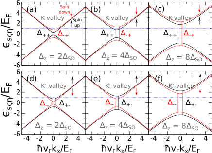
In Fig. 2, we plot the electron energy dispersions for K and K’ valleys based on Eq. (3) for several ’s. In varying , we choose three cases for both the K and K’ valleys depending on the position of relative to the energy gap, which are shown in Fig. 2. The first case is , in which is higher than bottoms of the two conduction bands for spin up and spin down ( and ) [Figs. 2(a) and 2(d)]. The second case is , in which lies between two bottoms of the conduction bands () [Figs. 2(b) and 2(e)] and the third case is , in which exists in energy gaps [Figs. 2(c) and 2(f)].
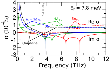
In Fig. 3, we plot the optical conductivity of silicene as a function of frequency where the solid and dashed lines are the imaginary and real parts of , respectively, for the three . We also plot the of graphene in black lines for a comparison. The logarithmic singularities in Im in Eq. (8) correspond to the lowest excitation energies for interband transitions of electrons between energy bands having the same spin directions and the same valleys. Im is singular for any frequency which satisfies condition . Since there are two distinct values of , there are two possible singularity points, and if [] or and if and []. When and there is only one singularity point at . Since of silicene depends on , of silicence can be tuned not only by but also by . As mentioned in Eq. (1), the negative value of Im correspond to the condition for TE surface wave. The TE surface wave cannot exist for the region that Im . In the following discussion, we call the frequency range of Im as the TE frequency range. Furthermore we focus only on the frequency range where Re in which the TE surface wave is not damped mikhailov07 . For graphene (), the TE frequency range is fixed at (), which reproduces the previous results mikhailov07 ; he14 .
In general, the TE frequency range in silicene is wider than that in graphene for the same and it is tunable by as shown in Fig. 3. For example, for , the TE frequency range lies within (). By increasing , increases. From Eq. (7)-(8) we know that increasing not only makes Im more negative, but also reduces Im whose value is always positive mikhailov07 . Altogether, Im decreases, hence the TE frequency range becomes wider when we increase . The Im can be suppressed when , or the Fermi level is located in [Figs. 2(b)–(c)]. This occurs for and (see Figs. 2(b) and (c) respectively). For , only Im and Im are suppressed, therefore we still have Im at certain frequency and Re for (, see Eqs. (7) and (8)). Hence, the TE frequency range becomes . But in the case of , all Im vanish and Im has negative value at all frequency. Re for (). Therefore, the TE frequency range becomes . Re appears at higher frequency than that for , because the Fermi level exists in all of the energy gaps, in which we need a higher excitation energy for interband transition.
Another interesting finding is that the undoped silicene () may also support TE surface wave. From Eqs. (6)–(8), for we get Im :
| (9) |
The TE frequency range lies within . It is noted that vanishes at in graphene mikhailov07 , hence the TE surface wave does not exist for undoped graphene.
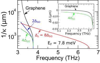
From Eq. (1), we can define a confinement length of TE surface wave , as follows
| (10) |
A smaller value of corresponds to better confinement. In Fig. 4, we plot of the TE surface wave in graphene and silicene for comparison. The plot starts at , which is the lower bound of TE frequency range in graphene. We can see that the TE surface wave in silicene is much more confined than in graphene and tunable by . For example, at , in case of graphene, , while in case of silicene, for , for , and for . In the case of , we might get a larger . This is because is singular at higher frequency, which makes for slowly diverge.
By solving Eq. (1) for , we can define the difference between the wavelength of TE surface wave and the wavelength of freely propagating EM wave in vacuum as . In the inset of Fig. 4 we plot as a function of frequency for graphene and silicene with . We can see that is sufficiently small which means that is almost the same as (3 THz corresponds to m). However, for silicene is more negative compared with that for graphene, which is almost zero. Negative means that there is shrinkage of the wavelength of TE surface wave which is the preferable feature of surface wave since more information can be compressed in the wave. From the inset of Fig. 4, we can see more shrinkage of the wavelength in silicene compared with that in graphene.
In conclusion, silicene is theoretically proved to be a versatile platform for utilizing TE surface wave. We have shown that silicene supports the TE surface wave propagation and it exhibits more preferable surface wave properties compared with those of graphene, such as the tunable broadband frequency and smaller confinement length. The TE surface wave in silicene is tunable by the Fermi energy as well as by the external electric field. These characteristics originate from the two-dimensional buckled honeycomb structure.
M.S.U. and E.H.H. are supported by the MEXT scholarship. A.R.T.N. acknowledges the Leading Graduate School Program in Tohoku University. R.S. acknowledges MEXT (Japan) Grants No. 25107005 and No. 25286005.
References
- (1) W. T. Hill III and C. H. Lee, Light-Matter Interaction (Wiley-VCH, Weinheim, 2007).
- (2) S. A. Maier, M. L. Brongersma, P. G. Kik, S. Meltzer, A. A. G. Requicha, and H. A. Atwater, Adv. Mater. 13, 1501 (2001).
- (3) H. Liu, D. A. Genov, D. M. Wu, Y. M. Liu, J. M. Steele, C. Sun, S. N. Zhu, and X. Zhang, Phys. Rev. Lett. 97, 243902 (Dec 2006).
- (4) R. F. Oulton, V. J. Sorger, D. A. Genov, D. F. P. Pile, and X. Zhang, Nature Photon. 2, 496 (2008).
- (5) A. Vakil and N. Engheta, Science 332, 1291 (2011).
- (6) M. Jablan, H. Buljan, Y. Yin, and M. Soljai, Phys. Rev. B 80, 245435 (2009).
- (7) Z. Sun, X. Zuo, T. Guan, and W. Chen, Opt. Express 22(4), 4714 (2014).
- (8) S. Menabde, D. Mason, E. Kornev, C. Lee, and N. Park, Sci. Rep. 6, 21523 (2016).
- (9) J. D. Jackson, Classical Electrodynamics (Wiley-VCH, Weinheim, 1999).
- (10) X. Y. He and R. Li, IEEE J. Sel. Top. Quantum Electron. 20, 62 (2014).
- (11) N. Liu, S. Mukherjee, K. Bao, Y. Li, L. V. Brown, P. Nordlander, and N. J. Halas, ACS Nano 6, 5482 (2012).
- (12) D. Sarid and W. Challener, Modern Introduction to Surface Plasmons: Theory, Mathematica Modeling, and Applications (Cambridge University Press, Cambridge, 2010).
- (13) R. Ruppin, Phys. Lett. A 277, 61 (2000).
- (14) K. S. Novoselov, A. K. Geim, S. V. Morozov, D. Jiang, M. I. Katsnelson, I. V. Grigorieva, S. V. Dubonos, and A. A. Firsov, Nature 438, 197 (2005).
- (15) S. A. Mikhailov and K. Ziegler, Phys. Rev. Lett. 99, 016803 (2007).
- (16) M. Jablan, H. Buljan, and M. Soljačić, Opt. Express 19, 11236 (2011).
- (17) L. Stille, C. J. Tabert, and E. J. Nicol, Phys. Rev. B 86, 195405 (2012).
- (18) C. J. Tabert and E. J. Nicol, Phys. Rev. B 89, 195410 (2014).
- (19) G. G. Guzmán-Verri and L. C. L. Y. Voon, Phys. Rev. B 76, 075131 (2007).
- (20) M. Ezawa, New J. P 14, 033003 (2012).
- (21) C.-C. Liu, W. Feng, and Y. Yao, Phys. Rev. Lett. 107, 076802 (2011).
- (22) C.-C. Liu, H. Jiang, and Y. Yao, Phys. Rev. B 84, 195430 (2011).
- (23) N. D. Drummond, V. Zolyomi, and V. I. Fal’Ko, Phys. Rev. B 85, 075423 (2012).
- (24) L. A. Falkovsky and A. A. Varlamov, EPJ B 56, 281 (2007).
- (25) H. Bruus and K. Flensberg, Many-body Quantum Theory in Condensed Matter Physics (Oxford University Press, New York, 2004).